
How Fiducial Markers Guarantee Perfect Alignment in Professional PCB Fabrication
17 min
- The Critical Role of Fiducial Markers in Modern PCB Production
- Design Guidelines for Effective Fiducial Markers
- Manufacturing Processes That Rely on Fiducial Markers
- Common Challenges and Professional Solutions
- JLCPCB's Precision in Fiducial Marker Implementation
- Frequently Asked Questions (FAQ)
Today, the most sophisticated pick-and-place machine can place a 0.5 mm pitch QFP on its footprint, board after board, thousands of times, and never miss. It is not only a matter of expensive cameras or high-quality servos, but it begins with a little, very small copper dot, simply hanging there in the corner of your PCB. That dot represents a fiducial marker, and without it, even the smoothest SMT line would be laying components in the dark.
The unrecognized heroes of automated assembly are the fiducial markers on the PCB. They provide machines with a predetermined optical reference to determine where all pad, trace, and component footprints are on the actual board. In small, high-density designs such as a CH32V003-based dev board, which is only 34.9mm by 17.9mm, full of an MCU, crystal oscillator, USB interface, indicator LEDs, and programming/GPIO headers, alignment is not an option. It is the distinction between an operational prototype and a scrap panel.
Today, I will go through all that you need to understand about fiducial markers: what they are, how to design them properly, what manufacturing processes require them, and how to circumvent the most dangerous traps. No matter whether you are deploying your first two-layer board or just scaling an established design to volume production, fiducial knowledge will make you a serious contender in the DFM game.
The Critical Role of Fiducial Markers in Modern PCB Production
What Fiducial Markers Are and Why They Matter
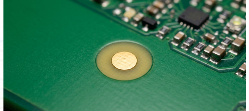
A fiducial marker is basically a small exposed copper pad (typically round) etched on the PCB surface in such a way that it can be identified by machine-vision systems. These are optical anchors of pick-and-place machines, AOI gear, and stencil printers. The system detects two or more fiducials to create a grid of coordinates that converts the real-world location and orientation of the board to the coordinate data of the design.
Fiducials may be considered the GPS satellites in a PCB assembly line. In case they are not there, the robot really does not know where the board is located on the conveyor or the fixture. It is important to distinguish between fiducials and other features that may appear similar: test pads are used to probe electrical contacts during ICT or functional tests, tooling holes are used as mechanical reference points of fixturing and panel registration when drilling. Fiducials are mere optical landmarks; on the contrary, they are not an electrical or mechanical part.
Even a tenth of a millimeter is important in the case of a board such as the CH32V003 board, whose size is less than 35 mm x 18mm. An off-stencil or a shifted pick-and-place coordinate may result in a connection between adjacent pads on the MCU or may misplace a small 0402 decoupling cap. Fiducials resolve all that uncertainty--they provide all the machines on the line with one clear reference point.
How They Enable High-Precision Automated Processes
The current SMT assembly is based on a series of processes that are aligned. Solder paste must be deposited on every pad by the stencil printer. The pick and place machine must be able to align all the components on its footprint. The AOI system is used to compare the actual solder joints with the projected design. Each of these steps corrects board offset, rotation and even a slight dimensional stretch that occurs during thermal processing using fiducial markers.
The enhancement is even quantifiable. Failure to use fiducial-based vision correction may result in a 100 to 200 micrometer drift in accuracy when placing on an average machine, simply because of variation in loading the board. When given due fiducial recognition, such an error reduces to the inherent capability of the machine, usually less than 25 microns. In fine-pitch parts such as 0.5mm pitch QFPs or 0.4mm pitch BGAs, such a difference can be the difference between clean solder joints, bridges, and openings.
In panelized builds, the fiducials are even more essential. A panel of several copies of a board, such as the CH32V003 design, requires a volume-efficiency reference in each sub-board, and also the reference fiducials of the panel frame. In the absence of this layered method, the accumulation of placement errors will occur within the panel, and it will negatively affect the yield of boards that are most distant from the initial position of the machine.
Design Guidelines for Effective Fiducial Markers
Optimal Size, Shape, and Placement Rules
Thus, the simplest fiducial design on a PCB is simply a solid circle of copper pad with a concentric solder mask opening in the center. The copper dot typically has a diameter of between 1.0 mm and 3.0 mm, among which 1.0 mm is the standard working size of SMT. The clearance of the solder mask, or the ring of open substrate that surrounds the copper, should be at least equal to the fiducial radius, and this provides the camera with an easy area to spot.
Form is important to an extent. Circular marks provide the vision system with a target that is rotationally symmetric, and centroid detection becomes much easier. It is better to avoid squares, diamonds, crosses, or anything that is not symmetrical, as this may disorient pattern recognition, provide orientation ambiguity, and increase the alignment cycle time.
Rules related to placement are also important. Avoid silkscreen text, adjacent traces, copper pours, and via pads in the fiducial area. To guarantee the camera observes a clean high-contrast target without clutter, there must be a minimum radius keep-out zone of 3 mm around the fiducial center. Position fiducials opposite the parts you are assembling. In case the board contains components on each side, simply add fiducials on each side.
| Parameter | Recommended Value | Notes |
| Copper pad diameter | 1.0 mm (typical) | Range: 1.0 - 3.0 mm per fab guidelines |
| Solder mask opening | 2.0 mm (for 1.0 mm pad) | Clearance equal to pad radius minimum |
| Keep-out zone radius | 3.0 mm minimum | No silk, traces, copper, or vias inside |
| Shape | Solid circle | No crosses, squares, or asymmetric marks |
| Surface finish | Same as board pads | HASL, ENIG, or OSP; must provide contrast |
| Minimum quantity (global) | 2 per board (3 preferred) | Diagonal or L-pattern placement |
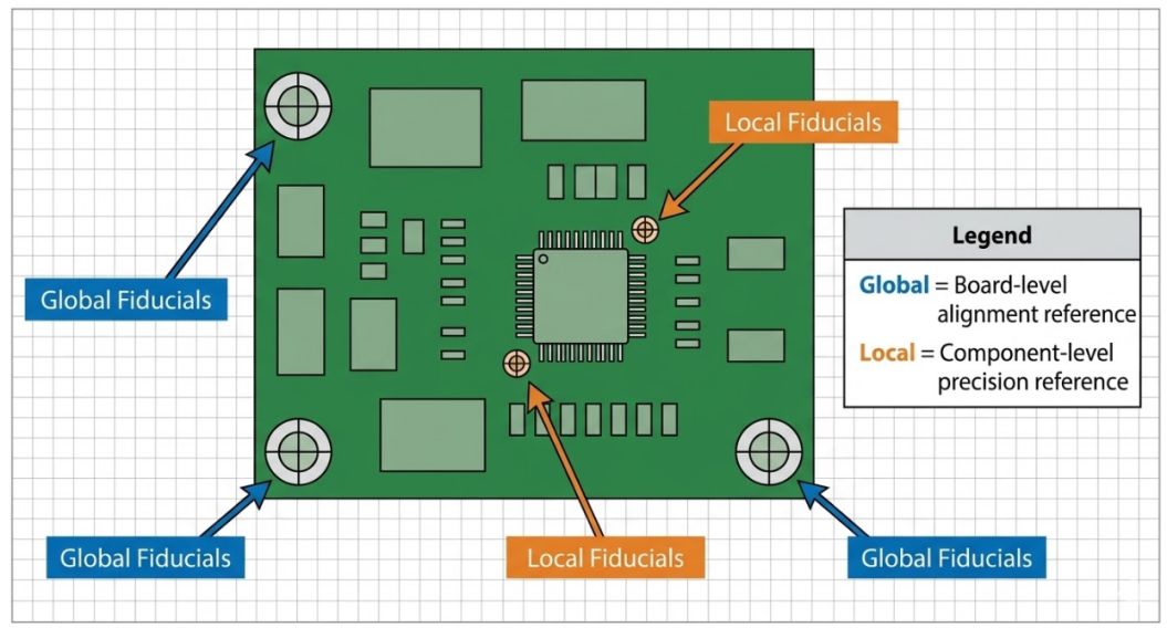
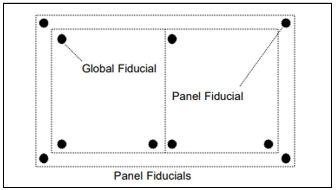
Global and Local Fiducials for Different Manufacturing Stages
In essence, there are two types of fiducials depending on the extent to which they extend. The international ones are put on the board or panel to establish the main coordinate system. At least two of them, one on each side, are required so that you may be able to determine by them where the board is and in what direction it is angled. When you add a third one in L-shape, it is even better as it will eliminate any confusion with mirror-images and will make your stretch adjustment more precise.
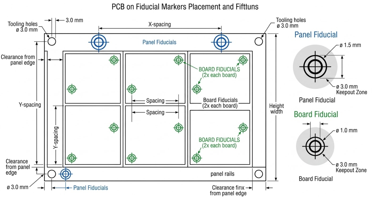
The job of local fiducials is narrower. They are placed directly adjacent to certain part footprints, typically tight fine-pitch ICs, BGAs, or QFNs, where the tolerance is the most critical. The pick-and-place machine will implement a second fine adjustment when it detects those local markers near an important component to provide the best accuracy, even when the wider global configuration has a small residual error.
The decision is quite clear in the case of the CH32V003 board. The MCU is either a TSSOP-20 or QFN-20, and has a pitch of 0.65mm or 0.5mm. Two or three of the good global fiducials normally keep things up to date on such a small board. Nevertheless, when you are using the QFN-20 that opens up a thermal pad, it is always a good idea to place a couple of local fiducials near the MCU, just in case, and particularly when you are doing mass production and looking at the highest possible first pass yield.
Manufacturing Processes That Rely on Fiducial Markers
Precise Drilling, Etching, and Solder Mask Alignment
So when your board goes even to the SMT line, fiducials are already doing the heavy lifting in the process of fabrication. To align each process layer, the PCB manufacturer relies on alignment targets, which are typically panel-level fiducials or tool features. The drilling must be accurate to fit the copper pattern, the solder mask to the pads that it is meant to reveal, and the silkscreen must superimpose the right component outlines. Should any of those registration processes become wayward, the mess simply trails the chain right to the assembly. An offset solder mask can enclose part of a pad, resulting in reduced solderable area and weak or open joints. Registration errors in drills cause the through-hole to be pushed against the annular rings, which may violate IPC-6012 Class 2 minimum requirements of a ring. Having quality fiducial targets on the manufacturing panel assists the vendor to ensure registration of layers to layers, normally 50 to 75 µm in standard procedures.
An imprecise solder mask may cover pads partially, limiting the area of wetting solder and creating weak or open joints. The registration errors of drills vary around and through-hole locations with respect to annular rings, which may result in a breach of IPC-6012 Class 2 minimum annular ring requirements. The quality fiducial targets on the fabrication panel are used to ensure that the manufacturer has the same layer-to-layer registration, usually within 50 to 75 microns in standard processes.
SMT Assembly and Automated Optical Inspection (AOI)
It is here that the fiducials literally come to the rescue. The first machine to encounter your CH32V003 board is the stencil printer when it reaches the SMT line. The vision system of the printer identifies the fiducials on the board so that the stencil apertures are positioned precisely above the pads. Off-center paste is a tombstoning recipe on small passivities or bridging on small pitch leads. Then there is the pick-and-place machine. The fiducial positions are then captured by the head-mounted camera, and then anything is placed. The software determines the offset (X, Y, and theta rotation) between the design fiducial coordinates based on the design data and the real measurements on the board.
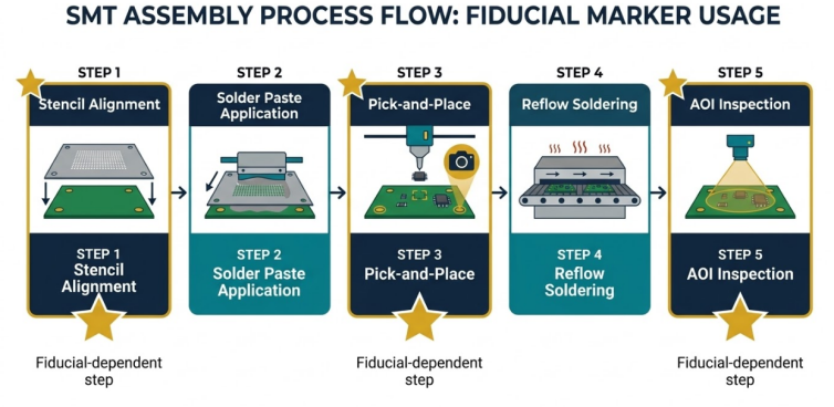
The correction is repeated on all the following component placement coordinates: the MCU, crystal, USB connector, and all 0402 passive lands are placed precisely where they should be. AOI reuses the fiducials after reflow. The inspection system requires some strong reference points to superimpose the golden image comparison on the real board. The inability of the AOI to detect fiducials reliably will lead to false defects being reported, or even worse, false defects will be overlooked. Regular fiducials make the inspection data accurate and reduce the level of defect escape.
Panelization and Depaneling Accuracy
Most production runs and even most prototype orders will panelize multiple boards at once to be efficient. An average panel to the CH32V003 board could have 20 or more copies arranged in a grid with a frame and breakaway tabs or mouse bites. It has panel rails, which are the edges of the frame surrounding the board array, which have their own fiducial markers. The fiducials used at the panel provide the assembly machine with a primary reference point in the entire array. The absence of them would force the machine to search for fiducials on every sub-board prior to component placement, which is very slow. Clean panel fiducials are used, where the machine positions the array geometry only once and steps through each board position with calculated offsets.
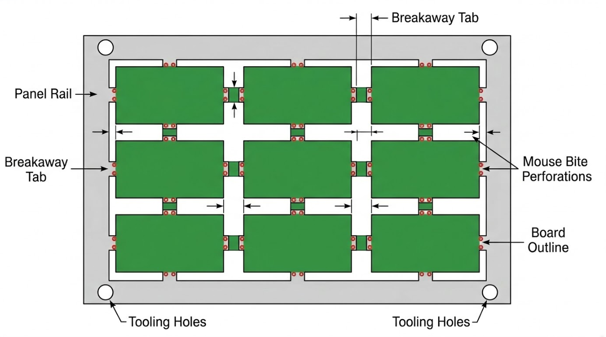
Per-board fiducial checks are also done using some machines to provide greater accuracy, particularly with large panels where thermal expansion or mechanical flex may cause outer boards to move out of the center of the panel. A sound panel fiducial policy eliminates accrued placement error. When the machine is based on panel-edge fiducials only and the panel itself is wobbling or distorting, then the boards at the far end of the array are the most erroneous. The introduction of sub-board fiducials in addition to panel fiducials produces a self-correcting system that ensures that placement accuracy remains the same throughout the entire panel, regardless of the number of boards on the panel or the size of the panel.
Common Challenges and Professional Solutions
Misalignment Risks and How to Prevent Them
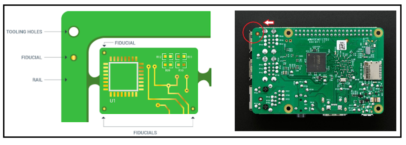
The most frequent fiducial-related failure is not that complicated: they are absent. As a student designer building SMT assembly projects, I have encountered the situation where designers unfamiliar with the SMT assembly process just ignore fiducials and learn through pad geometry that the machine will sort it out. That’s not the case. Additional common problems are fiducials that are too near the board edge, that the breakaway tabs or V-score lines are intruding into the keepout area, or fiducials obscured with silkscreen or solder mask.
Another typical problem is poor contrast. When the surrounding copper pour blends with the fiducial dot visually, the vision system will have a hard time trying to differentiate between the mark and the background. This is particularly offensive on boards of large ground pours running close to the fiducial area. The answer is to implement the solder mask clearance rules and copper keepout rules in a strict manner.
Here is a practical checklist to prevent fiducial misalignment issues:
1. Include at least two global fiducials per board, placed diagonally. Three in an L-pattern is even better.
2. Maintain a minimum 3 mm keepout radius around each fiducial, free of copper, traces, silk, and vias.
3. Verify that solder mask openings around fiducials are correctly defined in your Gerber output.
4. Place fiducials at least 5 mm from the board edge to avoid interference from panel rails or V-scores.
5. Use your EDA tool's DRC or DFM plugin to check fiducial presence and placement before submitting for fabrication.
6. For panelized designs, add three fiducials on the panel rails in addition to the per-board fiducials.
Material and Process Factors Affecting Fiducial Performance
The fiducials are highly visible, and the choice of the surface finish on your PCB is a big deal. ENIG (Electroless Nickel Immersion Gold) provides killer contrast to the solder mask since the flat, shiny gold does shine. The HASL (Hot Air Solder Leveling) is also capable of working, although the surface is not perfectly smooth and can occasionally cause the camera to give strange reflections. OSP (Organic Solderability Preservative) is far more difficult to observe, and, therefore, you have to ensure that the mask clearance is large.
| Surface Finish | Fiducial Contrast | Notes |
| ENIG | Excellent | Flat gold surface, high optical contrast against green mask |
| HASL (Lead-Free) | Good | Slightly uneven; occasional glare on reflective cameras |
| OSP | Moderate | Transparent coating on copper; needs generous mask clearance |
| Immersion Silver | Good | Bright surface; may tarnish over time if stored for long |
| Immersion Tin | Moderate to Good | Matte finish; adequate for most vision systems |
That is also painful in regard to panel stiffness and warping. When the board bends or distorts, then the fiducials are thrown out of focus, and the accuracy of the camera is lost. This is most susceptible to thin panels, particularly those of less than 1.0mm. Then, when using a thin substrate, be sure that the panel rails are broad or put in some stiffener bars or a heavier frame, so it will stay flat when it gets into the reflow oven. The lesson learned here is that you should not make your fiducials and panel design as an independent decision. A fiducial mark, the world's best will not come to the rescue of a board that warps when reflowing or a surface finish that kills the optical contrast.
JLCPCB's Precision in Fiducial Marker Implementation
Advanced Equipment for Sub-Micron Alignment Accuracy
Thus, the current SMT assembly lines, such as those of JLCPCB, are nothing but camera-directed placement, which entirely depends on fiducial marks to position boards on the assembly line. They capture those fiducial positions at sub-pixel resolution and correct offsets online in advance of each placement beat. The end result? Placement precision reaching mechanical limits of the machine, about -25 microns or better of those tiny chip-sized components.
That degree of accuracy, however, does not appear until the fiducials themselves are constructed correctly. The best machine will be as precise as the marks it measures. Poorly shaped, clogged, or missing fiducials cause the machine to come to a stop, entering it into fallback modes, hand touch-up, or simply pulling the plug on the job. This is why the fiducial implementation attached to the PCB is a precondition, and not a side-effect, of chops in the equipment.
Consistent High-Yield Production Across All Volumes
Operating on a spot such as JLCPCB provides you with a good consistency of the processes, whether ordering five boards to finalize the idea of CH32V003, or scaling up to five thousand to enter the market. Fiducial standards, panel rules, machine calibrations, etc., play the same role between prototype and full production, and therefore your first run and your thousandth run are both subject to the same alignment refs, and hit the same accuracy.
To engineers who are working around a platform, that is invaluable. You can optimize your CH32V003 board with a series of revisions - perhaps you want to include a sensor interface or replace the crystal with a MEMS oscillator - and understand that the fiducial + panel strategy that you nailed in your prototype will work directly without process drift. To get this on the board, I recommend JLCPCB combo PCB fabrication / SMT assembly service, which is just $2 for PCBs and $6 for stencil, and you can have your hardware in test within a few days.

Frequently Asked Questions (FAQ)
Q1: How many global fiducials should a small board have at a minimum?
A minimum of two global fiducials placed diagonally is required to define both position and rotation. However, three fiducials in an L-shaped pattern are strongly recommended. The third fiducial resolves mirror ambiguity and improves compensation for board stretch or dimensional variation. Even on a small board like the CH32V003 design at 34.9 mm x 17.9 mm, three fiducials are easy to fit and provide better alignment.
Q2: When are local fiducials mandatory instead of optional?
Local fiducials become mandatory when your design includes fine-pitch components with lead pitches at or below 0.5 mm, BGA packages with ball pitches at or below 0.8 mm, or QFN packages with exposed thermal pads where centering is critical for thermal and electrical performance.
Q3: Should fiducials be on the board only, panel rails only, or both?
For the best results, use both. Panel rail fiducials give the machine a fast, reliable primary reference for the entire array. Board-level fiducials provide per-unit correction that accounts for any panel distortion or dimensional variation between sub-boards.
Q4: What clearances around fiducials are usually required by assemblers?
Most assemblers require a minimum solder mask opening that is at least twice the fiducial copper diameter, creating a clear annular contrast zone. Beyond the mask opening, a keepout radius of at least 3 mm from the fiducial center should be free of any copper features, traces, silkscreen, or vias.
Keep Learning
How to Design and Manufacture Reliable Slot Holes in PCBs
Key Takeaways Slot holes are elongated openings ideal for flat pins, connectors, shields, and board alignment. Minimum sizes: 0.5 mm (plated) and 1.0 mm (non-plated); prefer rounded ends with length ≥ 2.5× width. Maintain proper annular ring, edge clearance, and DFM rules to prevent breakout and plating issues. Use overlapping drills for short plated slots and routing for longer ones. Good slot design greatly improves mechanical strength, thermal performance, and assembly reliability. JLCPCB’s precisi......
How Beveled Edges Improve Reliability and Performance in Card Edge Connectors
Key Takeaways Beveled edges enable smooth insertion and protect gold fingers from wear in card edge connectors. Use 30° or 45° angles (45° is standard for most designs) with depth of 1/3 to 1/2 board thickness. They reduce insertion force, prevent plating damage, and improve long-term contact reliability. Proper beveling is critical for high-cycle applications like DDR modules and PCIe cards. Bevel edges came into my attention the first time a memory module that I designed scratched its own gold finge......
How to Prepare Perfect Gerber Files for Flawless PCB Production
Key Takeaways Use RS-274X format and consistent millimeter units for all files. Always include complete layers: Copper, Solder Mask, Silkscreen, Board Outline, and NC Drill. Check your Gerbers in a viewer before uploading to catch errors early. Follow DFM rules: proper annular rings, solder mask expansion, and trace spacing. Use clear file naming and detailed fabrication notes. After spending weeks working on the perfect board layout, the routing is clean, the DRC passes, and you hit “export.” Two day......
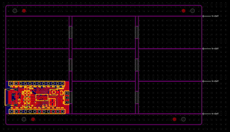
Technical Guidance: V-Cut Panelization Standards
For boards with regular rectangular shapes, V-cut (V-scoring) panelization is an efficient method. This process involves cutting V-shaped grooves of a specific depth on both sides of the panel along the board boundaries, leaving a thin web of material (typically about 1/3 of the board thickness) that allows easy manual separation after SMT assembly. After separation, minor thread-like fibers or rough edges may remain and can be lightly scraped off. Due to material expansion and cracking during depanel......
Technical Guidance: Character Design Specifications
To facilitate component assembly, future maintenance, and traceability of PCB manufacturing information (such as manufacturer, production date, batch number, etc.), various character markings are typically silk-screened onto the PCB. These include component designators, polarity marks, test point labels, company logos, and production traceability information. Traditional PCB character silk-screening uses the screen printing process, hence the term “silk-screen characters.” High-definition characters a......
Technical Guidance: Mouse Bite Panelization Guide
The conventional method of panelization uses V-grooves. However, for irregularly-shaped boards or special requirements (such as JLCPCB's economic SMT assembly), mouse bite panelization, which resembles postage stamps on an envelope, is required. PCBs panelized using this method are called "mouse bite panels" or "mouse bite connections". Mouse bite panelization can be referred to as "universal panelization." As long as there is a position to add mouse bites, boards of various shapes can be interconnect......