Solutions for High-Power Electronics: Master PCB Heat Dissipation
16 min
- Understanding Thermal Stress: Why Heat Kills Modern PCB Reliability
- Proven PCB Heat Dissipation Techniques for Thermal Efficiency
- Performing Accurate PCB Thermal Analysis and Simulation
- Advanced PCB Thermal Design and Heatsink Integration
- Manufacturing Solutions: How JLCPCB Solves Thermal Challenges
- FAQ about pcb heat dissipation
- Conclusion
- Copper Spreads Heat: Copper transfers heat over 1,000 times better than standard FR4 material.
- Thermal Via Arrays: Placing 16 to 25 vias in parallel significantly drops thermal resistance.
- MCPCB for Heavy Loads: Metal core boards offer much lower thermal resistance than FR4.
- Smart Placement: Position heat sources away from board corners and cold-sensitive components upstream.
- Calculate Junction Temp: Estimate total thermal resistance early to prevent part failure.
PCB heat dissipation is the difference between a power board that runs for ten years and one that comes back from the field in eight months. Every watt your regulator, LED, or motor driver burns has to physically leave through copper, board material, and air. If you get that path wrong, it's quiet at first. Electrolytic capacitors dry out, solder joints crack, and the board comes back as an intermittent problem that no one can duplicate on the bench. In this guide, thermal via sizing, copper and substrate selection, a complete worked example for calculating the junction temperature, heatsink integration, and a selection of thermal interface materials are described.
Understanding Thermal Stress: Why Heat Kills Modern PCB Reliability
Place a hot pan on a wooden chopping board, and the board doesn't get very warm. Place on a steel worktop, and within seconds, heat is diffused throughout the entire slab. The chopping board is Standard FR4, and the steel is your copper.
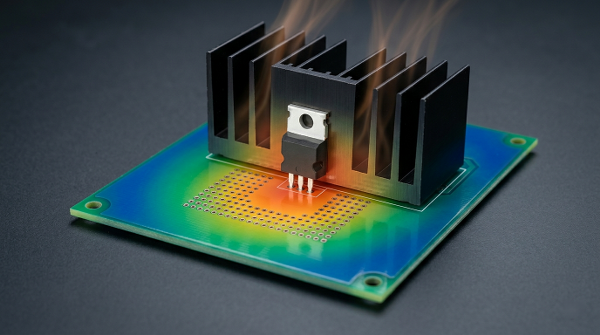
FR4 transfers 0.3 W/mK; copper transfers 400 W/mK; thus, copper is more than 1000 times better at transferring heat sideways than FR4! Heat flows like current, watts like amps, and degrees like volts, and anything in between is like a resistor.
Primary Causes of Overheating in Compact Circuits
Almost all board heat comes from four sources, and the first is usually the biggest offender.
- Linear regulators dissipate the voltage difference: An AMS1117-3.3 dropping 5 V to 3.3 V at 800 mA turns 1.36 W into heat inside a SOT-223 tab. The junction-to-ambient resistance of the tab is in the range 60 to 100 °C/W, depending on the copper to which it is attached, and increases 82 to 136 °C above the ambient air temperature.
- MOSFET and diode switching losses: These vary in proportion to frequency, and a 500 kHz converter makes much more transition loss than the same part at 100 kHz.
- Ohmic losses in the windings and copper: Heat is proportional to I squared R; thus, doubling the current quadruples the heat. A 3 A rail on a 0.5 mm (20 mil) 1 oz trace is a slow cooker.
- Core loss in inductors and ESR in electrolytics: These heat parts have no metal tab at all, so the heat has nowhere obvious to go.
The hottest portion is not necessarily the one producing the most heat. It has the poorest escape route.
The Cost of Poor Thermal Management in Industrial Applications
Heat rarely destroys a board on day one. It shortens the life of everything on it, quietly, in a way that warranty data catches long before your bench does.
You know what, every 10 °C above normal temperature reduces the life of an aluminum electrolytic capacitor by about half. A 2,000-hour, 105 °C capacitor can provide as much as 8,000 hours at 85 °C and 32,000 hours at 65 °C, which can be the difference between a three-year product life and a ten-year product life if the distance is 15 mm (0.6 in) from the hot MOSFET.
The laminate also gets damaged: Above the Tg (130 to 180 °C), the Z-axis expansion coefficient of FR4 will go from approximately 50 to 70 ppm/°C up to 250 to 350 ppm/°C, which means that the copper in your via barrels will only move at 17 ppm/°C, while the Z-axis expansion coefficient of FR4 will also be much higher. Here is our guide on how to choose the Tg of a PCB, where the higher grades have their worth. As a rule of thumb, the board should be operated 20-30 °C below its Tg.
Proven PCB Heat Dissipation Techniques for Thermal Efficiency
Only three real levers, and they work sequentially. Distribute heat side to side via copper, push it down to the other side of the board, and swap out the substrates if this is not sufficient. Start with the cheapest, because the copper you already paid for costs nothing extra.
Implementing Thermal Vias and Heavy Copper Layers
Thermal Via is a hole that is plated, which is only used to transport heat from the top copper to the bottom copper. A single 0.3 mm (12 mil) via at a 1.6 mm (63 mil) board is typically designed to be at 150 to 200 °C/W, depending on the plated thickness.
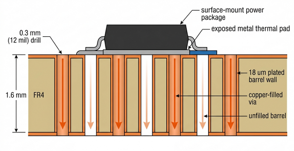
This is only useful in parallel, in which the mathematical relationship is identical to that of parallel resistors:
- Drill 0.3 mm (12 mil) holes: The larger holes pull solder from the soldering pad during the reflow process, leaving a void.
- Count them properly: Four vias provide approximately 40 °C/W, which is not measurable. Sixteen will be around 10 °C/W, and twenty-five will be around 7 °C/W.
- Fill them if the budget allows: A copper-filled via is six to eight times more thermally effective than an open barrel, and solder fill is about 70% as thermally effective, and costs less.
- Land them on true copper: Vias dissipating heat on an isolated 5 mm (0.2 in) island do virtually nothing.
The thickness of one-ounce copper is 35 µm (1.4 mil), and two ounces is 70 µm (2.8 mil). Changing to 2 oz will approximately cut in half the resistance of each heat path on the board. This is all governed by IPC-2152, which considers the thickness of a board and the thickness of the material; on outer 1 oz copper, a 1 mm (39 mil) trace can carry approximately 2.3 A per 10 °C temperature rise, and a 2 oz can carry approximately 3.9 A per 10 °C temperature rise.
Optimizing Component Placement and Airflow Routes
Placement can be done at the schematic level for free, and at the routed layout level at a cost. There are 4 rules that cover most of the benefits:
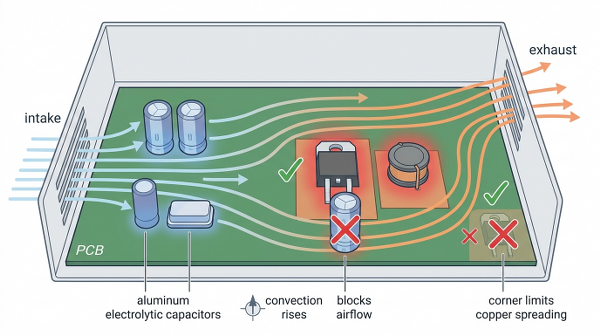
- Keep hot parts away from board corners: A corner gives copper two directions to spread into instead of four, so the same part runs measurably hotter there.
- Spread heat sources apart, unless one heatsink covers them: Two 2 W parts 5 mm (0.2 in) apart share one patch of copper and add their temperature rises together.
- Put temperature-sensitive parts upstream of the airflow: Electrolytics, crystals, and precision references belong where the air is still cool.
- Do not use a tall component in front of a hot one: A 10 mm (0.4 in) electrolytic creates a dead air pocket that can wipe out the benefit of a fan.
For natural convection, the heat transfer coefficient is approximately 5 to 10 W/m²K, and for forced air, it is 25 to 100 W/m²K. The thermal resistance of a heatsink is reduced by nearly 50% when moved at 1 m/s (around 200LFM). Our PCB Design Rules and Best Practices Guide (PDF) includes discussions about enforcing placement rules automatically.
Integrating Aluminum Substrates and Metal Core PCBs (MCPCB)
A metal core PCB replaces the fiberglass core with an aluminum or copper plate, bonded to the circuit copper by a thin insulating layer. That layer, not the metal, decides performance.
| Material | Thermal Conductivity (W/mK) | Where Is the Right Answer |
|---|---|---|
| Standard FR4 | 0.3 to 0.4 | Signal boards, anything under about 1 W per part |
| Aluminum MCPCB dielectric | 1 to 2 (up to 10 ceramic-filled) | The real bottleneck in every aluminum board |
| Aluminum base plate | 150 to 235 (about 205 typical) | LED strips, drivers, and single-layer power boards |
| Copper base plate | 380 to 400 | Automotive LEDs, loads of tens to hundreds of watts |
| Copper trace and pour | about 400 | Every board is free if you plan the pour |
Metal-core boards are fast dissipators due to the thin insulating layer, not the fast metal. That's because the dielectric is just 50-200 microns (2-8 mil) thick, and a stack with a 205 W/mK plate still works like a 1-4 W/mK stack.
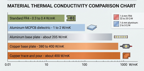
It is still an impressive achievement! A 1.6 mm (63 mil) FR4 board has a 22-25 °C/W thermal resistance, while aluminum is only 2-3 °C/W. This is why the driver in nearly every mains LED bulb is mounted on plain FR4, and it cooks itself on plain FR4 and runs cool on aluminum. The trade is that the aluminum boards are single-layer, have no plated through-holes into the core, and are generally shipped with HASL only.
Performing Accurate PCB Thermal Analysis and Simulation
There's one question analysis can answer before you spend money on a build: How hot does the silicon actually get? Hand arithmetic can provide the answer to whether the design is feasible, and simulation, plus a real board, can be used to determine whether it is correct.
Estimating Junction Temperatures and Thermal Resistance
Thermal resistance is a measure of how many degrees it will get hotter for every watt you put through it. It acts as an electrical resistor: watts are the current, the voltage drop is the degrees, and °C/W are the ohms. So if you push 2 W through 10 °C/W, you will get a 20 °C rise, as if you pushed 2 A through 10 ohms and got 20 V. The chain from silicon to air is three of those resistors in series, so you add the resistors:
Junction temperature = ambient + power × (junction-to-case + case-to-sink + sink-to-ambient)
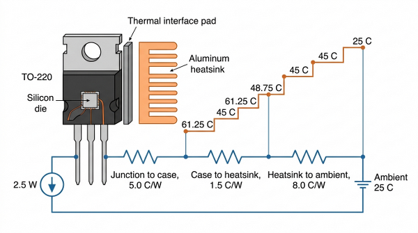
Example: An LM2596T-5.0 buck regulator in TO-220, converting 12 V to 5 V at 2 A, runs near 80% efficient and burns about 2.5 W. According to its datasheet, it has a junction-to-case thermal resistance of 2 °C/W and a maximum junction temperature of 150 °C (recommended is 125 °C).
| Step in the Heat Path | Thermal Resistance (°C/W) | Rise at 2.5 W | What It Tells You |
|---|---|---|---|
| Junction to case (datasheet) | 2.0 | 5 °C | Fixed by the package, you cannot improve it |
| Case to heatsink (silicone pad) | 1.5 | 3.75 °C | A thinner pad or grease buys a few degrees back |
| Heatsink to ambient (extruded) | 8.0 | 20 °C | The one you actually choose and pay for |
| Total with heatsink | 11.5 | 29 °C | 54 °C junction at 25 °C ambient |
The readout is that the heatsink is the dominant part of the chain; 8 of those 11.5 degrees per watt are on the heatsink, so that is where your effort should be. Within a 40 °C enclosure, the junction still only gets to 69 °C - well within the 125 °C limit.
Combining FEA Tools with Physical Prototyping
Hand math cannot solve the heat spreading that simulation tools like Ansys Icepak, SolidWorks Flow Simulation, or Cadence Celsius can. They have three errors that make their results differ from the bench.
Mistake 1: To believe the datasheet junction-to-ambient number.
It is measured on a test board specified by JEDEC and with a certain amount of copper area, which is not your board. To correct this, make use of the package property junction-to-case and compute the remainder by yourself.
Mistake 2: Bare board (no enclosure).
An open board in still air is the simplest thermal environment to be found, and virtually no product ships like that. To correct this: Model the enclosure walls and use ambient as the internal air temperature.
Mistake 3: Import copper percentage fill.
Smearing "60% copper" over a layer obscures the actual gaps and splits that are heat barriers. To correct this: Import the true copper polygons from your Gerber data.
Do not rely on an IR camera looking at bare copper. Shiny copper has an emissivity close to 0.03, and reads much cooler than it should, while green solder mask is close to 0.9 and reads as expected. Place a drop of matte black paint on any metal surface to be measured.
Advanced PCB Thermal Design and Heatsink Integration
If copper and substrate are performing to their best ability, the rest of the heat must pass through a metal object to the air. A heatsink is actually a piece of more surface area than your board has. Two factors determine if it works: fin geometry and the part-to-metal interface.
Key Guidelines for Custom PCB Heatsink Design
When stating or designing one, follow this order.
- Determine your cooling-mode fin spacing: Natural convection requires 6 to 12 mm (0.24 to 0.47 in) between the fins to allow warm air to rise out. Forced air can fall to 2 to 4 mm (0.08 to 0.16 in) as a fan will blow air through.
- Allow the base to thicken up so that it can be spread: The 3 to 5 mm (0.12 to 0.20 in) base allows heat from a 10 mm (0.4 in) package to pass to the outside of the fins rather than stacking under the part.
- Natural convection only: Use anodized black. The contribution from radiation from a black surface in still air is about 10% to 15%, and not much if a fan is in operation.
Manufacturing Solutions: How JLCPCB Solves Thermal Challenges
All the above decisions are a manufacturing specification as soon as you place the order. A thing that a fab does or doesn't offer is copper weight (fill) and substrate.
High-Thermal-Conductivity Materials and Heavy Copper Stackups
If you don't match your material to the watts, you're not routing anything.
- Heavy copper on FR4: Board thickness is determined by the weight of the outer layers (1, 2, 2.5, 3.5, or 4.5 oz) and the weight of the inner layers (0.5, 1, or 2 oz). Moving from 1 oz to 2 oz approximately halves the spreading resistance for each pour.
- Aluminum core: The typical 1 W/mK dielectric is 3-4 times better than FR4 through the thickness, and it is appropriate for LED boards, drivers, and single-layer power stages.
- Directly connected to the heatsink and copper core: The core can be exposed as a contact area of 1 × 1 mm (39 × 39 mil) or greater, and a heatsink makes contact with metal as opposed to laminate.
Compare substrates and request a quote instantly at JLCPCB's quoting page, such as aluminum-core and copper-core substrates, as well as the typical FR4.
Precision Thermal Via Plating and Advanced Aluminum PCB Production
The real success or failure of thermal designs is in via plating, where there is no indication that heat is being utilized by the board other than the copper in the barrel.
- Average hole plating thickness of 18 µm (0.7 mil): Do not use an optimistic 25 µm (1 mil) per-via thermal resistance.
- Vias as small as 0.15 mm (6 mil) can be used, but 0.3 mm (12 mil) remains the preferred size for thermal arrays because it conducts about twice as well per hole.
- Via in pad, epoxy or copper paste filled and capped: If the array under an exposed pad is doing thermal work, select copper paste, as it conducts, and epoxy does not.
When adding parts to the board in addition to fabricating it, power parts are drawn directly from the component library, and the regulator and its footprint remain the same from schematic to assembly.
FAQ about pcb heat dissipation
Q: What is the fastest way to improve heat dissipation on an existing PCB design?
Enlarge the copper pour connected to the hot component and add thermal vias underneath it. Both are free at the layout stage and can drop a component temperature by 20 to 40 °C without touching the schematic or the bill of materials.
Q:How many thermal vias do I need under a power component?
Aim for a full grid across the thermal pad at 1.0 to 1.2 mm (39 to 47 mil) spacing, which usually means 16 to 25 vias. A single 0.3 mm (12 mil) via is roughly 150 to 200 °C/W, so only a large parallel group produces a meaningful drop.
Q: Is an aluminum PCB always better than FR4 for heat dissipation?
For heat, yes, since a 1.6 mm (63 mil) aluminum board sits near 2 to 3 °C/W through its thickness against 22 to 25 °C/W for FR4. It is not always the right choice, because aluminum boards are single-layer, cannot use plated through holes into the core, and cost more.
Q: Does adding a heatsink to a small surface-mount part on FR4 actually help?
Only if the heat can reach it. A heatsink glued to a plastic package fights the package's own poor conduction, so the gain is usually a few degrees. Heat leaving through the exposed pad into the copper and vias is almost always the larger path.
Q: Does a thicker PCB dissipate heat better?
Not through its thickness, since more FR4 between the top and bottom copper means more thermal resistance. A thicker board helps only when the extra layers carry more internal copper, which spreads heat sideways.
Conclusion
The best way to think about PCB heat dissipation is that you're not cooling a board; you're building a path. The heat is transferred from the die to the packaging, conducted through copper, and then passed through a dielectric material or interface layer and into moving air. Each step is given a number, and the largest number is the one that you should be interested in.
That is why arithmetic is superior to any one technique. Sixteen thermal vias, 2 oz copper, and an 8 °C/W heatsink are answers to one chain you can write down in five minutes, but not universal rules. Perform the chain, and then select the appropriate substrate, copper weight, and via fill to suit. Where FR4 has come to its end, there are aluminum, copper-core, and heavy copper boards that are offered by JLCPCB.

Popular Articles
Keep Learning
Navigating the Impedance Landscape: Selecting the Right Impedance for USB, Ethernet, HDMI, and SD Card Interfaces
Introduction In the realm of high-speed digital communication, choosing the right impedance is a critical aspect of successful PCB design. Impedance matching ensures optimal signal integrity, minimizes reflections, and enhances the overall performance of interfaces such as USB, Ethernet, HDMI, and SD Card. In this blog post, we'll explore the importance of impedance, the factors influencing impedance selection, and best practices for ensuring reliable data transmission in these widely used interfaces.......
A Beginners Guide to Impedance Control in PCBs
When a digital signal is transmitted from one point to another, it causes a change in the state of the signal line. This change can be understood as an electromagnetic wave moving through the circuit. Reflection occurs when this wave encounters a boundary between different mediums. At this boundary, some of the wave's energy continues as a signal, while the rest is reflected. This process repeats until the energy is either absorbed by the circuit or dissipated into the environment. For electrical engi......
What is PCB Signal Attenuation: How Signals Weaken Over Distance and How to Mitigate It
Key Takeaways Primary Causes: Signal attenuation is mainly caused by skin effect (conductor loss) and substrate energy absorption (dielectric loss). How to Mitigate: Reduce loss by using wider traces, low-loss materials, controlled impedance, and removing via stubs. JLCPCB Solutions: JLCPCB offers Rogers high-frequency laminates, High-TG FR4, precision impedance control, and backdrilling to protect signal integrity. As a signal travels from the source to the load through PCB conductors, the signal is ......
Understanding Analog and Digital Ground in PCB Design
When working on printed circuit board (PCB) design, proper grounding is crucial for ensuring signal integrity, minimizing noise, and maintaining reliable performance. Two common types of ground planes used in PCB layouts are Analog and Digital ground. In this article, we will explore the differences between analog and digital ground, their significance in PCB design, and best practices for their implementation. Analog Ground vs. Digital Ground Analog ground and digital ground have separate purposes in......
Design Guide for USB-3.0 Differential Signaling
In the world of data transfer, USB 3.0 is the Usain Bolt to USB 2.0’s friendly jogger. USB 2.0 is called “High Speed” and limped along at 480 Mb/s, whereas USB 3.0 SuperSpeed rockets up to 5 Gb/s (over ten times faster). But this speed jump brings full‑duplex operation and new differential transmit (SSTX) and receive (SSRX) pairs on dedicated pins. USB 2.0 D+/D– lines handle enumeration and legacy data, while two new 5 Gb/s high‑speed differential pairs carry SuperSpeed data in each direction. While m......
Understanding Impedance Matching for High-Speed PCB Designs
With the advancement of technology and the ever wider application of integrated circuits, the frequency and speed of electronic signal transmission have been increasing, making it essential for PCB conductors to provide high-performance transmission lines. These transmission lines are responsible for delivering signals from a source to the input of a receiver accurately and completely. This requirement emphasizes the need for impedance matching. Electrical impedance, commonly represented as Z and meas......