Ensuring Smooth Signal Transitions for Superior High-Speed PCB Performance
16 min
- What Signal Transition Means in PCB Design
- The Impact of Poor Signal Transitions on Performance
- Key Design Techniques for Optimal Signal Transitions
- Advanced Considerations for Complex Designs
- Manufacturing Aspects That Influence Signal Transition Quality
- JLCPCB's Expertise in High-Quality Signal Transition Implementation
- FAQ about Signal Transition
- Conclusion
Key Takeaways
- High-speed signal transitions via vias often cause reflections, stubs, and return path issues.
- Backdrilling effectively removes via stubs for signals above 5–10 Gbps.
- Ensure continuous return paths with stitching vias or capacitors at every layer change.
- Tune via impedance with proper antipad design and 3D simulation. Minimize layer changes on critical nets and always validate with EM tools.
Have you ever laid out a nice, perfectly length-matched trace on the top layer only to have your eye diagram break the moment you send it through a via hole to an inner layer? The fall through the stack up is a signal transition, and it's one of the factors that is underestimated in high-speed design. A few hundred microns (the change of layers) is enough for a signal to go from contentedly wandering down a controlled-impedance trace for inches to "uh-uh, I'm going to die.
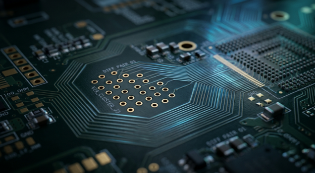
The problem is that as data rates go past a few gigabits per second, the via ceases to be a hole and becomes a real circuit element. It has its own capacitance, inductance, and – oops, worst of all, a leftover copper stub that can ring like a tuning fork! To get a board to pass DRC is only part of the success; to get a board to work at speed is to understand Signal Transition behavior. Today, we'll go over what signal transitions are, how bad signal transitions affect your performance, and the real-world techniques of designing and manufacturing clean signal transitions. For routing DDR4, PCIe, or a high-speed SerDes link, these rules are directly relevant to your next multi-layer board.
What Signal Transition Means in PCB Design
Definition and Why Signal Transitions Are Critical in Multi-Layer Boards
A signal crossing a connector, a plane split, or a package boundary, or a signal crossing between PCB layers (usually by a via) is considered a signal transition. It's just the electrical "handoff," from one transmission line to another, in layman's terms. A properly designed microstrip or stripline will maintain a fixed impedance, usually 50 ohms single-ended or 90-100 differential ohms, on a single reference plane. As soon as your signal passes through a via, that nice geometry is disturbed.
The via causes a lumped discontinuity; the return current was previously flowing cleanly on the reference plane immediately below the trace, but now it has to find a new route on a different plane! It's all about the return current issue. Always signal and return are moving together; if the signal changes layers, the return changes layers as well. It's a smooth transition if you provide a simple path. When you make a detour, you get inductance, radiation, and reflections. That's where the concept of PCB Signal Transition becomes a true one: treating both the forward path and return path as one system.
Common Challenges During Layer Changes
The schematic makes it look like a minor issue, but layer changes present a number of different issues. Each one has a different effect on signal integrity.
- Return path discontinuity: It means that the signal switches to a layer that is referenced against a different plane; the return current will no longer pass through the same via.
- Stub resonance: The unused part of a through-hole via can resonate at high frequencies.
- Impedance mismatch: The capacitance and inductance of the via are seldom equal to those of the trace, resulting in a bump to be traversed by the signal.
If any of these are wrong, then the transition is the poorest part of a great channel. Luckily, each of them can be easily fixed, and we will discuss them later.
The Impact of Poor Signal Transitions on Performance
Reflections, Crosstalk, and Signal Degradation
At a via, when a signal encounters an impedance discontinuity, some of the energy reflects back to the source. The bigger the mismatch, the larger that reflection will be: if that via is reduced to 35 ohms on a 50 ohm line, a large enough percentage of that wave will be reflected to be meaningful. These reflections act directly on your timing & voltage margin. Reflections are not the only problem. A messy transition radiates fields into adjacent structures and couples energy into adjacent vias and traces as crosstalk.
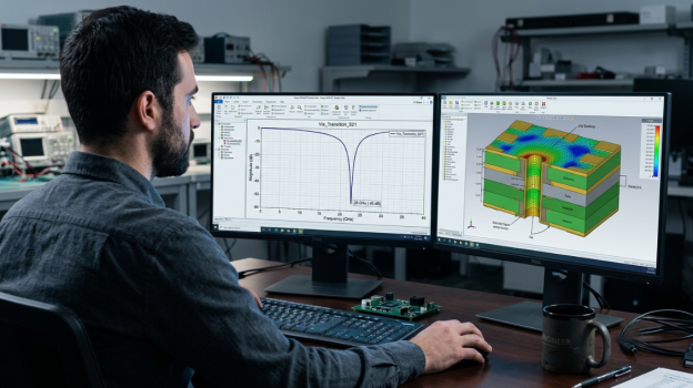
In a dense via field, such as a BGA breakout, the poor management of the transitions becomes a noise source that pollutes all of the surrounding nets. A thick board that has an unbackdrilled via through it has a copper stub that hangs down from the exit layer. This stub acts like a quarter-wave resonator, and it will produce a deep insertion loss notch (S21) at its resonant frequency. Gutting the signal at the point where it is needed, for a 1.6 mm board, a full-length stub can resonate well within the band of a 10+ Gbps link.
Effects on Timing, EMI, and Overall System Reliability
The impacts affect the entire system. The received waveform is distorted by reflections and resonant notches, which will close the eye diagram and increase jitter. That immediately reduces your timing budget on interfaces such as DDR, where every picosecond of the setup/hold window matters. Also, there is an EMI cost. If the return current does not have a way to flow directly underneath the signal, then the current is spread out across the plane, creating a large current loop.
EMC's worst enemy is loops; the larger the loop, the greater the radiation and pickup. One poor transition seam can be the sole cause that your product does not pass CISPR 32 or FCC Part 15 testing. Lastly, marginal transitions do not help in having reliable systems at scale. A design that just closes its eyes in the lab on golden boards may fail when it is manufactured, across manufacturing tolerances, temperature, and aging. Good transition design provides you with a margin of error to cope with variation in the real world.
Key Design Techniques for Optimal Signal Transitions
Via Selection, Backdrilling, and Stub Reduction Strategies
The first lever is picking the right via. The copper stub left by a through-hole via is usually the biggest cause of high-frequency loss, and so it is a priority to avoid these stubs on thick multilayer boards.
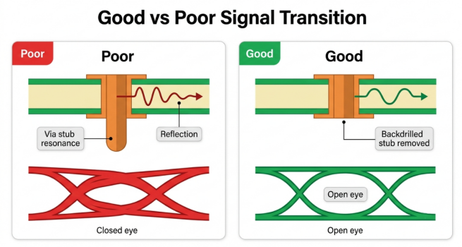
There are 3 primary methods of stub control:
- After plating, backdrilling is performed using a slightly bigger drill, which removes the unused portion of the copper barrel from the via, leaving only the portion used for the signal. This is the classic solution for signals > 5-10Gbps on thick boards, and usually results in a small controlled stub.
- Blind and buried vias: These only connect the layers required; no stub is created. They're more expensive but best for HDI and dense designs.
- Microvias are vias (typically 100-150 µm), which are made with lasers and span only one dielectric layer, providing near ideal transitions with minimal stub in HDI stacks.
A rule of thumb: If a stub is longer than about a quarter wave at the highest frequency of interest of your signal, it must be dealt with. If you backdrill down to a stub about 0.2 mm or less, the resonance is typically pushed well outside of your operating band.
Impedance Matching and Reference Plane Continuity
Even if the stub is handled, the via itself will need to be tuned to the desired impedance. The dominant knob here is the antipad, and the clearance in the reference planes around the via barrel. The bigger the antipad, the lower the capacitance of the via, and the higher its impedance, and vice versa. With field-solver-based tuning, you can tune the via to be around 50 ohms or to your differential target.
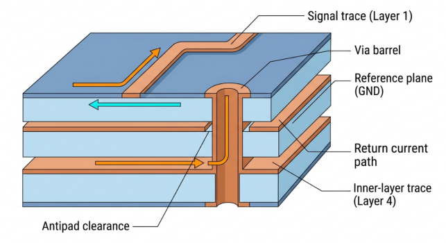
Continuity of the reference planes is also very important. The cleanest transition is where the signal stays in the same plane, or in the case of two planes with the same DC signal, they are tied together right at the via. If the signal is changing planes, you will have to provide a low-inductance path across for the return current:
- When both reference planes are grounds, position stitching vias next to the signal via, ensuring that the return current path has a straight path.
- Don't use plain stitching if the signal switches from a ground plane to a power plane (different voltages); use a stitching capacitor that is placed directly at the crossing point of the signal and carry the AC return current across.
Avoid routing a high-speed signal so that its return bit must travel over a plane split or slot (a long detour and the undoing of all your work to get the impedances right).
Layer Transition Planning for High-Speed Signals
Most transition headaches can be avoided with smart planning up front. Design your stackup so that signals are likely to use adjacent, same voltage reference planes, wherever possible. This minimizes the length and predictability of return paths. Keep the number of layer changes down on your most important nets because each change is a chance of degradation. If a transition is a must, plan for the space for the conductive stitching, or capacitors, early on, and not after the routing is locked. When transitions are created as first-class citizens of the stackup, rather than as afterthoughts, this is the sign of a mature high-speed design.
Advanced Considerations for Complex Designs
Differential Pairs, High-Frequency Signals, and Via Optimization
Differential pairs require additional attention at transitions as both vias need to be balanced. Any asymmetry results in common-mode noise that radiates and pollutes the signal, which is differential energy. One popular strategy is the GSSG (Ground-Signal-Signal-Ground) via pattern, where the two signal vias are surrounded by two ground vias, providing each signal via half with a close return path. This structure reduces the differential impedance while providing the transition with a huge common-mode rejection ratio.
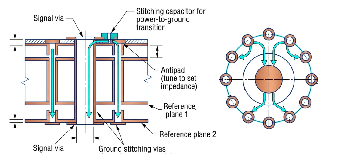
Even better isolation for very high-frequency links can be obtained if a complete via fence or a coplanar-waveguide-type ground ring encircles the transition. Here, the frequency range is important. Some semiformal rules-of-thumb in the industry: signals below about 3 GHz should be connected to a nearby ground return when crossing the layers of a plane, and signals above 5 GHz require a carefully sized antipad as well as an array of stitching vias around the transition. At frequencies higher than about 30 GHz, via inductance is so predominant that many designs strive to reduce the number of vias to a minimum.
Simulation and Analysis Methods for Transition Validation
These effects can't be eyeballed; they have to be validated by valid tools via transitions. Simple 2D impedance calculators ignore the 3D reality of a via and only take a uniform transmission line into account. The industry standard workflow utilizes 3D electromagnetic (EM) field solvers to simulate the actual via shape, antipad, stub, and stitching structure. From there, engineers refer to:
- S-parameters: insertion loss (S21) will show stub resonance notches, return loss (S11) will indicate the via impedance matching.
- TDR (Time Domain Reflectometry): Graphs impedance over distance, where you can see a dip or bump in the signal path at the via and can tune it out.
- Eye diagrams: End-to-end check for adequate margin for the desired BER.
Simulating before fabrication is much less expensive than a respin. Weeks of debugging a board that, for some reason, fails to work at speed can be avoided by a few hours in an EM solver.
Manufacturing Aspects That Influence Signal Transition Quality
Via Plating, Registration Accuracy, and Process Control
Perfect transition design still requires the fab shop that will create it well. Quality of the barrel via plating determines whether the barrel has smooth, uniform copper or voids (or thin plating), which can alter the local impedance and result in outright failures. Accuracy of registration (how well each layer matches up with the others) is important for antipad tuning. When the drilled via deviates from the antipad, there is an imbalance of clearance, which will affect impedance balance and, for differential pairs, create skew between the two halves of the pair.
Tight registration maintains the designed geometry throughout the entire stackup. Backdrilling itself is a controlled process with actual tolerances involved. Process control of the depth of the drill will determine the amount of stub left behind because the depth must be great enough to clear the stub from the hole, but not so great as to reach the last active layer.
How Fabrication Precision Affects Real-World Performance
Fabrication tolerance is the difference between the simulated and actual world. Impedance control specs typically give some tolerances, often plus or minus 10%, and a good fab shop keeps all the channels, including the via transitions, within those tolerances.
Think about how pieces will sit in practice:
| Transition Technique | Problem It Solves | When To Use It |
|---|---|---|
| Ground stitching via | Return path for signal crossing two ground planes | Any layer change between the same-voltage planes |
| Stitching capacitor | AC return path across the power-to-ground plane change | Signal references shift between different DC voltages |
| Backdrilling | Removes resonant via stub | Thick boards, signals above ~5–10 Gbps |
| Blind/buried via | Eliminates stub entirely, saves space | HDI and dense designs |
| Antipad tuning | Corrects via impedance toward the target | Any controlled-impedance transition |
If all three factors: registration, plating, and drill depth are strictly controlled, then the board you've just created will be identical to the simulated board, and your painstakingly designed board transitions will work in the field!
JLCPCB's Expertise in High-Quality Signal Transition Implementation
Advanced DFM Review Focused on High-Speed Transitions
Great transition design and great fabrication must meet in the middle, and that's where JLCPCB's process comes in. They have automated Design For Manufacturability (DFM) checks that alert the user to potential problems, such as undersized antipads or vias too near the edges of the planes, before they are manufactured, and therefore cheap to correct. JLCPCB supports controlled impedance for high-speed applications with field-solver backed stackups, making your via and trace geometry modeled, not guessed. They have a standard deviation of plus or minus 10%, which is the tolerance range of a typical transition design that must be maintained across production.
Precision Via Processing and Layer Registration Capabilities
The manufacturing is consistent with the techniques that we discussed. JLCPCB offers backdrilling for multilayer boards, which serves to knock out the via stubs, via-in-pad for near-ideal single-layer board transitions on dense stacks, and HDI microvia. Differential vias will be symmetric, and your antipads will be centered, maintaining the geometry assumed by your EM simulation. This, in conjunction with the clean and uniform via plating, is what allows a designed 50 ohm transition to measure 50 ohms on the resulting board.
Reliable Manufacturing Ensuring Consistent Signal Integrity at Scale
The last piece is consistency. What works on one prototype should work on ten thousand production units, and that takes control of the process: control in plating, control in drilling, control in lamination. When it's time to implement these principles, JLCPCB's controlled-impedance service, backdrilling, and instant quoting make it easy to get from a simulated stackup to boards you can rely on at speed. The result is high-speed hardware, with your PCB vias and layer changes no longer crippling your system, but just another well-behaved member of the channel.
FAQ about Signal Transition
Q: What is a signal transition in a PCB?
A signal transition is any point where a high-speed signal changes its routing environment, most often when it moves between PCB layers through a via. At high data rates, the via becomes a real circuit element with its own capacitance, inductance, and stub, so the transition must be designed carefully to preserve signal integrity.
Q: Why do via stubs hurt high-speed signals?
The unused copper barrel of a through-hole via acts as an open-ended quarter-wave resonator. At its resonant frequency, it creates a deep notch in the insertion loss, which can fall right inside the band of a 10+ Gbps link and severely degrade the signal.
Q: When should I use backdrilling versus blind or buried vias?
Backdrilling is the common choice for thick multilayer boards, removing the stub after plating on signals above roughly 5–10 Gbps. Blind and buried vias avoid forming a stub at all and are preferred for HDI and space-constrained designs, though they generally cost more.
Q: How do I keep the return current path clean at a layer change?
Place ground stitching vias right next to the signal via when both reference planes are ground. If the signal transitions between planes at different voltages, use a stitching capacitor at the transition instead, and never route the signal so its return has to cross a plane split.
Q: What impedance tolerance should I expect for controlled-impedance transitions?
A typical controlled-impedance specification allows about ±10% around the target value. Manufacturers like JLCPCB use field-solver-backed stackups to hold traces and via transitions inside that window across production.
Conclusion
The silent but deadly serious moments in every high-speed board are signal transitions. But a via that switches from one layer to another should not only be treated as a hole. It's a small transmission line too, and should be treated as such, or the margin will be devoured by reflections, stub resonance, and stray return currents. The correct via selection and backdrilling, antipad tuning, stitching vias or capacitors, and continuous reference planes convert a potential weak point to a clean handoff.
The more you practice the discipline around transition today, the more crucial it will be tomorrow as data rates continue to rise towards 112 Gbps PAM4 and beyond. Plan their design, rigorously test them in a 3-D field solver, and have a fabricator that is registered, plated, and can control impedance to actually produce the geometry you designed. Do that, and your PCB Signal Transition strategy is a competitive advantage, not a debugging nightmare.

Popular Articles
Keep Learning
Getting PCB Characteristic Impedance Right for Reliable Signals
Key Takeaways Impedance Defined: Characteristic impedance is set by trace geometry and the reference plane, not by copper DC resistance. Core Factors: Trace width, copper thickness, dielectric height, and dielectric constant determine the impedance value. Reference Plane: High speed traces need a continuous reference plane to prevent signal reflection. Factory Verification: Fabricators adjust trace width and check impedance using time domain reflectometry on test coupons. Design Approach: Select a sta......
Stop PCB Crosstalk Before It Becomes a Signal Integrity Problem
Key Takeaways NEXT vs FEXT: NEXT saturates with trace length, while FEXT grows linearly with distance. Spacing & Stackup: Apply the 3W rule and keep traces close to reference planes. Edge Rates: Fast rise times drive crosstalk more than clock frequency. Fab Margins: Etching variations reduce gaps, requiring extra layout clearance. Verification: Use DFM checks and TDR coupons instead of basic continuity tests. PCB crosstalk is the noise one trace pushes into its neighbor, even though the two nets are e......
Navigating the Impedance Landscape: Selecting the Right Impedance for USB, Ethernet, HDMI, and SD Card Interfaces
Introduction In the realm of high-speed digital communication, choosing the right impedance is a critical aspect of successful PCB design. Impedance matching ensures optimal signal integrity, minimizes reflections, and enhances the overall performance of interfaces such as USB, Ethernet, HDMI, and SD Card. In this blog post, we'll explore the importance of impedance, the factors influencing impedance selection, and best practices for ensuring reliable data transmission in these widely used interfaces.......
A Beginners Guide to Impedance Control in PCBs
When a digital signal is transmitted from one point to another, it causes a change in the state of the signal line. This change can be understood as an electromagnetic wave moving through the circuit. Reflection occurs when this wave encounters a boundary between different mediums. At this boundary, some of the wave's energy continues as a signal, while the rest is reflected. This process repeats until the energy is either absorbed by the circuit or dissipated into the environment. For electrical engi......
What is PCB Signal Attenuation: How Signals Weaken Over Distance and How to Mitigate It
Key Takeaways Primary Causes: Signal attenuation is mainly caused by skin effect (conductor loss) and substrate energy absorption (dielectric loss). How to Mitigate: Reduce loss by using wider traces, low-loss materials, controlled impedance, and removing via stubs. JLCPCB Solutions: JLCPCB offers Rogers high-frequency laminates, High-TG FR4, precision impedance control, and backdrilling to protect signal integrity. As a signal travels from the source to the load through PCB conductors, the signal is ......
Understanding Analog and Digital Ground in PCB Design
When working on printed circuit board (PCB) design, proper grounding is crucial for ensuring signal integrity, minimizing noise, and maintaining reliable performance. Two common types of ground planes used in PCB layouts are Analog and Digital ground. In this article, we will explore the differences between analog and digital ground, their significance in PCB design, and best practices for their implementation. Analog Ground vs. Digital Ground Analog ground and digital ground have separate purposes in......