PCB Delamination Explained: Causes, Detection, and Prevention
15 min
- What Is PCB Delamination?
- Causes of PCB Delamination
- PCB Delamination Signs and Detection
- How to Prevent PCB Delamination
- PCB Delamination Prevention and Fixes
- How Professional PCB Manufacturing Reduces Delamination Risk
- FAQs About PCB Delamination
- Conclusion
Key Takeaways
- Causes: Moisture turns into steam during 260C reflow, causing layer separation under thermal expansion.
- Materials: High-temp lead-free builds require mid/high-Tg laminates instead of standard FR4.
- Detection: Surface blisters are visual, while internal voids need acoustic testing or microsectioning.
- Prevention: Protect bond strength using balanced copper, proper press profiles, and dry packaging.
- Fixes: Epoxy repair only works on minor surface defects; internal splits require board replacement.
PCB delamination usually starts with water that the board absorbed before it was ever soldered. Near the 260 °C ceiling of a lead-free reflow profile, water begins to boil at about 46 times atmospheric pressure. Only a thin film of cured epoxy holds your layers together against it. A multilayer board consists of copper foil and glass cloth bonded with epoxy, and the epoxy is the weakest member. Copper and glass barely grow when heated. The resin expands far faster through the board's thickness because no glass fibers run that way to restrain it.
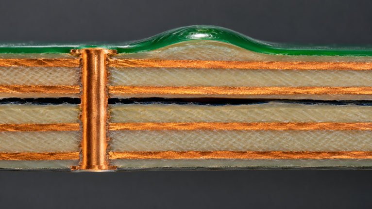
Figure 1: Multilayer PCB cross-section with a delaminated prepreg layer
Every soldering pass, therefore, pulls on the same bonds, while moisture pushes on them from the inside. Delamination is the moment one bond lets go. That is why a board can pass incoming inspection and still fail on its second trip through the oven. This guide covers how the separation starts, what causes it, and how to find it. It also covers the controls that prevent it, and when a delaminated board can be repaired.
What Is PCB Delamination?
PCB delamination is a bond failure, not a material failure. The copper, glass, and resin usually survive intact, while the interface between them lets go, so where that interface sits determines how visible the damage is.
How PCB Delamination Occurs
PCB delamination is the separation of layers in a circuit board: between laminate plies, between laminate and copper foil, or between prepreg and the inner core. IPC-T-50 calls a local, raised form of it a blister. Both begin when the stress at an interface exceeds the resin bond's capacity.
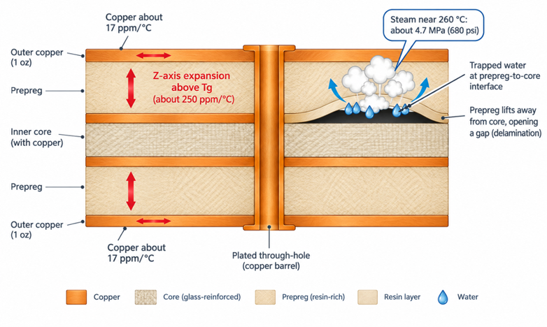
Figure 2: Thickness expansion and steam pressure acting on a prepreg-to-core bond
Most of that stress comes from heat. Glass cloth holds in-plane expansion near copper's 17 ppm/°C, but nothing reinforces the thickness direction. Above the glass transition temperature (Tg), where the resin softens, standard FR-4 expands around 250 ppm/°C through its thickness, so every hot process pulls the layers apart.
Why PCB Delamination Matters
A delaminated board can still pass a continuity test, making the defect costly to detect. The void is an insulator, so every net stays connected. But the plated holes crossing it lose support, so each thermal cycle strains the barrel until it cracks open intermittently in the field.
The void also changes the board electrically. Air has a dielectric constant of 1.0 against roughly 4.4 for FR-4, so traces above the gap shift in impedance. Moisture that collects in the separation allows a conductive anodic filament (CAF), a copper growth along debonded glass fibers, to bridge neighboring holes.
Causes of PCB Delamination
Delamination has three root sources, and they usually act together. Weak material or lamination leaves the bond fragile, subjecting it to moisture and heat load, and drilling or layout choices concentrate that load.
Material and Lamination Issues
The resin system sets how much heat a bond can survive. Standard FR-4 is cured with dicyandiamide (dicy), which absorbs more water and decomposes earlier than phenolic-cured lead-free systems. IPC-4101 slash sheets capture that difference through decomposition temperature (Td) and time to delamination at 260 °C and 288 °C (T260 and T288).
| IPC-4101 Slash Sheet | Minimum Tg / Td | Minimum T260 / T288 | What It Means for Delamination |
|---|---|---|---|
| /21, standard FR-4 | 110 °C / not specified | Not specified | No guaranteed lead-free margin, so limit it to simple single-pass builds |
| /99, mid-Tg lead-free | 150 °C / 325 °C | 30 min / 5 min | Rated for lead-free reflow, the usual floor for double-sided assembly |
| /126, high-Tg lead-free | 170 °C / 340 °C | 30 min / 15 min | For thick multilayers, many reflow passes or planned rework are required |
Moisture and Thermal Stress
Epoxy is hygroscopic, so a bare board absorbs water from the air from the day it ships. How much water a board can tolerate depends on its resin system, construction, and soldering temperatures, so no single limit applies to every design.
Water at an interface flashes to steam during reflow, and saturated steam at 260 °C sits near 4.7 MPa (680 psi). A sound bond resists that pressure. A bond already weakened by heat or a poor press cycle splits, which is how most assembly-stage blisters form.
Heat loads the bond even when the board is dry. Every pass above Tg drives the resin through its large thickness expansion, so each pass adds a stress cycle. Two reflows, a wave pass, and rework each spend some margin, so failures often appear at the last process rather than the hottest.
Manufacturing and Design Factors
Drilling can start a separation in a laminate that was bonded correctly. A dull or overheated bit pushes through the glass instead of cutting it, which cracks the resin around the hole into a pale ring called haloing. Plating chemistry can then wick into those cracks, so a clean-looking hole opens into a delamination path at reflow.
Layout decides where stress concentrates, and copper balance is the first lever. An inner layer with large empty areas causes prepreg resin to spread farther, leaving resin-starved zones where the bond is weakest. Even coverage on every layer pair, as this guide to copper pour basics explains, removes those zones.
PCB Delamination Signs and Detection
Surface delamination usually announces itself, whereas internal delamination must be found on purpose. The first needs a trained eye, and the second needs a test that sees through the board or cuts it open.
Common Signs of PCB Delamination
Delamination that reaches the surface shows up in four ways, listed from easiest to hardest to spot. Each point leads to a different depth, so the sign also tells you where to look next.
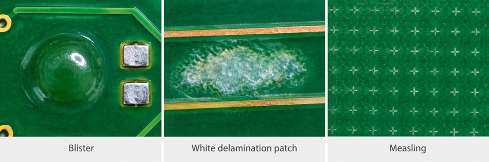
Figure 3: A blister, a white delamination patch, and measles compared
- Blisters: raised, rounded bumps in the laminate or beneath the solder mask, typically observed immediately after reflow.
- White spots and patches: lighter zones where resin has pulled away from the glass, most visible when light shines through the board.
- New bow or twist: a board that was flat before soldering comes out warped, because a released layer no longer restrains its neighbors.
- Lifted pads and intermittent faults: pads that peel during rework, or openings that come and go with temperature, pointing deep into the stack.
Measling is the sign most often mistaken for delamination. It shows as small white crosses where glass fibers have separated at the weave intersections. IPC-A-600 accepts it far more readily than blistering, because it rarely affects reliability. A microsection settles which one it is because delamination separates plies or lifts the copper foil from the laminate, while measling remains at the weave intersections.
Methods for Detecting Internal Delamination
Three methods cover most internal inspection work. They differ in what they sacrifice: the board, a coupon, or a sample of raw laminate.
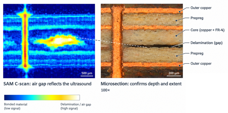
Figure 4: Acoustic microscopy C-scan of a delaminated board next to the matching microsection
- Scanning acoustic microscopy (SAM): an ultrasonic transducer scans the board underwater, and any air gap reflects nearly all the sound, so voids show as bright areas.
- Thermal stress and microsection: a coupon floats on 288 °C solder for 10 seconds under IPC-TM-650 method 2.6.8, then is cut, polished, and examined for separations.
- Time to delamination by TMA: a thermomechanical analyzer holds the laminate at 260 °C or 288 °C and records the minutes until it separates, per IPC-TM-650 method 2.4.24.1.
X-ray, the usual tool for hidden joints, is a poor fit here. A thin air gap barely changes how much radiation passes through, whereas it reflects almost all of an ultrasonic pulse. That is why acoustic microscopy, not X-ray, is the screening tool for delamination.
How to Prevent PCB Delamination
Prevention works through the same three causes in reverse. Keep water out of the materials, give the bond a full press cycle, and limit drilling and thermal damage to the board.
Control Materials and Moisture
Material choice comes first, because it sets the margin that every later step spends. A board facing lead-free reflow on both sides, or any rework, belongs on IPC-4101/99 or /126 laminate rather than unspecified FR-4. This guide to selecting the Tg of a PCB covers the trade-offs for thick multilayers. Moisture control protects that margin. Fabricators store prepreg and cores in climate-controlled rooms, and finished boards should ship vacuum sealed with desiccant and a humidity indicator card, whose spots change color as humidity rises. Once the bag is opened, the board reabsorbs water, so plan assembly within days.
Optimize Lamination Processes
Lamination must remove air, water, and contaminants before the resin cures. Vacuum pulls trapped air and moisture out before the resin flows. The heat-up rate must stay within the window specified in the laminate maker's process guide, as it determines how far the melted prepreg flows before it gels. Too little flow leaves dry spots that fail at reflow.
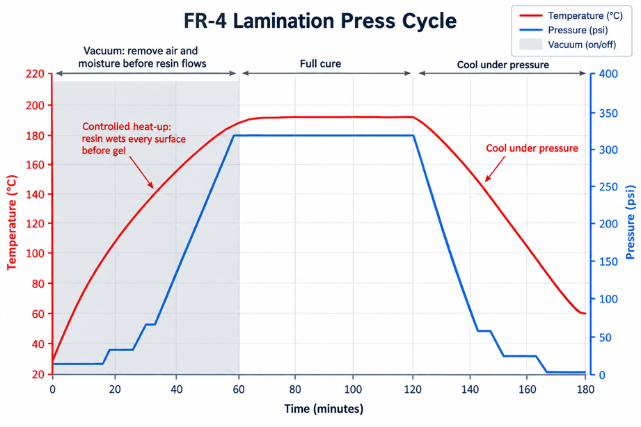
Figure 5: FR-4 lamination press cycle with temperature, pressure, and vacuum over time
Inner-layer copper preparation matters as much as the press. A brown oxide or oxide-alternative treatment etches a rough surface that the resin locks into. The treated cores must then be laid up within a short window, before they pick up moisture or handling contamination.
Control Drilling and Thermal Processes
Drilling damage is controlled with sharp tools and proper support. Fabricators cap the hits per drill bit and set feeds and speeds so the bit cuts rather than rubs. An aluminum entry sheet and a backup board sandwich the panel, so the exit side cannot split outward.
| Process Step | Typical Peak Temperature | Exposure | What to Control |
|---|---|---|---|
| Lamination press | 180 to 200 °C | 60 to 120 min | The fabricator's profile, since this step builds the bond |
| Lead-free HASL | 250 to 265 °C | Seconds, as a dip | Choose ENIG or OSP on thick boards to skip the shock |
| Lead-free reflow (SAC305) | 240 to 250 °C | 60 to 90 s above liquidus | Use the paste's required peak, not the 260 °C ceiling |
| Wave soldering | 255 to 265 °C | Seconds per pass | Count it as one more cycle against the margin |
| Hot-air rework | 300 °C or more, locally | Tens of seconds | Preheat from below and limit attempts per site |
PCB Delamination Prevention and Fixes
Once a board has delaminated, the question becomes containment. You either seal damage that is small, shallow, and stable, or scrap a board that cannot survive its next thermal cycle.
Can Delaminated PCBs Be Repaired?
A delaminated PCB can be repaired only when the separation is small, near the surface, and clear of conductors. In that case, IPC-7711/7721 describes an injection method. Small holes are drilled into the void; low-viscosity epoxy is injected through one while another vents air, and the cured epoxy seals the area.
The limits are tight because epoxy only fills voids that a drill can reach without cutting copper. Inner-layer separation and damage around plated holes are out of reach. Injected resin also fails to restore either the barrel support or the original dielectric. So treat repair as a way to stabilize a prototype, and expect high-reliability contracts to require customer approval first.
When Should a PCB Be Replaced?
Replace the board whenever delamination fails to meet IPC-A-600 limits, contacts copper structures, or continues to grow. For Class 2 and 3 boards, the standard accepts it only within 1% of the board area on each side. It must also span no more than 25% of the gap between adjacent conductors and must not grow under thermal testing.
| What You Find | Why It Matters | What to Do |
|---|---|---|
| Small surface blister away from conductors, within IPC-A-600 limits | Shallow and stable | Accept, or seal by epoxy injection |
| Blister spanning over 25% of a conductor gap | Spacing is no longer guaranteed | Replace the board |
| Separation reaching a plated hole or via field | Barrels crack under thermal cycling | Replace the board |
| Inner-layer void found by SAM or microsection | Unreachable, and impedance has shifted | Replace the board |
| The same defect on several boards from one lot | Points to a material or process cause | Replace and quarantine the lot |
How Professional PCB Manufacturing Reduces Delamination Risk
Most delamination controls act before you see the board, so the fabricator's discipline is part of your reliability budget. Two areas matter most: control across the whole process, and verification sized to the board's complexity.
End-to-End Process Control
End-to-end control means one moisture and temperature discipline runs from the incoming laminate to the packed board. Materials are stored dry, treated cores are pressed within their window, and the press cycle is profiled for the material. A gap at any step consumes the margin built by the other steps.
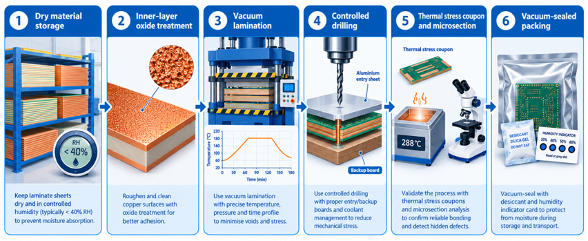
Figure 6: End-to-end delamination control from dry laminate storage to vacuum-sealed packing
JLCPCB builds rigid boards on Grade A FR-4 from Nan Ya, KB, and Shengyi, and its PCB capabilities page sets out the material choices. Its TG170 option is Shengyi S1000-2M, an IPC-4101/126 laminate whose datasheet T288 is about 30 minutes. Boards ship vacuum-sealed with a desiccant and a humidity indicator card, so the card shows on arrival whether the pack stayed dry.
Quality Control for Complex PCBs
Complex boards with high layer counts, thick stackups, or mixed materials have more interfaces and carry more heat. IPC-6012, the performance specification for rigid boards, therefore calls for coupons to be thermally stressed, microsectioned, and evaluated for delamination and blistering. Ordering to Class 3 tightens the sampling and the limits.
Your part is to send a board that can be built balanced and dry. That means a symmetric stackup, even copper on paired layers, the laminate grade in the fabrication notes, and the reflow and rework passes to expect. General PCB design rules and best practices cover the rest, and JLCPCB's online quote page lets you pick the Tg grade when you order.
FAQs About PCB Delamination
Q: Does a higher Tg laminate always prevent delamination?
No, because Tg only marks where the resin softens, not how long the bond survives at soldering heat. A dicy-cured high-Tg laminate can delaminate sooner than a phenolic-cured mid-Tg one. So compare Td and T260 alongside Tg.
Q: How can I tell whether the fabricator or the assembler caused the delamination?
Float unassembled boards from the same lot on 288 °C solder for 10 seconds, then section them. If they delaminate, the cause is either the material or the lamination. If bare boards pass but assembled ones fail, check moisture uptake and the number of thermal passes.
Q: Does the surface finish affect delamination risk?
Slightly, because lead-free HASL dips the whole board in molten solder at roughly 250 to 265 °C before assembly. That shock matters most on thick, high-layer-count boards. ENIG and OSP skip the dip, leaving the full margin for assembly.
Q: Can delamination start years after the board was assembled?
It can, though it usually grows from a weak bond that was already there. Power cycling and outdoor temperature swings repeatedly cause the thickness to expand and contract thousands of times, while humidity introduces moisture into the interface. So a board with little margin can separate slowly in service.
Q: Do flex and rigid-flex PCBs delaminate the same way?
The mechanism is the same, but polyimide absorbs considerably more water than FR-4, and the coverlay adhesive can trap moisture as well. So flex and rigid-flex boards should be baked shortly before reflow, once their moisture-barrier bags are opened.
Conclusion
PCB delamination is rarely caused by a single mistake. It usually results from a combination of poor material selection, moisture absorption, manufacturing issues, and repeated exposure to high temperatures. Every PCB has a limited ability to withstand thermal stress. Factors such as laminate quality, lamination conditions, and storage practices determine how well the board handles heat. Each reflow, wave soldering, or rework cycle adds stress, gradually increasing the risk of internal layers separating.
Preventing PCB delamination starts with choosing the right materials and controlling the manufacturing process. Select laminates with suitable T260 ratings, protect boards from moisture, and avoid unnecessary heating cycles. Working with a reliable manufacturer like JLCPCB, which uses controlled production processes and protective vacuum packaging, can help minimize these risks and improve long-term PCB reliability.

Keep Learning
PCB Delamination Explained: Causes, Detection, and Prevention
Key Takeaways Causes: Moisture turns into steam during 260C reflow, causing layer separation under thermal expansion. Materials: High-temp lead-free builds require mid/high-Tg laminates instead of standard FR4. Detection: Surface blisters are visual, while internal voids need acoustic testing or microsectioning. Prevention: Protect bond strength using balanced copper, proper press profiles, and dry packaging. Fixes: Epoxy repair only works on minor surface defects; internal splits require board replac......
Why PCB Test Coupons Are Critical for Reliable Board Manufacturing
Key Takeaways Sacrificial Testing: Coupons allow destructive tests without harming active boards. True Process Mirror: They match the exact stackup and density to reflect panel quality. Clean Measurements: Straight lines enable precise TDR impedance and via inspection. Quality Shield: Coupon failures isolate flawed panels before shipping. A PCB test coupon is the one piece of your order that is intentionally destroyed. It rides in the panel border beside your boards, so it sees every drill, plating, a......
How to Master PCB Impedance Testing for High-Speed Designs
Key Takeaways Verification via TDR: Impedance testing uses Time-Domain Reflectometry (TDR) on test coupons to verify high-speed traces. Real-World Factors: Actual impedance is shifted by manufacturing variables, including trace undercut, solder mask, and pressed dielectric thickness. Design-to-Fab Loop: Use the manufacturer's exact stackup Dk values for layout and TDR reports to refine revisions within $\pm 10\%$ tolerance. An impedance test can be the difference between a USB 3.0 link that works reli......
Guardians of Quality: A Complete Walkthrough of PCB Inspection Standards
Key Takeaways Layered Defense: Combining AOI, AXI, ICT, and FCT covers all inspection blind spots. Paste Printing: Solder paste causes up to 60% of defects, making early checks vital. IPC Standards: IPC Class 3 tightens BGA void limits from 25% to 10%, raising costs. Thermal Balance: Equal layout heating balances reflow pull to prevent tombstoning. Design Control: Clear test pads and visible polarity marks ensure reliable automated checks. PCB inspection is not one check performed at the end of produc......
Ensuring Superior Solderability: The Critical Role of Testing in Reliable PCB Production
Key Takeaways Core Purpose: Verifies solder wetting before assembly to prevent yield drops and joint failures. Destructive Test: Per J-STD-002, tested components and coupons cannot be reused in production. Pass Standards: Requires 95 percent solder coverage on leads and 80 percent on exposed thermal pads. Key Defects: Catches non-wetting (exposed metal), dewetting (solder pulling back), and black pad on ENIG. DFM Prevention: Use thermal relief, keep silkscreen off pads, and select the right surface fi......
Solder Joint Inspection in PCB Manufacturing : A Complete Guide to Catching Defects Early
Key Takeaways Solder Joint Inspection is critical in modern PCB manufacturing to catch defects early and ensure product reliability. By combining Solder Paste Inspection (SPI), 3D AOI for visible joints, and X-ray for hidden BGA/QFN issues, manufacturers can effectively detect common defects such as bridging, cold joints, tombstoning, and head-in-pillow. Following IPC-A-610 standards with a layered inspection strategy significantly reduces field failures while improving first-pass yield. JLCPCB’s prof......