
Copper Balancing in PCBs: Achieving Optimal Performance and High Yields with JLCPCB
12 min
- What is Copper Balancing and Why Modern PCBs Depend on It
- Key Fabrication Factors Affecting Copper Balance
- Best Practices for Copper Balancing in PCB Design
- Advanced Manufacturing Techniques for Superior Copper Balancing
- FAQ about Copper Balancing in PCBs
Key Takeaways
- Copper balancing strategically distributes copper across PCB layers to create uniform density, preventing warpage, uneven plating, inconsistent etching, and signal integrity issues.
- The ideal copper density target sits within the 40%–60% golden ratio, with mirrored layers maintaining density variation within 15%–20% per IPC-6012 standards.
- Copper thieving (dot patterns or crosshatch meshes) equalizes current density during electroplating without introducing parasitic capacitance on sparse signal layers.
- JLCPCB integrates copper balancing into automated DFM checks and panel-level fabrication, achieving warpage under 0.5% for high-reliability sectors.
- Common pitfalls include ignoring internal layer vacuums, placing thieving too close to high-speed traces (3W Rule), and leaving floating copper islands unconnected to any net.
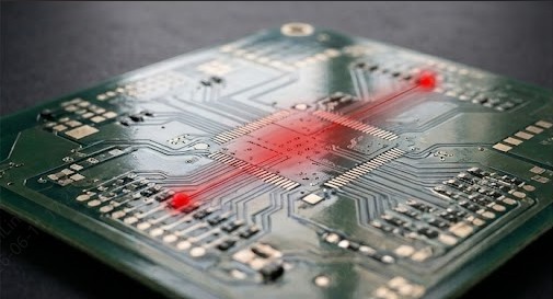
Copper balancing remains one of the most important yet frequently overlooked elements in achieving high-yield, reliable printed circuit boards. It involves strategically distributing copper across layers and within each layer to create uniform density. This prevents manufacturing defects such as board warpage, uneven plating, inconsistent etching, and signal integrity issues. At JLCPCB, we integrate copper balancing principles into our Design for Manufacturing (DFM) checks and precision fabrication processes, delivering consistent results from prototypes to volume production.
This comprehensive guide explores the principles, challenges, design best practices, and advanced manufacturing techniques behind effective copper balancing. Drawing from real-world fabrication experience and industry standards, it provides actionable insights for engineers aiming to optimize performance and reliability.
What is Copper Balancing and Why Modern PCBs Depend on It
The Core Principle of Symmetrical Layer Construction
Copper balancing relies on two pillars: achieving uniform copper coverage within each layer and ensuring a symmetrical stackup configuration around the board's centerline (neutral axis). In high-reliability designs, the ideal target copper density typically sits within the 40% – 60% golden ratio.
During fabrication, processes like lamination, electroplating, and etching react differently to high-density versus low-density copper zones:
Thermal & Chemical Stress: Drastic density gradients introduce internal stresses due to uneven heat absorption and chemical reaction rates.
The JLCPCB Approach
We combine customer-side design optimizations (such as copper pours and thieving) with panel-level adjustments to ensure absolute uniformity across the entire manufacturing panel.
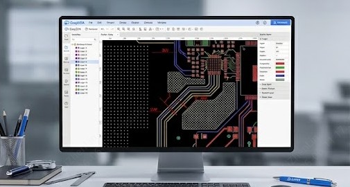
Design Advantage: Engineers utilizing tools like EasyEDA can instantly analyze layer densities and apply custom fills or grid patterns, ensuring the physical board behaves predictably through assembly thermal cycles.
Table 1: Recommended Copper Density Guidelines (JLCPCB Best Practices)
| Copper Density Range | Recommendation | Typical Applications | Expected Benefits |
|---|---|---|---|
| < 30% | Add extensive thieving | Sparse signal layers | Prevents excessive resin flow & warpage |
| 40-60% | Ideal target | Most multilayer boards | Best uniformity in plating & etching |
| 60-70% | Acceptable with care | Power/ground heavy designs | Good thermal performance |
| > 70% | Reduce or hatch pours | High current planes | Avoids etching difficulties |
The "Three Silent Killers" of Copper Imbalance
Neglecting copper uniformity directly manifests as costly assembly defects and field failures:
❶ The "Potato Chip" Effect (Board Warpage)
This is the most visible consequence of poor balancing. Because copper (CTE ≈ 17 ppm/°C) expands and contracts differently than FR-4 resin (CTE ≈ 12-16 ppm/°C), entering a 245°C-260°C reflow oven causes asymmetrical internal stress to snap.
The Consequence: Severe bow and twist.
Industry Standards: IPC-6012 mandates a maximum warpage of 0.75% for SMT boards. Unbalanced boards easily shoot up to 1.0% - 1.5%, causing pick-and-place errors, tombstoning, and open solder joints. Thin boards (< 1.0mm) and high-layer-count stackups are exceptionally vulnerable.
❷ "Out of Shape" Traces (Uneven Etching & Plating)
In chemical etching lines, the etchant fluid flows faster across sparse regions, leading to the over-etching of fine traces. Conversely, dense copper zones slow down chemical exchange, causing under-etching. This variance destroys your calculated trace width tolerances and impedance targets.
Furthermore, electroplating currents concentrate in sparse zones, causing a 20%–30% thickness variation across a panel, which degrades via reliability and solder mask adhesion.
Table 2: Impact of Copper Balancing on Manufacturing Outcomes
| Parameter | Poor Copper Balance | With Proper Copper Balancing | Improvement Noted |
|---|---|---|---|
| Plating Thickness Variation | 20-30% | <10% | Significantly more uniform |
| Board Warpage (Bow/Twist) | 1.0-1.5%+ | <0.5-0.75% | Meets or exceeds IPC-6012 |
| Trace Width Tolerance | ±1.5-2.0 mil | ±0.5-1.0 mil | Better impedance control |
| First-Pass Yield | Lower | Markedly higher | Reduced respins & costs |
| Via / PTH Reliability | Higher failure risk | Excellent under thermal stress | Improved long-term durability |
Industry Standards for Effective Copper Balancing
IPC-6012 Class 2 and Class 3 set the global benchmarks for acceptable board flatness and plating quality.
The Design Golden Rule: The overall copper density variation between mirrored layers should stay strictly within 15% – 20%.
JLCPCB Internal Controls
For high-reliability sectors (automotive, industrial control, medical), JLCPCB can achieve warpage under 0.5%. Our automated DFM analysis evaluates individual board and panel-level distribution upfront, flagging imbalances before production begins.
Key Fabrication Factors Affecting Copper Balance
Symmetrical Copper Weight & Layer Distribution
JLCPCB offers standard finished copper weights of 1oz (35µm) for outer layers, with 0.5oz/1oz/2oz options for inner layers (up to heavier weights for specialized high-power builds).
Symmetry requires mirroring copper mass around the board center core:
Physical Mirroring: Layer 1 and Layer 4 must have comparable copper weights and coverage; Layer 2 and Layer 3 must mirror each other similarly.
Heavy Copper Warning: When utilizing 2oz+ copper for high-current routing, adjacent or mirrored layers require extra attention to balancing to compensate for the massive thermal mass.
Table 3: JLCPCB Standard Copper Weight Options
| Layer Type | Available Weights | Common Use Cases | Notes |
|---|---|---|---|
| Outer Layers | 1oz (standard), 2oz | General & power boards | 2oz mainly for 2-layer |
| Inner Layers | 0.5oz, 1oz, 2oz | Multilayer designs | Depends on total layer count |
| Heavy Copper | 2.5oz–4.5oz (special) | High-current applications | Available on select builds |
Stackup Thermal Expansion Management
We support board thicknesses ranging from 0.4mm to 4.5mm. During high-temperature, high-pressure lamination, prepreg resin flows and shrinks. A balanced, symmetric stackup ensures that the coefficients of thermal expansion (CTE) are uniformly constrained, keeping the board perfectly flat during assembly reflow.
Panelization and Border Flow Pours
Often, a single PCB looks perfectly balanced, but issues arise once arrayed into a manufacturing panel. To solve this, JLCPCB adds patterned copper pours or grid blocks to handling strips, breakaway tabs, and panel borders. This equalizes current distribution during electroplating and prevents the panel from sagging during wave soldering.
Best Practices for Copper Balancing in PCB Design
Smart Use of Solid Copper Pours
Fill large, unused areas with grounded copper where electrically appropriate, ensuring proper clearances to avoid unwanted coupling.
Dual Benefits: It drastically reduces the volume of copper that must be chemically etched away (making fabrication more eco-friendly) and acts as an excellent thermal heat sink and EMC shield.
JLCPCB Process Advice
Maintain a clearance of at least 0.5mm between copper pours and high-speed differential pairs or sensitive analog lines to eliminate parasitic capacitance.
Advanced Techniques: The Art of Copper Thieving
In high-density interconnect (HDI) or high-layer multilayer boards, some signal layers might be nearly empty. Directly adding massive solid copper planes introduces unacceptable parasitic capacitance, while leaving them blank triggers plating and warpage defects.
The solution is Strategic Copper Thieving. High-speed design experts typically implement one of two classic patterned styles:
❶ The Classic Dot Pattern
Design Specs: Use solid dots with a diameter of 20-40 mil, spaced out at a 50-80 mil pitch.
Core Benefit: This is the industry-preferred choice for low-density zones because it distributes electroplating currents flawlessly without creating large solid plates.
❷ The Crosshatch Mesh
Core Benefit: Provides excellent thermal expansion balancing while drastically cutting down on parasitic capacitance underneath high-frequency routing layers.
Pitfall Alert — The 3W Rule
Regardless of your thieving pattern, ensure that the thief features stay at least 3 times the trace width away (3W Rule) from any impedance-controlled transmission lines (50 Ω single-ended or 100 Ω differential). Violating this will severely distort your trace impedance!
DRC Verification and Top Design Pitfalls to Avoid
Before exporting your production Gerber files, run a comprehensive Copper Density Report within your EDA software. Alternatively, upload your files to the free online JLCPCB DFM Analysis tool to view an instant thermal-style map of your panel's copper distribution.
Always watch out for these common engineering traps:
Common Design Pitfalls
- The "Outer-Layer-Only" Blindspot: Focusing exclusively on balancing Top/Bottom layers while ignoring massive internal layer vacuums that pull the board out of alignment.
- Thieving Encroachment: Placing thieving patterns directly against high-speed paths, resulting in sudden impedance drops and signal reflection.
- Asymmetrical Stackups: Forcing an uneven layer stackup or mismatched copper weights between mirrored layer pairs to save space.
- Floating Copper Islands: Creating isolated copper pours that do not connect to a net (like GND). These act as antennas that collect electromagnetic noise and generate structural stress concentrations.
Advanced Manufacturing Techniques for Superior Copper Balancing
Precision Etching and Uniform Copper Removal
With balanced copper density, JLCPCB can optimize etchant parameters (spray pressure, temperature, speed) for uniform results across the entire panel. This produces tighter trace width tolerances (±0.5-1.0 mil in well-balanced designs) and cleaner edges, critical for fine-pitch components and high-speed signals.
Optimized Electroplating for Consistent Thickness
Copper thieving equalizes current density during electroplating, reducing thickness variations from 20-30% to under 10%. This is particularly important for plated through-holes and vias, where uniform barrel thickness directly impacts reliability under thermal stress. JLCPCB's controlled plating lines, combined with customer balancing, deliver excellent consistency.
Material Selection and Lamination Processes to Minimize Warpage
JLCPCB uses premium FR-4 materials and controls lamination parameters (temperature ramp, pressure, cooling) meticulously. Symmetric stackups with balanced copper allow standard processes to achieve warpage under 0.5% in many cases. Thicker boards (1.6mm+) offer better inherent stability, while careful prepreg selection further reduces residual stresses.
JLCPCB's Advanced Capabilities in Copper Balancing
JLCPCB's automated DFM system reviews copper density across all layers and at the panel level. Engineering teams provide feedback when imbalances are detected, helping customers optimize designs quickly. With support for 1-32 layers, various copper weights, and fast turnaround (as quick as 24 hours for standard specs), we maintain strict quality controls including AOI and cross-section inspection to verify results. This end-to-end expertise ensures every order benefits from professional copper balancing.
FAQ about Copper Balancing in PCBs
Q: What is copper balancing in PCB design?
Copper balancing is the process of strategically distributing copper across PCB layers to achieve uniform density. It involves two pillars: uniform copper coverage within each layer and a symmetrical stackup configuration around the board's centerline. The ideal target copper density falls within the 40%–60% range.
Q: Why is copper balancing important for PCB manufacturing?
Without proper copper balancing, PCBs suffer from three major defects: board warpage (the "potato chip" effect) during reflow soldering, uneven etching that destroys trace width tolerances, and inconsistent electroplating that causes 20%–30% thickness variations. These issues lead to assembly failures, reduced yields, and field reliability problems.
Q: What are the recommended copper density ranges?
The 40%–60% range is the ideal "golden ratio" for most multilayer boards. Below 30% requires extensive copper thieving to prevent resin flow and warpage. Above 70% may cause etching difficulties and should be addressed by hatching pours. The variation between mirrored layers should stay within 15%–20% per IPC-6012 standards.
Q: What is copper thieving and when should I use it?
Copper thieving involves adding small, non-functional copper patterns (dots or crosshatch meshes) to sparse signal layers. It equalizes current density during electroplating without introducing the parasitic capacitance that solid copper planes would create. Use thieving on nearly empty signal layers in HDI or high-layer-count designs.
Q: How does JLCPCB help ensure proper copper balancing?
JLCPCB's automated DFM system reviews copper density across all layers and at the panel level before production. Engineering teams flag imbalances and provide optimization feedback. Combined with precision etching, controlled plating, and careful lamination, JLCPCB can achieve warpage under 0.5% for high-reliability applications.
Q: What is the 3W Rule for copper thieving?
The 3W Rule states that copper thieving features must stay at least 3 times the trace width away from any impedance-controlled transmission lines (such as 50 Ω single-ended or 100 Ω differential pairs). Violating this rule causes sudden impedance drops and signal reflection, severely degrading high-speed performance.
Conclusion on Copper Balancing in PCBs
Copper balancing is not an optional aesthetic addition; it is the physical foundation that keeps high-performance, dense PCBs flat, functional, and durable throughout their operational lifespans. By embracing symmetrical stacking, intelligent pours, and thieving patterns—and partnering with an expert manufacturer like JLCPCB—you can completely eliminate the nightmare of warped boards.
Take the first step toward flawless hardware today. Upload your Gerber files to JLCPCB for an instant DFM check and quotation, and experience the impact of professional manufacturing precision!
Keep Learning
Why Tolerance Analysis Is Key to Reliable and Cost-Effective PCB Production
Key Takeaways Tolerance analysis bridges CAD perfection and manufacturing variations to ensure reliable PCB assembly. Focus on critical areas: annular rings, hole tolerances, trace/space, layer registration, and solder mask alignment. Apply Worst-Case, RSS, or Monte Carlo methods for effective tolerance stack-up. Proper analysis boosts yield, cuts respins and costs — start with JLCPCB’s DFM review. Have you ever sent a board to fabrication, which appeared flawless on the computer screen, but then foun......
The Ultimate Guide to PCB Panelization: Tools and Techniques
Printed circuit boards (PCBs) are the backbone of modern electronics. One critical aspect of PCB manufacturing is panelization — the process of arranging multiple PCBs onto a single larger panel for efficient manufacturing and assembly. This technique allows multiple boards to be processed simultaneously, significantly reducing costs and improving production efficiency. In this article, we will provide a comprehensive guide to PCB panelization, covering the tools and techniques required for successful......
Castellated PCBs: Introduction and Design Requirements
With the rapid development of electronic technology, electronic products are moving towards miniaturization, portability, multi-functionality, high integration, and high reliability.Consequently, printed circuit boards (PCBs) are frequently designed to integrate pre-existing, off-the-shelf modules. For example, IoT Bluetooth modules or NB-IoT modules, which are indispensable communication modules, can be soldered onto PCBs just like chips. These carrier boards are characterized by their small size and......
Copper Balancing in PCBs: Achieving Optimal Performance and High Yields with JLCPCB
Key Takeaways Copper balancing strategically distributes copper across PCB layers to create uniform density, preventing warpage, uneven plating, inconsistent etching, and signal integrity issues. The ideal copper density target sits within the 40%–60% golden ratio, with mirrored layers maintaining density variation within 15%–20% per IPC-6012 standards. Copper thieving (dot patterns or crosshatch meshes) equalizes current density during electroplating without introducing parasitic capacitance on spars......
PCB Design : How to Resolve Short Circuit Defects Caused by HASL
Key Takeaways In high-density PCB designs, HASL frequently causes solder bridging and short circuits due to its uneven surface and molten solder flow, especially on fine-pitch and dense traces. The most effective solution is to switch to ENIG (Electroless Nickel Immersion Gold), which provides superior planarity, significantly reduces bridging risks, and improves assembly yield. By selecting ENIG for dense layouts, optimizing solder mask design, and running DFM checks, designers can effectively elimin......
Design Process of a Surface Mount PCB
Key Takeaways Mastering the surface mount PCB design process is essential for creating compact, high-density, and reliable electronic boards. This comprehensive guide walks through the complete SMT workflow — from schematic capture and component selection to optimized layout, precise routing, DRC/ERC verification, and Gerber file generation — enabling designers to achieve superior performance, better manufacturability, and cost efficiency compared to traditional through-hole methods. By following thes......