Streamlining Modern Electronic Kits with Precision Manufacturing Solutions
16 min
- What is a PCB Board Kit and Why Do Engineers Rely on It?
- Key Components and Assembly Steps in the Making of PCB Board Kits
- Commercial vs. Custom PCB Kits for Professional Applications
- Turning Prototype Kits into Production-Ready Boards with JLCPCB
- FAQ about PCB Board Kit
- Conclusion
key takeaways
- Complete Kit Essentials: A functional kit combines bare boards, components, assembly guides, test rules, and ESD packaging.
- Optimal Assembly Sequence: Solder components from shortest to tallest to keep parts seated properly during hand assembly.
- 4-Step Testing: Always check visually, test for shorts, power up with current limits, and run functional tests in order.
- Beyond Breadboards: Custom PCB kits offer solid ground planes and avoid breadboard noise/parasitics.
- Smart SMT Offloading: Pre-assemble fine-pitch parts (under 0.65 mm) at the factory and solder through-hole components by hand.
A PCB board kit arrives on your bench as a bare board, a bag of components, and an instruction sheet. Those three parts should make a working circuit. They are introduced as packs in the classroom, soldering practice boards, and demo hardware that engineering teams give away to customers.
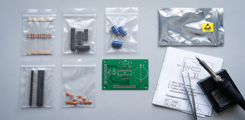
A kit is only useful when its board, bill of materials, assembly information, and test procedure agree. A footprint or polarity mismatch can turn a build into an avoidable fault. This guide explains the elements of a usable kit, the fabrication and assembly workflow, and the checks needed before a custom kit is released.
What is a PCB Board Kit and Why Do Engineers Rely on It?
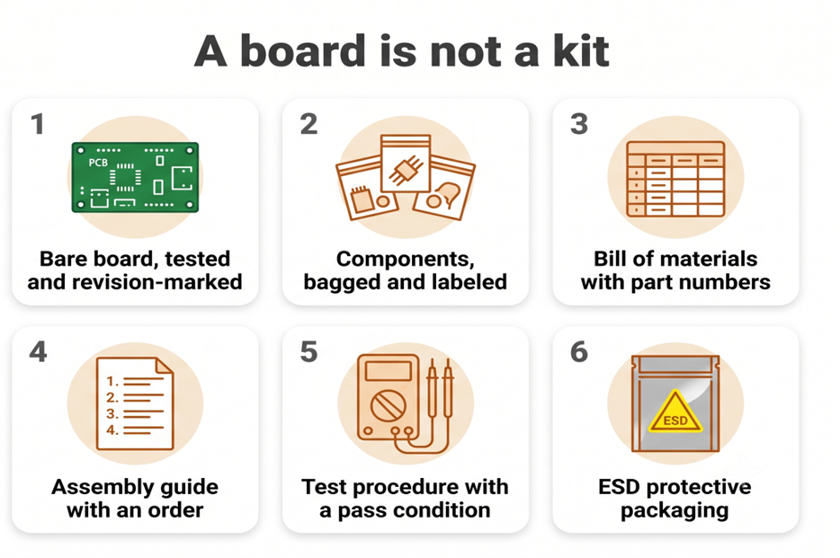
A PCB board kit is an unpopulated printed circuit board supplied with the required components and documentation showing how to assemble it. A useful kit also includes a test procedure with expected observations, so the builder can distinguish a correct assembly from a fault.
Engineers use kits because they break up two problems that are painful when done together. Circuit design is one thing, building a reliable board is another. A kit takes out the second variable; if it fails, it's a clue to your knowledge or soldering. There is no breadboard wire that is dangling and has developed a short circuit an hour ago.
Understanding the Basics of a Functional PCB Board Kit
Five things have to be in the box before a pile of parts counts as a kit. Leave one out, and the build stalls, because you cannot buy a single 0603 capacitor at nine o'clock on a Sunday evening.
- The bare fabricated board: Drilled, plated, masked, and marked, with footprints that match the exact parts supplied rather than a generic grid.
- The matched component set: Every value is in its own labeled bag or on tape, counted with one or two spares for the parts that get lost.
- The assembly documentation: A placement diagram, a bill of materials with reference designators, and a note on which parts are polarised.
- The test procedure: Expected supply current, one or two test point voltages, and a description of what a working board does.
- The consumables: Solder, flux, and wick, since a kit that assumes the builder already owns the right alloy is only half a kit.
Most kits are won or lost by documentation, as the board can only hold so much information. JLCPCB can print legend text down to 1.0 mm (40 mil) character height and 0.15 mm (6 mil) line width. That's sufficient for a reference designator, but not for a pin function or a warning.
How Hands-on Kit Integration Helps Engineers Master Circuit Design
Simulation tells you what a circuit should do, while a kit tells you what it actually does on copper. An NE555 timer running at 1 kHz behaves in SPICE exactly as the equations promise. On a real board, the same chip pulls a sharp current spike every time its output switches. That is why the 100 nF decoupling capacitor next to pin 8 stops being optional.
Building a kit connects schematic symbols to real packages, markings, assembly constraints, and verification steps. Confirm the exact package, land pattern, polarity marking, and thermal requirements from each component data sheet. Do not infer pin pitch or exposed-pad needs from another package variant of the same device.
Key Components and Assembly Steps in the Making of PCB Board Kits
Making a PCB board kit breaks down into three tasks, which are done in order. First, the bare board is fabricated, then components are ordered and soldered, and lastly, the board is tested. Failure modes vary from job to job, and if a Kit makes it through all three, then someone else can construct it without your assistance.
From Schematic to Bare Substrate: The Complete Fabrication Workflow
The bare board begins with a copper-clad laminate and goes through about 8 steps until it is delivered to you. Each one reduces the tolerance, and an error early in the chain is much more costly than an error late in the chain.
- Schematic capture and Netlist export: Draw the circuit, give a real footprint to each symbol, and export the netlist that the layout tool will enforce.
- Design Rules Check: Place, Route, and Run DRC against the real limits of the fab, not the software limits.
- Gerber and drill file output: Export the following files: one per layer, plus the Excellon drill file, and the pick and place file, if any part will be machine placed.
- CAM and DFM review: The fab checks for annular rings, mask slivers, and clearances, and flags what the process can't hold.
- Imaging and etching: The copper is covered with a photoresist and exposed through the image in the layer, then developed, and the exposed copper is etched away.
- Drilling and through-hole plating: Holes are drilled, coated with electroless copper,r and then electroplated to make the barrel conductive.
- Printing of solder mask and legend: The liquid photoimageable mask is applied and cured, and the white legend is printed over the mask.
- Surface finish, electrical test, and routing: The exposed pads are coated with HASL, ENIG, or OSP, and all nets are flying probe tested, and the boards are routed out of the panel.
Plating is the step that separates a factory board from a home-etched one, because copper does not stick to bare epoxy on its own. The drilled hole walls are first coated with a thin electroless copper film. Electroplating then builds that film up to roughly 20 to 25 um (0.8 to 1 mil) in the barrel. Without it, a through hole is only a hole, so every layer change in your kit would need a soldered wire through it.
Component Sourcing and Soldering Protocols for Reliable Hardware Assembly
Sourcing for a kit is a different exercise from sourcing for a single prototype, because you are buying for somebody else's bench. A prototype builder can substitute a 4.7 kilohm resistor for a 4.75 kilohm one and move on. A kit builder cannot, so every value in the bag has to match the value printed on the board and listed in the assembly sheet.
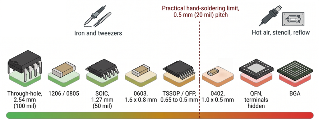
The package choice decides whether a kit can be hand-built at all. An 0805 resistor measures 2.0 by 1.25 mm (79 by 49 mil) and sits comfortably under a fine iron tip. A 0402 measures 1.0 by 0.5 mm (39 by 20 mil), which is why surface tension can pull it upright during rework. Anything a beginner will solder should stay at 0805 or larger.
| Package | Pitch or Body Size | Hand Soldering With a Fine Tip | What It Means for a Kit |
|---|---|---|---|
| DIP through-hole | 2.54 mm (100 mil) pitch | Straightforward | Safe for a first build, and a socket lets the IC be swapped |
| SOIC | 1.27 mm (50 mil) pitch | Comfortable | Drag soldering works reliably with flux and wick |
| 0805 passive | 2.0 x 1.25 mm (79 x 49 mil) | Comfortable | Tack one pad, then reflow the second |
| TSSOP | 0.65 mm (25.6 mil) pitch | Demanding | Expect bridges, so wick and flux are mandatory |
| 0402 passive | 1.0 x 0.5 mm (39 x 20 mil) | Difficult | Tombstones easily, and is better placed at the factory |
| QFN or BGA | 0.5 mm (20 mil) and below | Not practical by hand | Joints sit under the body, so a reflow and X-ray are needed |
Assembly order matters more than most kit instructions admit, because a tall part fitted early blocks the iron from everything behind it. Work outward by height, starting with resistors and diodes, then IC sockets, then ceramic capacitors, then electrolytics, and connectors last.
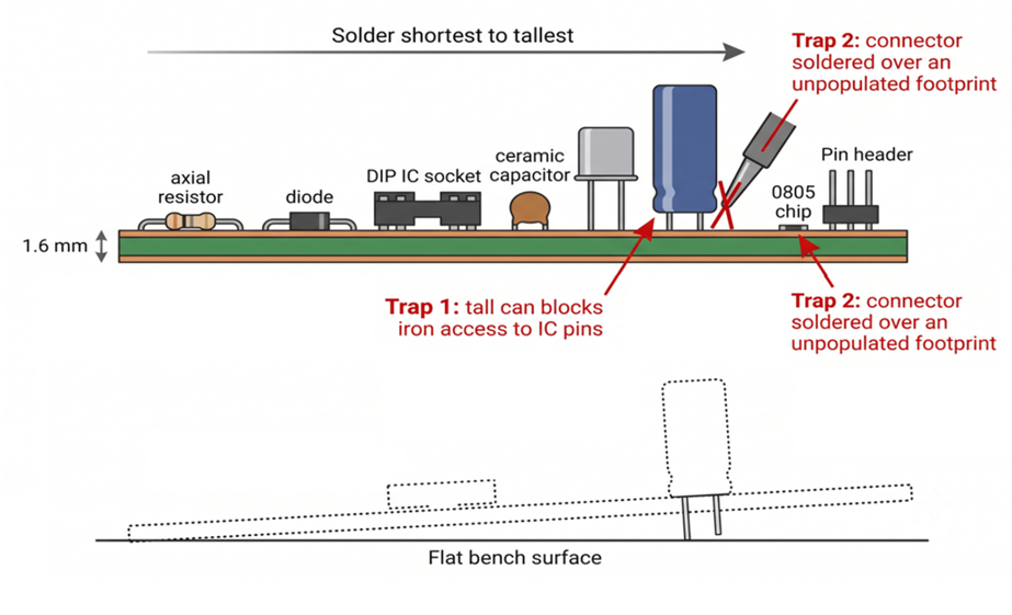
When you flip the board face down to solder, the low parts stay seated on their own. You are then not fighting gravity and a hot iron at the same time. Two traps catch almost every kit builder, and both are permanent once the solder cools. Polarity is the first, since an electrolytic capacitor, a tantalum, a diode, and an LED all look symmetrical until you check the marking.
Essential Testing Routines for Custom PCB Board Projects
Testing a kit board takes four steps, and doing them in order keeps a small fault from becoming a dead board. Skipping straight to powering up is how a single solder bridge takes the regulator with it.
- Inspect before you power anything. Look across the board at a low angle under good light, checking for bridges, missing joints, and parts fitted the wrong way round.
- Check the power rails with the supply disconnected. Measure resistance between each rail and ground, and confirm nothing reads as a short.
- Bring the board up on a current limited supply. Set the limit before you connect, then watch the current as the output is enabled.
- Run the functional test. Compare the measured test point voltages and behavior against the values written in the kit documentation.
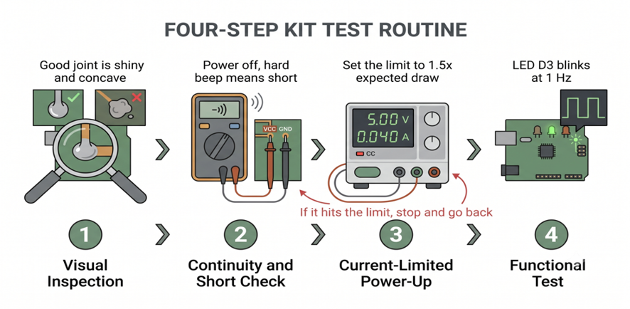
The resistance check in step two is the one that saves boards, because a solder bridge across the supply is the most common assembly fault. Measure between the positive rail and ground with the meter on its 200 ohm range. Expect anything from tens of ohms upward, depending on how much decoupling the board carries. A reading under about 1 ohm means a short, so find it before the supply does.
Commercial vs. Custom PCB Kits for Professional Applications
The difference between a commercial kit and a custom one is who chose the circuit. A commercial kit teaches a fixed lesson somebody else designed, while a custom kit is your own schematic turned into a repeatable object. Both are useful, but they stop being interchangeable as soon as your design has a requirement that the generic board cannot meet.
| Attribute | Generic Educational Starter Kit | Custom Factory-Made Kit | What It Means for You |
|---|---|---|---|
| Board construction | Single-sided FR-2, perfboard, or breadboard | 1 to 32-layer FR-4 with plated through holes | Only the custom board can carry a real ground plane |
| Circuit | Fixed, chosen by the vendor | Your own schematic | A custom kit tests your design, not somebody else's |
| Footprints | Generic 2.54 mm (100 mil) grid | Matched to the exact part number | No adaptor wiring or bent leads on the custom board |
| Solder mask and legend | Often absent | Mask plus 1.0 mm (40 mil) legend text | Fewer bridges, and the board documents itself |
| Repeatability across units | Varies with every hand etch | Outline held to ±0.1 mm (4 mil) | Fifty kits behave identically in fifty pairs of hands |
| Cost per board at five units | Low, until consumables are counted | From about $2 per order for 100 x 100 mm | Factory boards win on cost sooner than most expect |
Limitations of Generic Educational Starter Kits
Generic starter kits are built to be cheap and forgiving, and both of those goals cost you engineering fidelity. Most use a solderless breadboard or a single-sided phenolic board on a 2.54 mm (100 mil) grid. That grid works fine for a 555 blinker. It has nothing to offer a 24 MHz crystal circuit, because there is no ground plane underneath to carry the return current.
A solderless breadboard is worse than it looks on a scope. Each contact strip adds a few picofarads to every node, and each jumper adds tens of nanohenries. Edges therefore soften, and ringing appears well before 10 MHz. A circuit that works on a breadboard and then fails on a PCB is rare, while the reverse happens constantly. The parts themselves are the third limitation, because assortment kits often ship unmarked or relabelled components.
Why Professional PCB Engineers Transition to Factory-Made Custom Kits
PCB engineers move to factory-made kits when repeatability starts to matter more than turnaround. A hand-etched board is a one-off, since the etch time, the resist quality, and the drill alignment change with every attempt. A fabricated panel of twenty boards is twenty copies of one object. A fault in unit seventeen is therefore a design fault, not a process accident.
Cost is the argument that surprises people, because home etching feels free and is not. Ferric chloride, laminate, photo paper, and the hours spent scrubbing traces pass that figure quickly. The factory board also arrives with plating, solder mask, and legend already on it. Panelization is the other reason, since a kit is rarely built one at a time. Boards can be arrayed on a single panel and separated along scored lines, so both the unit price and the handling drop.
Turning Prototype Kits into Production-Ready Boards with JLCPCB
The jump from a working prototype kit to a production run is mostly a documentation exercise rather than a redesign. Your Gerbers, drill file, bill of materials, and pick and place file already describe the board completely. What changes is who builds it, so the tolerances in your design now have to match what a factory line can actually hold.
Precision Manufacturing Capabilities Tailored for Custom PCB Kits
Kit boards make specific demands on a fab because they are handled, probed, and reworked far more than a sealed product board ever is. The numbers below are JLCPCB's standard process capabilities, and each one has a direct consequence for a kit that a stranger will assemble.
| Capability | JLCPCB Standard Specification | What It Means for a Kit Board |
|---|---|---|
| Layer count | 1 to 32 layers | A four-layer kit gets a solid ground plane for clean measurements |
| Board thickness | 0.4 to 4.5 mm (16 to 177 mil) | 1.6 mm (63 mil) resists flexing while parts are pushed in |
| Minimum trace and space | 0.10 / 0.10 mm (4 / 4 mil) on 1 oz copper | Fine pitch ICs fit without escaping to extra layers |
| Track width tolerance | ±20% | Power traces need a margin, so draw them wider than the minimum |
| Minimum via drill | 0.15 mm (6 mil) | Stitching vias fit between pads without crowding the routing |
| Hole position tolerance | ±0.05 mm (2 mil) | Through-hole parts drop straight in without reaming |
| Legend text | 1.0 mm (40 mil) height, 0.15 mm (6 mil) line width | Reference designators stay readable after assembly |
| Impedance tolerance | ±10% | USB and Ethernet kit boards hold their target impedance |
Seamless One-Stop Solution: Rapid PCB Fabrication and SMT Assembly
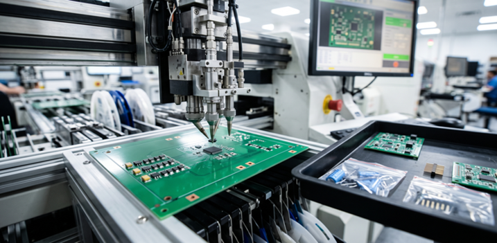
Ordering the bare board and the parts in one place removes the step where a kit usually stalls. JLCPCB carries over 720,000 components in stock. You can therefore check the bill of materials against real availability while the board is still being laid out. A part that is out of stock is one your kit builders cannot buy either. Send the fine pitch parts and the small passives to the SMT line, and leave the through-hole components, connectors, and displays in the bag. The hard joints are then already correct, while the builder still gets the satisfying part of the job.
If you are ready to move a kit design off the bench, upload your Gerbers to the JLCPCB quote page. The quote then updates live as you change layer count, thickness, and surface finish. Two-layer boards start around $2 and stencils from $6, so a full kit revision usually costs less than the parts that go on it.
FAQ about PCB Board Kit
Q:What is a PCB board kit?
A PCB board kit is a bare printed circuit board supplied with the components that populate it. Documentation and a test procedure complete the package. The board can be a simple single-sided practice board or a full four-layer design, so kits range from classroom exercises to professional demonstration hardware.
Q: Can I make a PCB board kit at home?
Yes, toner transfer onto copper clad laminate works. A ferric chloride etch then produces a usable single-sided board. It stops at around 0.3 mm (12 mil) traces and gives you no plated through holes, so anything needing two-layer routing has to go to a fab.
Q: Which components should be pre-soldered in a kit?
Anything below roughly 0.65 mm (25.6 mil) pitch is best placed at the factory. That includes 0402 and smaller passives, because those bridge faster than a hand can clear them. Leave through-hole parts, connectors, and displays for the builder, since those are the joints that are satisfying to make.
Q: What is the safest assembly order for a kit board?
Work from the lowest components upward. Start with resistors and diodes, then IC sockets, ceramic capacitors, electrolytics, and connectors last. Low parts stay seated when you turn the board over, so you are never holding a part and a hot iron at the same time.
Q: Why do cold joints appear only on the ground pads of my kit?
Ground pads connected straight into a copper pour drain heat away faster than a 40 W iron can supply it. The solder then never reaches its 183 C melting point down in the barrel. Thermal relief spokes in the layout fix this properly, while raising tip temperature is only a partial workaround.
Conclusion
A PCB board kit is worth more than the sum of its parts when it removes uncertainty rather than adding it. The board has to be fabricated to a tolerance that the builder can rely on. The parts have to be labeled and verifiable, and the test procedure has to let somebody localize their own mistake. Get those three right, and the kit teaches, because nothing in it is fighting the person building it.
Kits are also getting closer to products, since factory assembly has become cheap enough to use on a run of ten. The interesting question is no longer whether to have a kit fabricated, but where to draw the line between the machine's work and the builder's. Getting that line right is what separates a kit somebody finishes from one that ends up in a drawer.

Popular Articles
• Understanding the Basics of Electronic Devices and Circuits
• Understanding Digital Circuit Timing: Setup Time, Hold Time, Contamination Delay & Clock Skew
• PCBs Explained: A Simple Guide to Printed Circuit Boards
• Guide to the Top 10 Commonly Used Electronic Components
• Digital 101: Fundamental Building Blocks of Digital Logic Design
Keep Learning
Demystifying Bare PCB Quality for Reliability-Critical Applications
Key Takeaways Early Defect Catching: Catching faults at the bare board stage costs only the PCB, avoiding wasted components and rework later. Perfboard Risks: Zero PCBs lack reference planes and plated holes, causing signal noise above 10–20 MHz and pad lifting. Critical Material Specs: Reliability depends on hole barrel copper (20–25 µm), Tg, Td, and CTI ratings matching your operating environment. Finish & Shelf Life: HASL and ENIG last ~12 months, while OSP and Immersion Silver/Tin expire in ~6 mon......
A Comprehensive Guide to Capacitor ESR: What It Is, Good Values, and How to Measure It
Key Takeaways Definition: Capacitor ESR (equivalent series resistance) is the single resistance that represents the losses inside a real capacitor, from its electrodes, terminations, electrolyte, and dielectric. Why It Matters: Ripple current flowing through the ESR produces a ripple-voltage step on the supply rail and I²R heating in the capacitor, which limits the capacitor's ripple-current rating and service life. Conditions Matter: ESR varies with frequency, temperature, capacitance, case size, and......
Understanding IPC-6012 Standards for High-Reliability Rigid PCB Fabrication
Key Takeaways IPC-6012 vs. IPC-A-600: IPC-6012 is the binding specification, while IPC-A-600 is only for visual reference. Class 2 vs. Class 3: Class 3 requires thicker copper (25μm vs. 20μm) and zero plating voids. Coupon Verification: Quality is tested by microsectioning panel coupons after thermal stress. Upfront Callout: Specify the class on drawings upfront; boards cannot be upgraded later. IPC-6012 is the line on your fabrication drawing that decides what your supplier is allowed to ship. Most d......
Mastering PCB Plating Types and Process Control in High-Yield Fabrication
Key Takeaways Two-Step Plating: Chemical seed layer comes first, electrolytic copper adds structural strength. Process Choice: Pattern plating enables fine tracks; panel plating suits heavy copper. Via Integrity: Keep aspect ratio ≤ 10:1 to prevent thinnest-point barrel cracking. Surface Finishes: Use ENIG for flat BGA pads and hard gold for high-wear contacts. IPC Standards: Class 2 mandates 20μm copper wall thickness; Class 3 requires 25μm with zero voids. PCB plating turns a stack of drilled lamina......
Can PCB Autorouters Really Deliver Production-Ready Designs?
Key Takeaways Rules over DRC: A clean DRC only proves rules were followed, not that the board works. Placement First: Autorouters cannot compensate for bad component placement. Selective Automation: Hand-route power, analog, and high-speed traces; autoroute only repetitive or low-speed nets. DFM Validation: Verify real manufacturing tolerances before sending files to production. Every PCB autorouter sells the same promise: press one button and watch the ratlines turn into copper. On a simple two-layer......
Basic Bridge Circuits
Key Takeaways Core Principle: Bridge circuits (Wheatstone, Kelvin, H-Bridge, etc.) enable high-precision measurements and power control. Applications: Essential for sensor signal conditioning, AC/DC rectifiers, and motor drivers. JLCPCB Optimization: Maximize circuit stability with JLCPCB’s 3/3 mil traces, 4-layer stackups, and High-TG FR-4. A bridge circuit splits an input voltage into two paths, compares the voltages across different branches, and provides an output. These circuits are widely valued......