Nano-Coating vs Electropolishing for SMT Stencils
11 min
- Quick Answer: Nano-Coating vs Electropolishing Stencil
- Why Stencil Surface Finish Matters
- What Is Electropolishing?
- What Is Nano-Coating?
- Nano-Coating vs Electropolishing: Side by Side
- Do They Compete, or Combine?
- Which Do You Need? A Decision Guide
- The Data: What the Finishes Actually Change
- FAQ about Nano-Coating vs Electropolishing Stencil Finishes
- Conclusion: Match the Finish to the Board
Key Takeaways
Electropolishing improves the underlying metal surface by smoothing aperture walls.
Nano-coating adds a low-friction, hydrophobic surface that helps paste release and reduces residue.
Both treatments can improve fine-pitch paste release and support more consistent deposits and higher first-pass yield.
Nano-coating is especially useful for BGA/QFN assemblies and high-volume runs, where cleaning frequency and paste-release consistency matter more.
Electropolishing and nano-coating are complementary rather than competing treatments.
A bare laser-cut stencil can still be the practical choice for larger-pitch, low-volume work.
When ordering an SMT stencil, the order form may offer two surface-treatment upgrades, electropolishing and nano-coating. Choosing between them depends on what each treatment does and whether the application requires additional surface finishing. This nano-coating vs electropolishing stencil guide compares how the two finishes affect solder paste release, shows the key performance data, and helps you decide when each treatment is worthwhile. Electropolishing smooths laser-cut aperture walls, while nano-coating adds a low-friction, water-repelling surface. They are related but different treatments and are often used together rather than alternatives.
Quick Answer: Nano-Coating vs Electropolishing Stencil
In a nano-coating vs electropolishing stencil comparison, electropolishing smooths laser-cut aperture walls by removing micro-burrs and slag, while nano-coating adds a thin, non-stick, water-repelling layer. Both improve solder paste release in different ways, and because nano-coating performs best on a smooth wall, the two treatments are commonly combined.
Why Stencil Surface Finish Matters
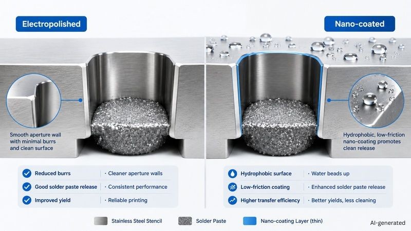
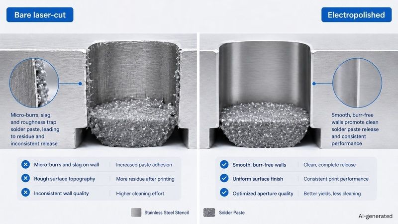
Laser cutting creates the aperture geometry that controls how solder paste is deposited, but the cut surface is not perfectly smooth. Microscopic burrs and slag can remain around the aperture edges and walls. On larger openings, these small imperfections may have little practical effect. As pitch decreases, however, there is less margin for inconsistent paste release. At fine pitches around 0.4 mm and below, rough aperture walls can retain paste and contribute to starved or inconsistent deposits, bridging, or solder balls.
That is why surface finish becomes increasingly important as aperture dimensions shrink. Good stencil design still matters, including appropriate aperture geometry and area or aspect ratios, as discussed in SMT Stencil Design Tips.
IPC-7525 provides guidance on stencil design, including aperture quality and area and aspect ratios, while IPC-A-610 defines acceptability criteria for electronic assemblies, including the consistent solder deposition expected for Class 2 and Class 3 workmanship.
What Is Electropolishing?
Electropolishing is an electrochemical surface-finishing process that removes microscopic high points from the metal. In stencil production, it is used after laser cutting to reduce burrs and slag and leave smoother, more uniform aperture walls. A smoother wall creates less mechanical resistance as solder paste separates from the stencil, which is particularly useful on fine-pitch apertures. The complete electrochemical mechanism does not need to be repeated here. For a process-level explanation, see How Electropolishing Works in a PCB Stencil.
What Is Nano-Coating?
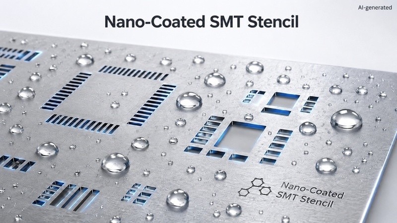
Nano-coating adds a very thin fluorosilicone polymer layer to the stencil surface and aperture walls. The resulting surface is hydrophobic and low-friction, helping solder paste release more cleanly while reducing the amount of residue left behind. This can increase the number of prints between cleaning cycles and improve stencil service life. The benefit is particularly relevant where cleaning interruptions affect throughput or where paste tends to adhere to small apertures. For a deeper look at the coating process itself, see Nano-Coated Stencil Manufacturing.
Nano-Coating vs Electropolishing: Side by Side
The following table provides a side-by-side comparison of nano-coating and electropolishing, highlighting how each treatment works, its main benefits, typical performance, and best-use applications.
| Electropolishing | Nano-Coating | |
|---|---|---|
| What It Does | Smooths aperture walls and removes burrs or slag | Adds a non-stick, water-repelling film |
| How It Works | Electrochemical material removal using anode, electrolyte, and DC current | High-vacuum deposition of a fluorosilicone polymer |
| Main Benefit | Cleaner walls and improved fine-pitch paste release | Low-friction release, fewer cleanings, and longer stencil life |
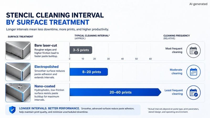
| Cleaning Interval | Can improve release and reduce residue | Typically increases from about 3-5 prints to about 20-60 prints |
| Stencil Life | Improved by better surface condition | Typical increase of about 10-30%; coating hardness around 400-450 HV |
| Surface Roughness / Precision | Smoother aperture walls | Typical Ra around 0.08-0.15 um; aperture accuracy around +/-5 um |
| Best For | Fine pitch and removal of laser-cut burrs | BGA/QFN, high-volume work, and residue-prone or no-clean pastes |
| Cost / Lead Time at JLCPCB | Low-cost surface-finish upgrade | About $4.72; roughly 12 additional production hours |
| Used Alone or Together? | Provides the smooth foundation | Performs best on an electropolished wall and is often paired with it |
Do They Compete, or Combine?
Electropolishing and nano-coating address different parts of the same paste-release problem. Electropolishing improves the stainless-steel surface by removing microscopic burrs and irregularities left by laser cutting, creating smoother aperture walls. Nano-coating works differently by adding a low-friction, non-stick layer over the metal. Because the coating performs best on an already-smooth surface, the two treatments are complementary rather than competing.
This is why many stencil manufacturers pair the two processes. At JLCPCB, electropolishing is automatically selected when nano-coating is chosen. The technical sequence is straightforward: electropolishing first improves the aperture-wall surface, then nano-coating adds the non-stick layer that supports cleaner solder paste release. The practical decision is therefore not about choosing a single winner, but about determining how much surface finishing the board requires.
Which Do You Need? A Decision Guide
The right stencil surface treatment depends on feature pitch, production volume, solder paste behavior, and how much print consistency and cleaning efficiency your process requires.
Choose a Bare Laser-Cut Stencil When:
A standard laser-cut stencil is generally sufficient for larger-pitch work around 0.5 mm and above, simple PCB assemblies, one-off prototypes, and low-volume builds. If paste is already releasing consistently and cleaning frequency is not affecting production, adding another surface treatment may provide little practical value. For general selection factors beyond surface finish, see How to Choose a Solder Paste Stencil.
Choose Electropolishing When:
Electropolishing is a practical step up when your design includes fine-pitch apertures and you want cleaner, smoother walls without paying for an additional coating. It directly addresses laser-cut burrs and surface roughness, making it a sensible option when aperture-wall quality is the primary concern.
Choose Nano-Coating When:
Nano-coating becomes more valuable for fine-pitch BGA or QFN assemblies, higher production volumes, frequent stencil-cleaning interruptions, and residue-prone or no-clean solder pastes. For QFN assemblies in particular, consistent paste release becomes increasingly important as feature dimensions shrink. Additional package and stencil considerations are covered in the Ultimate Guide to QFN Package.
Choose Both When:
For high-density, fine-pitch, or high-volume assembly, combining electropolishing with nano-coating provides both parts of the surface-treatment strategy: smooth aperture walls plus a low-friction coating. That makes the paired treatment the more complete option when print consistency and cleaning downtime matter more than minimizing stencil cost.
The Data: What the Finishes Actually Change
The value of a stencil surface treatment should ultimately show up in measurable printing behavior rather than terminology on an order form. Typical JLCPCB nano-coating figures include a surface roughness Ra of about 0.08-0.15 um, aperture accuracy of approximately +/-5 um, and coating hardness of around 400-450 HV.
Cleaning frequency can also change substantially. A conventional cleaning interval of roughly 3-5 prints may extend to around 20-60 prints with nano-coating. Typical stencil service-life improvement is listed at approximately 10-30%.
These figures show that cleaner paste separation can produce more uniform deposits and tighter solder paste inspection (SPI) consistency. More consistent deposition can reduce insufficient solder, bridging, and solder balls, helping improve first-pass yield in demanding fine-pitch assembly. For troubleshooting those issues directly, see Solder Paste Printing Defects.
The numbers should not be interpreted as guaranteed improvements on every board. Actual results depend on pitch, aperture geometry, solder paste, printer settings, cleaning practices, and production conditions. A larger-pitch prototype that already prints reliably may show little meaningful improvement.
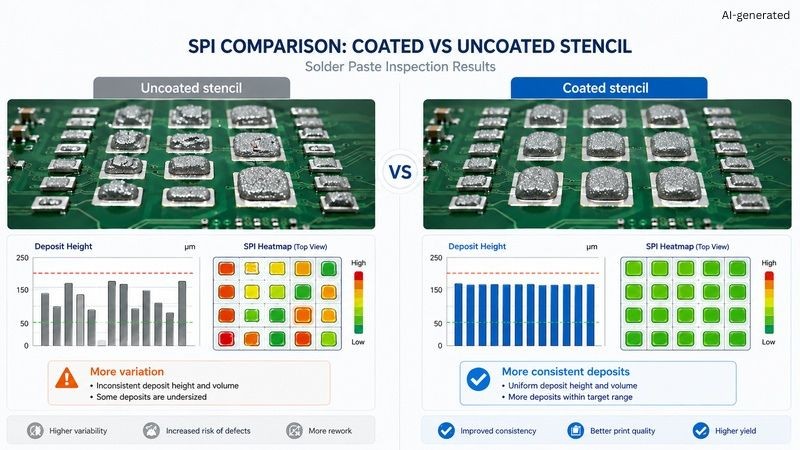
A useful evaluation is therefore to compare process data before and after the surface-treatment change. Monitor deposit consistency with SPI, note how frequently underside cleaning is required, and track whether paste-related defects decrease. For available stencil processes and manufacturing specifications, see JLCPCB's PCB stencil manufacturing capabilities.
FAQ about Nano-Coating vs Electropolishing Stencil Finishes
Can Nano-Coating Be Used Without Electropolishing?
Yes, the two are technically different surface treatments, but nano-coating performs best when the aperture wall underneath is already smooth. Electropolishing removes laser-cut burrs and irregularities, while the coating supplies the low-friction surface. For that reason, the treatments are commonly paired rather than treated as substitutes. At JLCPCB, selecting nano-coating automatically includes electropolishing as part of the stencil-finishing combination.
Is Nano-Coating Worth It for a Prototype Stencil?
Not necessarily. For a simple, larger-pitch prototype or a very small production run, a bare laser-cut stencil may already provide satisfactory paste release. Nano-coating becomes easier to justify when the prototype contains fine-pitch BGA or QFN features, where inconsistent release can complicate assembly. The decision should therefore depend more on aperture difficulty and process risk than on whether the project is technically a prototype.
How Often Does a Nano-Coated Stencil Need Cleaning?
Typical data in this specification places the cleaning interval for nano-coated stencils at roughly 20-60 prints, compared with approximately 3-5 prints without the coating. That range is not a fixed cleaning schedule. Paste formulation, aperture dimensions, printer setup, board design, and process conditions all influence residue buildup, so cleaning should still be based on actual printing performance rather than a predetermined print count alone.
Does Nano-Coating Help with No-Clean Solder Paste?
Nano-coating can be particularly useful with residue-prone and no-clean pastes because its hydrophobic, low-friction surface is intended to reduce material adhesion to the stencil and aperture walls. The practical benefit is cleaner release and potentially fewer cleaning interruptions. Results still depend on the paste and printing process, so the finish should complement correct aperture design and process settings rather than be treated as a cure for every paste-release problem.
How Can SPI Show Whether the Surface Treatment Is Helping?
SPI provides a practical way to evaluate whether paste deposition becomes more consistent after a stencil-finish change. Compare deposit height and consistency, then look for changes in insufficient deposits, bridging-related conditions, or other paste-printing problems. Cleaning frequency can be tracked alongside the SPI data. The goal is not simply to prove that a coating is present, but to determine whether it produces a measurable improvement in your actual printing process.
When Should I Stay With a Bare Laser-Cut Stencil?
Stay with a bare stencil when the board has relatively large-pitch features, production volume is low, and paste already releases reliably. As a practical guideline, designs around 0.5 mm pitch and above, uncomplicated assemblies, and one-off prototype runs often do not need premium surface treatment. In those cases, the additional finish may increase cost without providing a meaningful process benefit, making the basic laser-cut stencil the more economical choice.
Conclusion: Match the Finish to the Board
The nano-coating vs electropolishing stencil decision is not really a contest between two competing technologies. Electropolishing smooths the aperture wall; nano-coating makes that surface less prone to paste adhesion. Used together, they address both surface roughness and release behavior.
For larger-pitch, low-volume work, a bare laser-cut stencil can still be the sensible choice. For fine-pitch designs, electropolishing offers a practical improvement in aperture-wall quality. When BGA/QFN features, higher volumes, residue, or cleaning downtime raise the process risk, adding nano-coating to an electropolished stencil provides the more complete surface-treatment approach.
So, choose the finish according to pitch, paste, and production volume, not simply because an upgrade appears on the order form.
Keep Learning
Nano-Coating vs Electropolishing for SMT Stencils
Key Takeaways Electropolishing improves the underlying metal surface by smoothing aperture walls. Nano-coating adds a low-friction, hydrophobic surface that helps paste release and reduces residue. Both treatments can improve fine-pitch paste release and support more consistent deposits and higher first-pass yield. Nano-coating is especially useful for BGA/QFN assemblies and high-volume runs, where cleaning frequency and paste-release consistency matter more. Electropolishing and nano-coating are comp......
Stencil in PCB: A Comprehensive Guide to PCB Stencil Design, Fabrication, and JLCPCB Solutions
Figures 1 Solder paste application using a stainless steel stencil to achieve high-precision results. In PCB assembly based on Surface-Mount Technology (SMT), precision is a key factor that determines the final quality of electronic products. One critical element that strongly influences soldering accuracy is the stencil. The stencil functions as a physical template that controls the distribution of solder paste onto PCB pads before components are placed. Accurate solder paste application produces rel......
Unlocking the Secrets of Nano-Coated Stencil Manufacturing
Nano-Coated Stencil Manufacturing Process The manufacturing of nano-coated stencils involves a series of precision engineering steps including design and drafting, laser cutting, polishing, nano-coating deposition, and quality inspection. Below is a detailed description of each process stage: 1. Design and Drafting (1) Data Acquisition: Accurate data is obtained from customer-supplied design files (e.g., Gerber files, PCB layouts) or physical product samples. This includes stencil dimensions, pad layo......
The ROI of Nano-Coated Stencils in PCB Assembly Lines
Nano coatings offer several benefits. They are hydrophobic and repel water-based chemistry or flux, and some are also oleophobic and repel oil-based chemistry or flux. When applied to the bottom or board side of the stencil, these coatings will prevent solder paste squeeze-out during the print process between the stencil and PCB from sticking to the bottom of the stencil when the stencil separates from the board. As a result, the next print will be as good as the initial print, and bridging is reduced......
What Are Laser Cut Stencils? A Guide for PCB Assembly
Traditional PCB assembly processes require the manual placement of electronic components before soldering. However, the increasing complexity of electronic printed circuit boards, combined with the need for miniaturisation, necessitates mechanical assembly and solder paste application using SMT stencils. Placing and soldering many small components on a small circuit board is no longer practical.Stencils replace the hand soldering of surface mount components and the inconsistencies caused by hand solde......
Stencil Cutting Machine Guide: Choosing the Best Solution for PCB Stencil Manufacturing
In the PCB assembly process using Surface-Mount Technology (SMT), precision plays a critical role in determining the final quality of a market-ready product. One of the most crucial stages in SMT is the solder paste printing process, which is the first step in the SMT production line. In this process, the stencil functions as the medium that distributes solder paste onto each component pad. At this stage, the stencil cutting machine plays a vital role in determining the overall success of the assembly......