
How to Choose a Solder Paste Stencil (Thickness, Step Stencil & Design Guide)
12 min
- Quick Answer: How to Choose a Solder Paste Stencil
- Determining Your Optimal SMT Stencil Thickness
- Decision Tree: Selecting the Right Stencil for Your PCB
- What Is a Solder Paste Stencil?
- Framed vs Frameless Solder Paste Stencil Options
- Solving Mixed Layouts with a Step Solder Paste Stencil
- Advanced Aperture Rules for Laser Cutting Processes
- Surface Finishes: Electropolishing, Nano-Coating & Electroforming
- Ultrasonic AB Glue Upgrades for Framed Stencils
- How to Order Your Custom Solder Paste Stencil From JLCPCB
- Frequently Asked Questions about Solder Paste Stencils
In SMT assembly, the stencil quietly decides whether a production run succeeds or fails. Problems like bridging, tombstoning, and insufficient wetting are frequently traced back not to PCB design errors, but to incorrect stencil selection or poorly controlled paste volume.
Quick Answer: How to Choose a Solder Paste Stencil
If you need to define your stencil parameters immediately, follow this quick decision guide:
-
Select thickness based on component pitch: Use component density as your primary baseline.
-
Use 0.10 mm thickness: Ideal for fine-pitch components (≤0.5 mm pitch).
-
Apply a step stencil: Necessary for mixed layouts featuring both large power components and fine-pitch ICs.
-
Upgrade the surface finish: Choose electropolished or nano-coated stencils for better paste release on high-volume runs.
-
Use framed stencils: Essential for automated production lines requiring consistent tension.

Determining Your Optimal SMT Stencil Thickness
The SMT stencil thickness is one of the most critical parameters in PCB assembly because it directly defines the Z-axis volume of solder paste deposited on each pad. In simple terms, it controls how much solder ends up on your PCB before reflow.
This makes stencil thickness a key factor in process stability. Even small variations can significantly affect solder behavior, especially in fine-pitch designs where excess paste leads to bridging, and insufficient paste leads to weak or open joints.
To support a wide range of designs, JLCPCB provides standard solder paste stencil thickness options at no additional cost:
- 0.10 mm
- 0.12 mm
- 0.13 mm
- 0.15 mm
- 0.18 mm
- 0.20 mm
These values cover most prototype and production-level SMT requirements without the need for custom tooling adjustments.
Thickness Engineering Guidelines
Stencil selection is primarily based on component pitch, which refers to the center-to-center distance between pins. This is one of the most reliable indicators for determining proper solder paste volume.
Recommended Guidelines:
-
0.10 mm: Best suited for 0.4 mm pitch ICs and BGAs, as well as 0.5 mm pitch BGAs. Ideal when fine control is required.
-
0.12 mm: Recommended for 0402 components, 0.5 mm pitch ICs, and 0.65 mm pitch BGAs. A balanced choice for mixed-density designs.
-
0.15 mm: Used for larger components, including ICs ≥ 0.65 mm pitch and BGAs ≥ 0.8 mm pitch. Provides higher solder volume for better wetting.
Engineering Insight
In real SMT production, stencil thickness does not work in isolation. It must always be evaluated together with PCB pad design and component footprint. The final solder volume is influenced by both:
-
the pad geometry defined in your EDA tool
-
the SMT stencil thickness used during printing
This interaction is what ultimately determines whether solder joints are underfilled, balanced, or excessive.
Because of this, selecting the correct stencil thickness is not just a manufacturing step, but part of the overall PCB design strategy.
Reference Table (JLCPCB Standard Usage)
| Component Type | Pitch | Recommended Stencil Thickness Range | Commonly Used Thickness |
|---|---|---|---|
| IC, QFN, QFP | 0.3 mm | 0.07 – 0.10 mm | 0.08 mm |
| IC, QFN, QFP | 0.4 mm | 0.10 – 0.12 mm | 0.10 mm |
| IC, QFN, QFP | 0.5 mm | 0.12 – 0.15 mm | 0.12 mm |
| IC, QFN, QFP | 0.65 mm | 0.15 – 0.18 mm | 0.15 mm |
| 0201 | N/A | 0.08 – 0.12 mm | 0.10 mm |
| 0402 | N/A | 0.10 – 0.13 mm | 0.12 mm |
| BGA | 0.4 mm | 0.08 – 0.10 mm | 0.10 mm |
| BGA | 0.5 mm | 0.10 – 0.12 mm | 0.10 mm |
| BGA | 0.65 mm | 0.12 – 0.13 mm | 0.12 mm |
| BGA | 0.8 mm | 0.13 – 0.15 mm | 0.15 mm |
| BGA | 1.27 mm | 0.15 – 0.20 mm | 0.15 mm |
Decision Tree: Selecting the Right Stencil for Your PCB
Use this simple framework to finalize your stencil specifications:
-
If fine pitch (≤0.4mm) & small passives: → Select 0.10 mm thickness.
-
If standard mixed design (0603, 0.5mm ICs): → Select 0.12 mm thickness.
-
If complex mixed design (large connectors + QFNs): → Specify a Step Stencil.
-
If high-volume continuous production: → Add Nano-coating and use a Framed Stencil with reinforced AB glue.
-
If manual prototyping: → A Frameless (Foil-Only) stencil is sufficient.
The JLCPCB Thickness Selection System
To simplify the engineering process, JLCPCB offers two selection methods when ordering a PCB stencil:
-
Select by Customer:
Users manually choose the stencil thickness based on their own design requirements and experience.
-
Select by JLCPCB:
An intelligent CAM-driven option where engineering software analyzes the uploaded Gerber files and automatically determines the most suitable SMT stencil thickness based on component distribution, pitch density, and pad geometry.
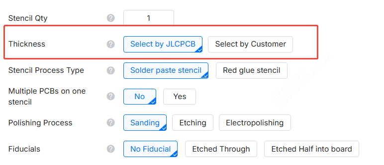
This automated approach reduces human error and ensures better consistency, especially in mixed-component designs.
What Is a Solder Paste Stencil?
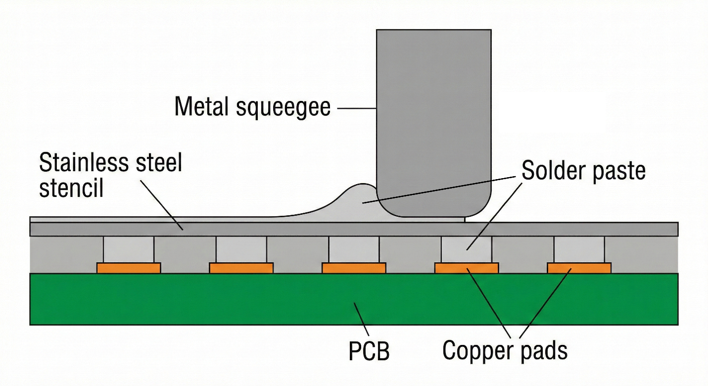
A solder paste stencil is a precision metal sheet used in SMT assembly to control the exact amount of solder paste deposited on PCB pads before component placement.
Most circuit board stencil products are made from stainless steel, typically 304 HTA grade. This material is chosen because it provides high mechanical stability, long-term durability, and resistance to deformation during repeated printing cycles.
The stencil contains precisely aligned laser cut stencil apertures that match the PCB pad layout.
During the printing process:
-
Solder paste is spread across the stencil using a squeegee
-
Paste is forced into the apertures
-
The stencil is lifted, leaving controlled deposits on the PCB
These deposits form the foundation of every solder joint after reflow. Even small variations in stencil quality can lead to inconsistent results.
It is also worth noting that in some assembly workflows, SMD glue stencils are used for wave soldering processes. JLCPCB supports both solder paste and adhesive stencil types depending on manufacturing requirements.
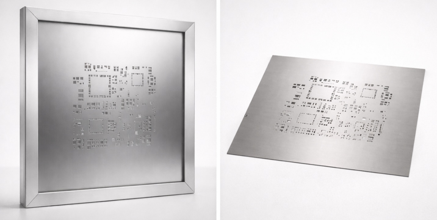
Framed vs Frameless Solder Paste Stencil Options
Choosing between framed and frameless configurations depends mainly on production scale and assembly method.
Frameless PCB Stencil (Foil-Only)
A frameless PCB stencil consists only of the stainless-steel foil without any rigid frame.
It is commonly used because:
-
It is lightweight and easy to handle
-
It has lower cost
-
It works well in manual or semi-manual printing setups
Typical applications include:
-
Prototype assembly
-
Small batch production
-
Laboratory testing environments
Framed Solder Paste Stencil
A framed solder paste stencil is stretched and permanently mounted within an aluminum frame under controlled tension.
This structure provides:
-
Stable and uniform tension
-
Consistent paste release behavior
-
High repeatability across multiple prints
-
Compatibility with automated SMT machines
For production environments where consistency is critical, framed stencils remain the standard choice.
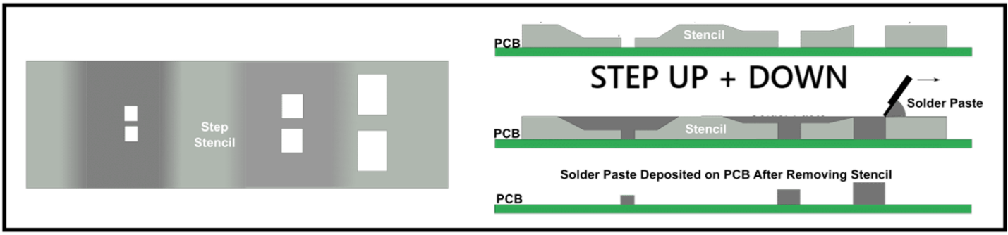
Solving Mixed Layouts with a Step Solder Paste Stencil
Modern PCB designs often include both fine-pitch ICs and large power components on the same board. A single stencil thickness cannot handle both effectively.
A step stencil solves this limitation.
What Is a Step Stencil?
A step stencil is a stencil with localized thickness variations:
-
Step-down areas for fine-pitch components
-
Step-up areas for large pads and connectors
JLCPCB Step Stencil Solution
JLCPCB uses precision milling to adjust stencil thickness in specific regions while keeping the rest of the stencil unchanged.
Benefits
- Accurate solder volume distribution
- Reduced defects during reflow
- Improved yield in mixed-layout designs
For complex boards, a step stencil is often the most practical solution.
Advanced Aperture Rules for Laser Cutting Processes
A laser cut stencil delivers high dimensional accuracy, but final print quality is ultimately determined by how well the aperture geometry is engineered. At this stage, JLCPCB CAM engineers apply strict stencil opening standards to optimize solder paste release, reduce defects, and ensure stable reflow performance across different component types.
1Anti-Solder Beading (Tombstoning Prevention)
For passive components ≥ 0805 (2 × 1.2 mm) or ≥ 5 mm, solder imbalance during reflow can lead to tombstoning or solder bead formation. To prevent paste accumulation and uneven wetting, aperture geometry is modified using optimized shapes such as trapezoidal (home-plate), U-shape, conical, and chamfered U-shape designs. These controlled aperture profiles help balance solder forces on both pads, improving component stability during reflow.
2Bridging Process (Cross-Hatching)
For large thermal pads (≥ 4 × 4 mm), printing a solid solder paste block can trap flux gases, resulting in voiding and weak thermal performance. To address this, JLCPCB applies a window-pane or cross-hatched pattern with a minimum grid spacing of approximately 0.3 mm. This structured pattern allows gases to escape efficiently during reflow while maintaining sufficient solder coverage for thermal and mechanical reliability.
3Via Avoidance (Tenting)
Apertures are carefully designed to avoid overlapping with PCB vias or plated through-holes (PTH) located within pads. This prevents solder paste from wicking down the vias, which would otherwise reduce joint strength and cause inconsistent solder volume distribution across the pad.
4BGA Processing
For BGA assemblies, stencil design supports both reballing and repair workflows. This includes BGA reballing using dedicated fixtures or jigs, as well as pad tinning applications for rework scenarios where no jig is used. Precise aperture control is essential due to the extremely fine pitch and sensitivity of BGA structures.
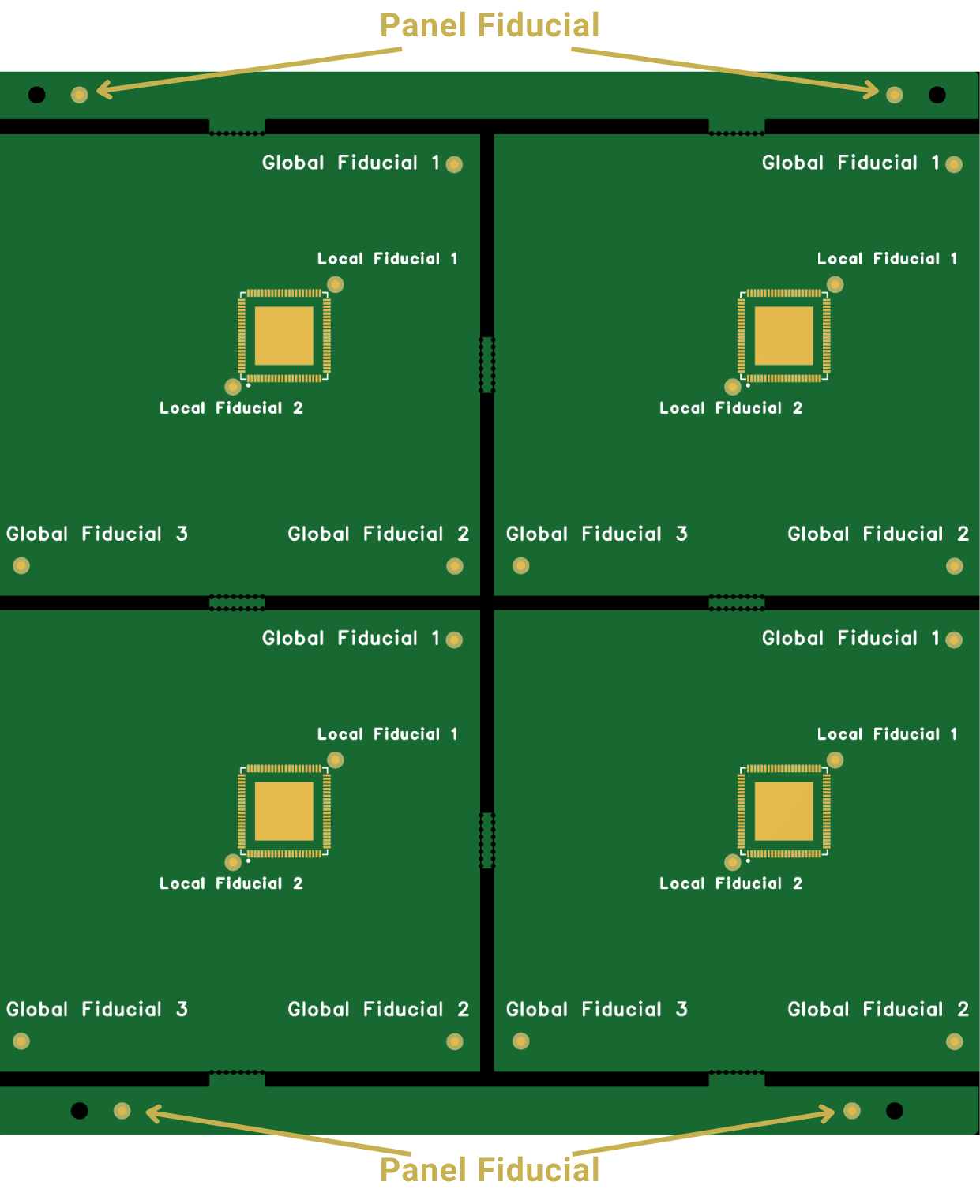
5Fiducial Marks (Alignment References)
Fiducial marks ensure accurate stencil-to-PCB alignment during printing. Options include half-etched marks, which create concave features for automated optical machine vision alignment, and fully pierced marks, which are used for manual alignment processes. In some cases, fiducials may be omitted depending on the PCB assembly strategy and existing board-level references.
Surface Finishes: Electropolishing, Nano-Coating & Electroforming
Surface finish plays a major role in how paste releases from apertures. We focus on advanced industrial treatments:
-
Electropolishing: An electrochemical process that removes microscopic burrs created during laser cutting, producing a smooth mirror-like surface.
-
Electroforming: Utilized for ultra-fine pitch requirements.
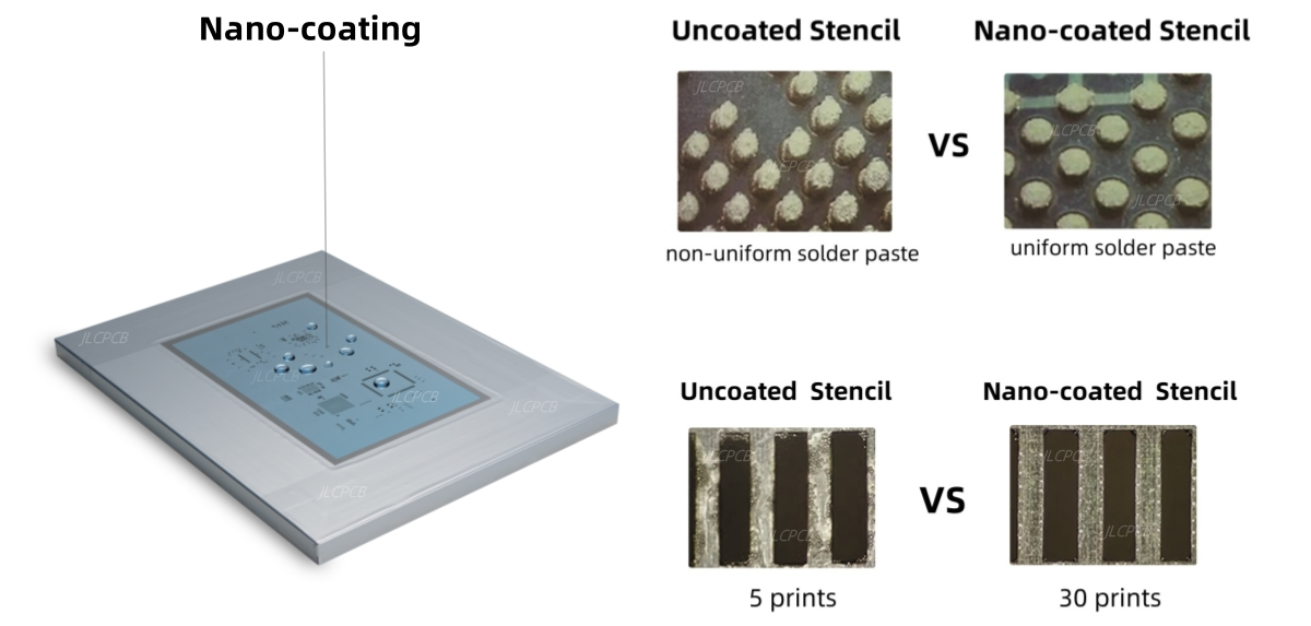
-
Nano-Coating Technology: JLCPCB offers nano-coating using a silicon-fluorine polymer layer applied in a vacuum process.
Benefits
- Increased hardness (400–450 HV)
- Very low surface friction
- Improved solder paste release consistency
- Reduced cleaning frequency
In practical use:
-
Standard stencils may require cleaning every few prints
-
Nano-coated stencils can operate up to 30 prints before cleaning
This improves throughput and reduces downtime in production lines.
Ultrasonic AB Glue Upgrades for Framed Stencils
In high-volume production, stencils must be cleaned frequently to maintain printing quality. Ultrasonic cleaning systems are often used because they are fast and effective.
However, they introduce a hidden issue. The constant vibration combined with chemical exposure gradually weakens the adhesive that bonds the stencil mesh to the aluminum frame.
Standard adhesives (commonly yellow glue) tend to:
-
soften under ultrasonic vibration
-
degrade under heat
-
lose strength when exposed to cleaning solvents
Over time, this leads to mesh separation and stencil failure.
The JLCPCB Solution
JLCPCB solves this issue by using a reinforced bonding system based on ultrasonic-resistant AB glue.
The process includes:
-
Primary bonding using standard adhesive
-
Reinforcement with a secondary layer of imported AB glue
Core Benefits
- Strong mechanical bonding under vibration
- High resistance to temperature changes
- Chemical stability against cleaning agents like IPA
- Long-term structural reliability
This significantly improves stencil durability in continuous production environments.
How to Order Your Custom Solder Paste Stencil From JLCPCB
Ordering a PCB stencil from JLCPCB is designed to be fast, automated, and production-ready from the start. The entire workflow is optimized so you can go from design files to manufacturing in just a few minutes.
Key Features
- Starting price: $3 USD
- No minimum order quantity (MOQ: 1 piece)
- Instant online quotation after upload
Manufacturing Capabilities
-
Precision up to ±0.003 mm
-
High-grade 304 HTA stainless steel
-
Support for Gerber and DXF formats
Available Options
When uploading your files, you can easily configure professional-grade enhancements, including:
-
Step stencil processing
-
Nano-coating for improved paste release
-
Electropolishing for smoother aperture walls
-
Ultrasonic AB glue reinforcement
-
Custom SMT stencil thickness selection
Production can be completed in as fast as 12 hours, with global shipping coverage.
Ready to improve your SMT results? Visit the JLCPCB Stencil Service Page and configure your stencil directly.
Choose from Framed/Frameless, Electropolishing, Nano-coating, Step-Stencils, SMD Glue Stencil and more. Starting at $3. No MOQ. 12-Hour production.
Get $11 Coupon Now >
Frequently Asked Questions about Solder Paste Stencils
When should I use a step stencil?
Use a step stencil when your PCB includes both fine-pitch ICs and large power components requiring different solder volumes.
What is the best SMT stencil thickness for fine-pitch ICs?
For 0.4 mm pitch components, a 0.10 mm SMT stencil thickness is typically recommended.
Does laser cut stencil quality affect solder defects?
Yes, poor aperture precision in a laser cut stencil can directly cause bridging, insufficient solder, or uneven deposits.
Is nano-coating necessary for PCB stencils?
While not required, nano-coating significantly improves paste release and reduces cleaning frequency, especially in high-volume production.
Can one stencil be used for all components?
In simple designs yes, but in mixed-layout boards a step stencil is often required for optimal results.
A properly designed solder paste stencil is a core requirement for stable SMT assembly. It directly controls solder volume, defect rate, and overall production yield.
By selecting the correct >SMT stencil thickness, applying step stencil techniques for mixed layouts, optimizing laser cut stencil aperture design, and using advanced surface treatments like nano-coating and AB glue reinforcement, engineers can significantly improve manufacturing consistency.
JLCPCB enables these capabilities in a cost-effective and accessible way, making professional-grade PCB stencil production available for both prototyping and large-scale manufacturing.
Keep Learning
How to Choose a Solder Paste Stencil (Thickness, Step Stencil & Design Guide)
In SMT assembly, the stencil quietly decides whether a production run succeeds or fails. Problems like bridging, tombstoning, and insufficient wetting are frequently traced back not to PCB design errors, but to incorrect stencil selection or poorly controlled paste volume. Quick Answer: How to Choose a Solder Paste Stencil If you need to define your stencil parameters immediately, follow this quick decision guide: Select thickness based on component pitch: Use component density as your primary baselin......
Custom Cut Stencils for PCB Assembly: How to Cut, Use and Choose the Right PCB Stencil
Custom-cut stencil and Solder paste printing are two of the most vital processes in Surface Mount Technology (SMT) PCB assembly, concerning solder joint quality, electrical performance, and product reliability over time. SMT stencils are used to deposit solder paste in accurate amounts onto PCB pads, or for depositing and compressing adhesive pastes which are arranged in the form of a column on components such as connectors and sockets. While PCB designs have seen a trend toward increased density, fin......
Custom Stencil Maker: How Custom SMT Stencils Are Designed, Made, and Used
Custom stencils and solder paste printing are two of the most critical processes in Surface Mount Technology (SMT) Assembly, which directly affect the quality, reliability, and performance of electronic products. Before a component is placed on it, the SMT stencil is responsible for controlling how much and where solder paste is applied onto PCB pads. A well-defined stencil leads to less variation in joint geometry and size, as well as producing better production yield. To reach that level of accuracy......
Choosing the Right Stencil Maker for PCB Assembly
Surface mount technology assembly relies on controlled solder paste deposition across dense PCB pad layouts. SMT stencil makers regulate paste volume through apertures that match copper land patterns. A stencil maker machine influences solder joint geometry, electrical continuity, and reflow consistency. Laser cut stencil maker systems achieve aperture accuracy and stencil flatness for automated printing. Stencil makers exist as local stencil maker near me services and scalable online stencil maker pl......
Understanding SMT Stencil Printers for Accurate PCB Solder Paste Printing
Stencil printing is a critical process in SMT (Surface Mount Technology) assembly, significantly impacting the quality and reliability of solder joints on PCBs. The crucial machine for implementing this is the SMT Stencil Printer, which applies an appropriate measure of solder paste to each pad of the PCB board before it goes to the placement of components. For those of you looking to work out what a stencil printer is and why it matters in manufacturing, you've come to the right place. This is the ba......
Stencil Cutting Machine Guide: Choosing the Best Solution for PCB Stencil Manufacturing
In the PCB assembly process using Surface-Mount Technology (SMT), precision plays a critical role in determining the final quality of a market-ready product. One of the most crucial stages in SMT is the solder paste printing process, which is the first step in the SMT production line. In this process, the stencil functions as the medium that distributes solder paste onto each component pad. At this stage, the stencil cutting machine plays a vital role in determining the overall success of the assembly......