Solder Paste Printing Defects: How Precision Stencils Prevent Assembly Failures
12 min
- Common Solder Paste Printing Defects and Their Impact
- Root Causes: Why Do Solder Paste Printing Defects Occur?
- How Stencil Engineering Impacts Solder Paste Printing Yield
- Utilizing Solder Paste Inspection (SPI) to Quantify Defects
- Why Choose JLCPCB Precision Stencils for High FPY?
- FAQ about Solder Paste Printing Defects
Key Takeaways
70% Rule: Approximately 70% of SMT defects originate from the solder paste printing stage, making it the most critical process to optimize.
Root Causes: Defects like bridging, insufficient paste, misalignment, and slumping are caused by stencil tension, process parameters (pressure, speed), and paste chemistry/environment.
Area Ratio Matters: Maintaining an aperture Area Ratio (AR) above 0.66 (per IPC-7525) is essential to ensure proper paste transfer efficiency and prevent chronic insufficient deposits.
SPI is Key: Automated Solder Paste Inspection measures height, coverage, and volume to catch defects before reflow, enabling data-driven process control.
Stencil Quality: High-quality stencils with electropolishing, nano-coating, and 304 HTA stainless steel are the most cost-effective intervention to achieve high First Pass Yield.
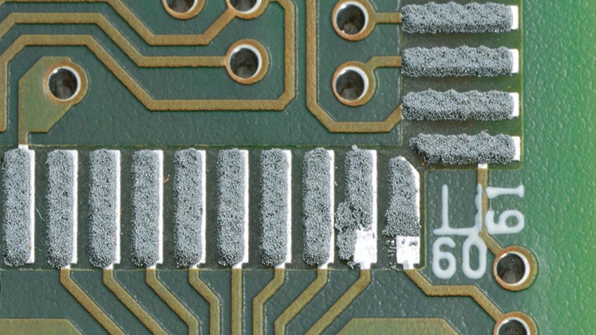
The 70% Rule has been proven in industry practice: approximately 70% of SMT defects arise from the printer. If you do choose the placement and reflow option, a bad deposit will not be corrected. The smaller the components, the less leeway for error. The quicker the process of printing is mastered, the greater the yield will be attained, and the greater the rework costs will be reduced.
Mechanical and environmental influences that affect solder behavior, such as stencil tension and ambient humidity, are discussed in this guide. You'll understand the concepts behind precision tooling and its ability to take the printing process from variables to repeatability.
Common Solder Paste Printing Defects and Their Impact
A good solder paste deposit can be used to predict the reliability of a solder joint. There are different downstream risks associated with each defect type.
Solder Bridging and Smearing
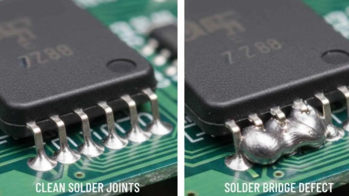
Solder bridging (extraneous solder between the two components) is a short. The small conductor gap is a very important problem in fine pitch packages (QFNs and micro-BGAs).
There's a precursor to that, and that is smearing when the gasket seal fails, the paste will bleed through, and this will lead to solder satellites on the next board, or solder residue on the solder mask.
See JLCPCB's guide on Preventing Solder Bridging for more information on corrective strategies.
Insufficient Solder Paste
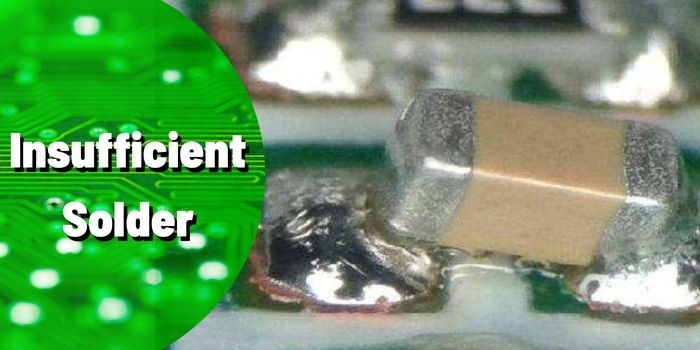
Open joints can occur, as can solder joints that pass electrical tests and fail during thermal and/or vibration stresses, a very bad scenario for a BGA device, as the solder joint is the only mechanical and electrical connection.
The 5-Ball Rule (IPC-7525)
The smallest aperture dimension should be at least 5 times the diameter of the largest solder powder particle. For Type 4 paste with particles up to 38 µm, that means a minimum aperture of about 0.19 mm; for Type 5 (particles up to 25 µm), about 0.125 mm. Below this ratio, surface tension holds the paste inside the aperture instead of releasing it cleanly onto the pad, causing insufficient deposits on fine-pitch components.
Offset and Misalignment
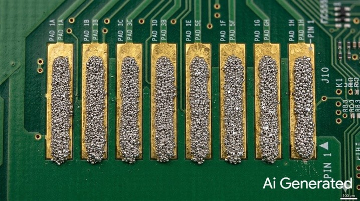
If it is not formed correctly and separated from the PCB pad, it is called Misregistration. If the pad offset exceeds 20% of the Pad width, it is considered as a quality requirement for fine pitch components and is normally a guideline requirement for process control.
The differential surface tension of a two-terminal component during the reflow process, after one of the pads is wet first, is the most common cause of tombstoning.
Slumping and Peak Scavenging
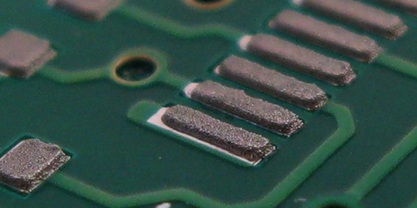
If the paste does slump to the sides after separating the stencil, it is considered "slump" and, as a consequence, will decrease the separation between the pads and will cause bridging during reflow. The flux has high viscosity in the cold (room-temperature) state and low viscosity in the hot (reflow-oven) state.
A separate cause of low paste volume is "scooping" (also called scavenging), where a too-soft squeegee or excessive blade pressure digs into large apertures and removes paste instead of wiping cleanly across the stencil surface. The result is a concave deposit with reduced height in the middle, which produces insufficient solder volume on power components and large pads. Switching to a harder (metal) squeegee or reducing blade pressure usually corrects it.
| Defect | Visual Characteristic | Downstream Risk |
|---|---|---|
| Solder Bridging | Connection between conductors | Electrical short, component failure |
| Insufficient Paste | Missing or thin deposit | Open circuit, weak joints |
| Misalignment | Deposit off-center | Tombstoning, poor wetting |
| Smearing | Residue outside the pad area | Solder balls, random shorts |
| Scooping | Concave paste surface | Inadequate joint volume |
| Slump | Spread of paste edges | Bridging during reflow |
Choose from Framed/Frameless, Electropolishing, Nano-coating, Step-Stencils, SMD Glue Stencil and more. Starting at $3. No MOQ. 12-Hour production.
Get $11 Coupon Now >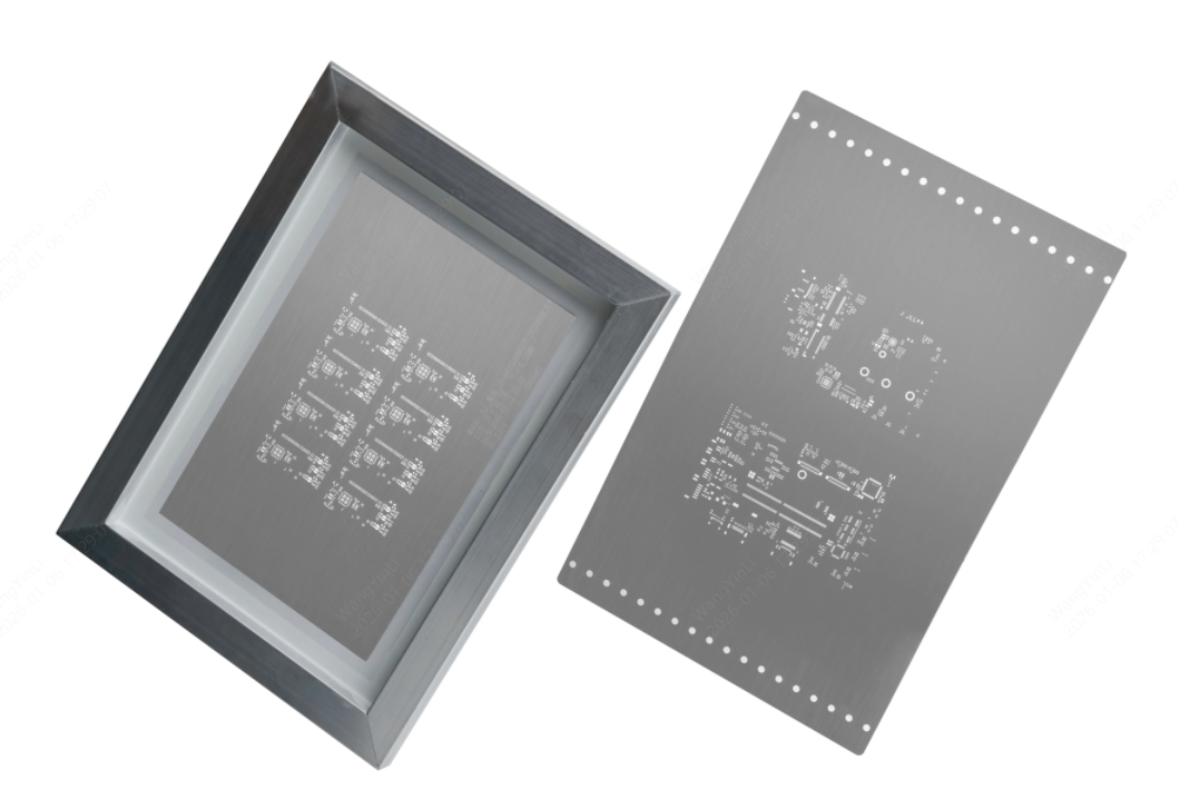
Root Causes: Why Do Solder Paste Printing Defects Occur?
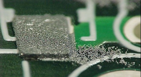
The printer hardware, stencil engineering, paste material science and surrounding environment must be taken into account as tools that can be used to either drive the process further out of or further into control in a comprehensive diagnostic analysis.
The Stencil Variable: Tension and Geometry
If the tension of the foil is not high enough during the squeegee stroke, the gasket seal is damaged, and smearing is applied.
The ratio of the volume of the deposited paste to the theoretical aperture volume is termed Transfer Efficiency (TE) and is a function of the ratio of the volume of the aperture-opening to the surface of the aperture-walls called Area Ratio (AR).
Area Ratio Minimum (IPC-7525)
The industry minimum AR value is 0.66 (per IPC-7525). Below this threshold, the paste's adhesion to the aperture walls becomes greater than its adhesion to the PCB pad, so the paste stays inside the aperture rather than releasing onto the pad during stencil lift-off. This is the dominant cause of insufficient paste deposits on fine-pitch components, and the reason area ratio is one of the first things to check when chasing chronic skip or low-volume defects.
Process Parameters: Pressure, Speed, and Separation
- Squeegee Pressure: Typically 0.3–0.5 N/mm of squeegee length, with lower pressure preferred for finer-pitch components. Excessive pressure causes "scooping," where the blade forces paste out of large apertures instead of transferring it cleanly to the pads.
- Squeegee Speed: 25–50 mm/s. Slower speeds (closer to 25 mm/s) help fine-pitch apertures fill completely; faster speeds (closer to 50 mm/s) work for larger components and higher throughput, but risk insufficient fills on narrow apertures.
- Separation Speed: 0.1–3 mm/s for fine pitch work. High speeds result in tall, thin paste peaks that slump and/or interfere with each other.
Solder Paste Chemistry and Environment
Solder paste is thixotropic, meaning that it thins down when stressed and then reforms into a paste when it is not stressed. The temperature should be at 22°C–26°C; if it is too high, it will become thinner, and a slump will occur. Humidity must be held at 45% ± 5%.
When excess humidity exists, there is an increased flux absorbency, and solder balling occurs during reflow. Because condensation can cause a chemical imbalance, paste that is taken out of the refrigerator must be conditioned for 2–4 hours at room temperature before opening the container.
While several factors contribute to solder paste printing yield, it's fundamentally limited by stencil quality.
How Stencil Engineering Impacts Solder Paste Printing Yield
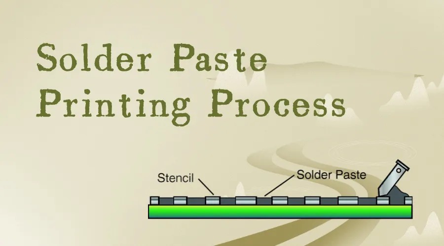
Printer parameters can be set. If the stencil is not well-engineered, you will produce defects on the machine.
Stencil quality is the ultimate ceiling for printing yield, making professional tooling the most cost-effective way to prevent SMT soldering defects.
304 HTA Stainless Steel and Foil Tension
The 304 HTA (Tension Annealed) Stainless Steel is used in high-quality stencils and is designed for use in high-stress applications that demand a high level of flatness and internal tension over thousands of print cycles.
This material will not cause stencil sag to ensure a uniform gasket seal with the PCB and eliminate solder paste printing issues like misregistration and smearing.
Aperture Geometry and Opening Process Standards
The aperture accuracy is ±0.003 mm by laser cutting, and the aperture is adjusted to suit the size of the pad. Aperture process standards usually decrease the size of large pads by 10–20% to avoid excess volume, or increase the size of small pads to ensure the appropriate deposition amount.
Adhering to a strict Opening Process Standard is mandatory to prevent insufficient solder paste on fine-pitch components.
Surface Finish
Surface finish of the stencil also has a huge effect on the solder paste printing process.
Electropolishing
A process that clears tiny burrs from the walls of the apertures using an electrochemical process. These walls can be smoothed to reduce friction and provide almost 100% of paste release.
Nano-Coating
The bottom of the stencil and the wall of the aperture are treated with a hydrophobic/oleophobic coating. It resists flux and solder particles, which helps to reduce the wicking under the stencil and extends under stencil cleaning time from 1–3 prints to 20–50 prints, which is a huge throughput improvement for high-volume production.
Utilizing Solder Paste Inspection (SPI) to Quantify Defects
"You can't manage what you don't measure." Automated SPI is the metrological connection between the printing process health and measurable and actionable data.
SPI machines measure each deposit of paste across three key metrics:
- Height (Z-axis): Can detect scooping or excessive thickness of the paste deposit.
- Bridging and/or pad coverage (X-Y footprint) detection.
- Volume: The most critical measurement, based on height and area data, to ensure sufficient solder mass for joint formation.
The strength of the diagnostic power of SPI is that it can "read" the trends. If the volume is trending downwards on several boards, it suggests a worn squeegee or a gradually clogging stencil. A sudden uniform X-Y offset across all pad points indicates mechanical misalignment in the board clamping or vision system.
By catching solder paste inspection defects before boards enter the reflow oven, SPI eliminates the significantly greater cost of post-reflow rework.
For implementation guidance, see JLCPCB's comprehensive Solder Paste Inspection (SPI) Guide.
Why Choose JLCPCB Precision Stencils for High FPY?
For both rapid prototyping and mass production, the quality of the stencil provider is the primary determinant of printing yield. JLCPCB offers professional-grade stencils engineered to address all the variables discussed in this guide.
Technical Specifications
- Laser Precision: ±0.003 mm tolerance ensures apertures' exactness to design specifications.
- Material: 304 HTA stainless steel to maintain foil tension and gasket seal.
- Thickness: 0.06 mm to 0.3 mm for ultra-fine-pitch components or high-power electronics, respectively — the vast majority of industry standards.
- Processes: Nano-coating, electropolishing, step stencils, and ultrasonically resistant adhesives for complex multi-component boards.
Logistical Advantages
- Build Time: Industry-leading, as fast as a 12-hour turnaround.
- Pricing: Starting at $3 USD with no minimum order quantity.
- Global Shipping: 180+ countries.
- Ordering: Upload Gerber or DXF files, get a quote in as little as 5 minutes.
FAQ about Solder Paste Printing Defects
Q: What are the differences between framed and frameless stencils?
Framed stencils are mounted in a rigid aluminum frame for the best stability and repeatability for automatic SMT lines. Frameless stencils (foils) are used in conjunction with a tensioning system, are ideal for prototyping, cost-effective, and easy to store, but can be easily damaged, and if not handled properly, may not align correctly during printing.
Q: What kind of solder powder do you use for printing?
Particle size must match the smallest aperture on your stencil. The 5-ball rule (per IPC-7525) states that the smallest aperture should be at least 5 times the diameter of the largest powder particle. For most modern SMT work down to 0.5 mm pitch, Type 4 paste (particles up to 38 µm) is the default. For 0201, 01005, and 0.4 mm pitch BGA work, step down to Type 5 (particles up to 25 µm) so the paste releases cleanly from very small apertures. Over-sized particles may block the holes and lead to insufficient paste deposits.
Q: When is a step stencil required?
A step stencil is a stencil with multiple foil thicknesses. This is needed when different components on a board need different volumes of solder paste printed; for instance, a fine-pitched Ball Grid Array (BGA) component requires 0.1 mm of paste, but a large power connector requires 0.15 mm of paste to give it adequate support.
Q: How frequently should you clean the under-stencil?
Standard practice without surface treatments is every 1–3 prints for fine-pitch work. Stencils with nano-coating extend this interval to every 20–50 prints. Cleaning frequency should also increase if SPI data show a progressive downward trend in paste volume, indicating paste accumulation on the underside of the stencil.
Conclusion: Preventing SMT Defects with Precision Stencils
Solder paste defects are not inevitable. By using the 70% Rule as a guide and optimizing stencil engineering, companies can significantly raise their First Pass Yield.
Success requires balancing variables like stencil tension and humidity. Investing in precision tooling remains the most cost-effective intervention. It transforms a volatile stage into a stable, repeatable operation.
Keep Learning
Low-Temperature Solder Paste: A Practical Sn-Bi Guide
Key Takeaways Sn42Bi58 is the mainstream low-temp alloy and melts at 138 C. Typical reflow peak is 165 to 180 C, about 25 to 30 C above the melt. It protects heat-sensitive components and reduces warpage on large, thin boards. It enables step soldering, because 165 to 180 C will not remelt SAC305 joints. Bismuth joints are more brittle than SAC305, so avoid drop-critical products. Never mix Sn-Bi with leaded (Sn-Pb) solder. Bi, Sn and Pb form a ternary eutectic that melts near 95 C. Some parts and som......
Pin-in-Paste: Through-Hole Reflow With a Stencil
Key Takeaways One Reflow Process: Pin-in-paste combines SMT and through-hole soldering into a single reflow pass, eliminating the need for separate wave, selective, or hand-soldering steps when the board has only a few through-hole components. Paste Volume Is Critical: Solder paste is roughly 50% flux by volume, so you need to print about twice the solder volume the finished joint requires. Stencil design—overprint apertures and step-up zones—makes or breaks the process. Target 75% Barrel Fill: Per IP......
Mixed Technology PCB Assembly: Combining SMT and THT on One Board
As technologies become increasingly more complex, the demand for sophisticated printed circuit boards continues to rise. In the electronics industry, the two most prevalent PCB Assembly technologies are SMT and THT, which differ mainly in the manner at which the components are attached. SMT places the components on the surface of the board whereas THT makes use of drilled holes to solder components. While these technologies individually cater to specific applications, advancements in the electronics i......
Moisture Sensitivity Level (MSL): Baking Guide
Key Takeaways Moisture Sensitivity Level (MSL) is a 1-6 classification under IPC/JEDEC J-STD-020 that indicates how quickly a non-hermetic surface-mount package can absorb enough moisture to become vulnerable during reflow. MSL 1 has unlimited floor life at its reference condition, while MSL 6 requires baking before use and reflow within the time printed on the caution label. The floor-life clock begins when the moisture barrier bag is opened and exposure to factory air starts. Baking according to IPC......
Understanding SMT Stencil Printers for Accurate PCB Solder Paste Printing
Stencil printing is a critical process in SMT (Surface Mount Technology) assembly, significantly impacting the quality and reliability of solder joints on PCBs. The crucial machine for implementing this is the SMT Stencil Printer, which applies an appropriate measure of solder paste to each pad of the PCB board before it goes to the placement of components. For those of you looking to work out what a stencil printer is and why it matters in manufacturing, you've come to the right place. This is the ba......
Surface Mount Stencil: A Practical Guide for SMT Printing and Solder Paste Application
It starts with a slim piece of metal, slipped in early during assembly. Before any part lands in place, before heat ever touches the board, that layer shapes the flow. Where the paste spreads comes down to its design. How thick it is, how it's cut - those details decide what sticks and what washes away. For engineers looking for reliable stencils, JLCPCB provides high-precision SMT stencils that integrate seamlessly with PCB production workflows. Down goes solder paste, slipping through narrow cuts in......