
Stencil in PCB: A Comprehensive Guide to PCB Stencil Design, Fabrication, and JLCPCB Solutions
6 min
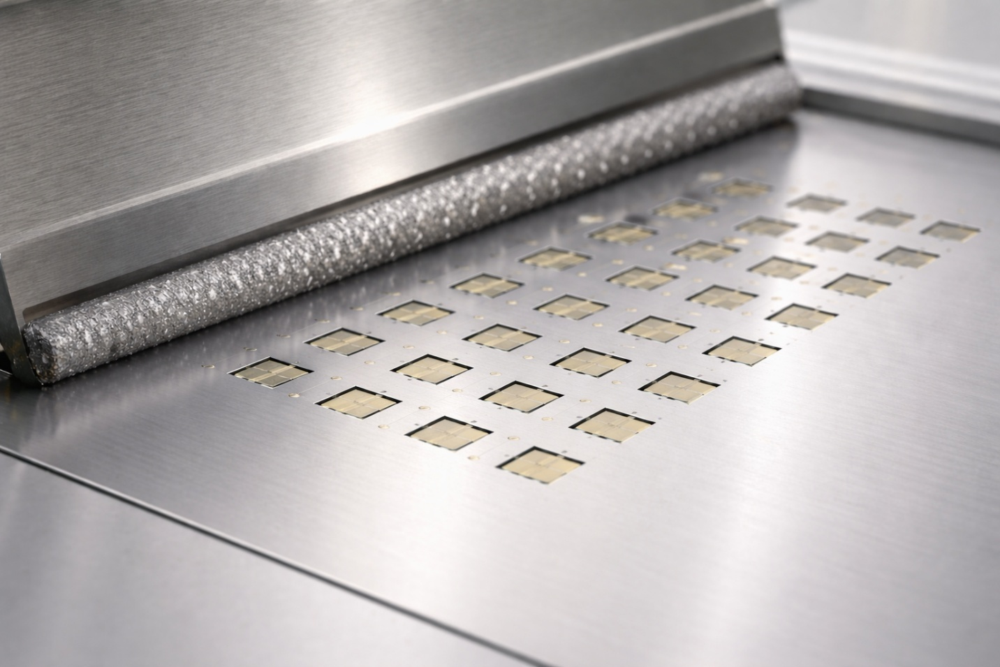
Figures 1 Solder paste application using a stainless steel stencil to achieve high-precision results.
In PCB assembly based on Surface-Mount Technology (SMT), precision is a key factor that determines the final quality of electronic products. One critical element that strongly influences soldering accuracy is the stencil. The stencil functions as a physical template that controls the distribution of solder paste onto PCB pads before components are placed.
Accurate solder paste application produces reliable solder joints, reduces defects such as solder bridging or insufficient solder, and improves overall SMT process reliability. Whether in prototyping or production stages, proper stencil design and fabrication methods play an important role in maintaining consistent assembly results.
This article discusses the role of stencils in PCB assembly, covering their applications, design and fabrication principles, and practical solutions ranging from DIY approaches to JLCPCB stencil services.
Understanding Stencils in PCB
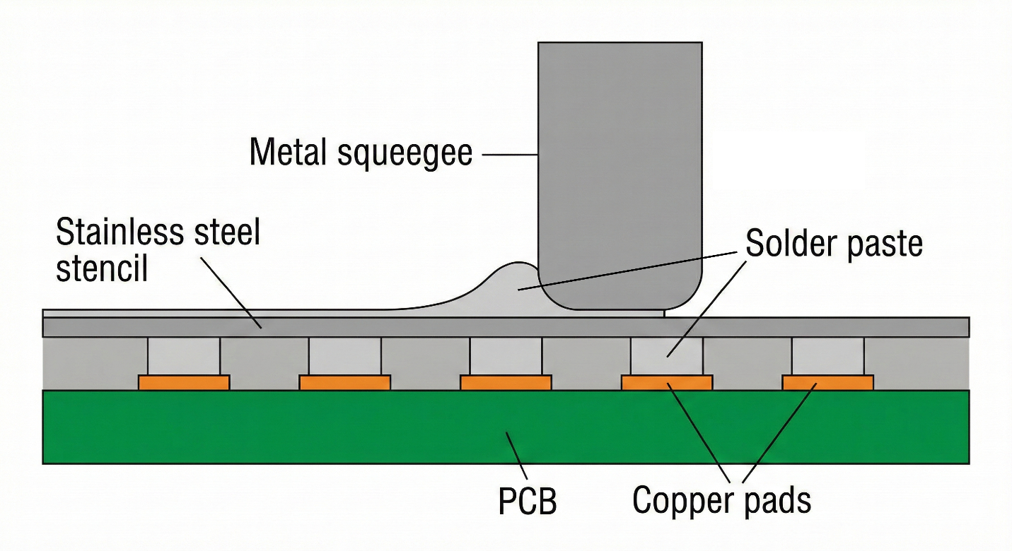
Figures 2 Illustration of how a stencil limits solder paste deposition to PCB pad areas.
What Is Stencil in PCB?
In the PCBA process, a stencil is a thin sheet—typically made of stainless steel—with apertures that match the solder pad layout of the PCB design. During solder paste printing, the stencil is aligned over the PCB so that solder paste is deposited only on the intended pad areas.
In SMT production, the stencil is usually used at the early stage of the manufacturing line. As a result, stencil quality has a significant impact on subsequent processes such as component placement (Pick and Place Machine) and reflow soldering. Poor stencil design or fabrication can lead to repeated defects throughout the assembly process.
Key Functions and Benefits
The primary function of a PCB stencil is to control the volume and position of solder paste. Key benefits of using a properly designed stencil include:
· Consistent solder paste distribution on each pad
· Reduced solder defects such as bridging and tombstoning
· Good repeatability for batch and mass production
· Higher production yield and lower rework rates
Proper use of stencils in PCB assembly helps create stable solder joints and improves the long-term reliability of electronic products.
Fabrication and Design Principles
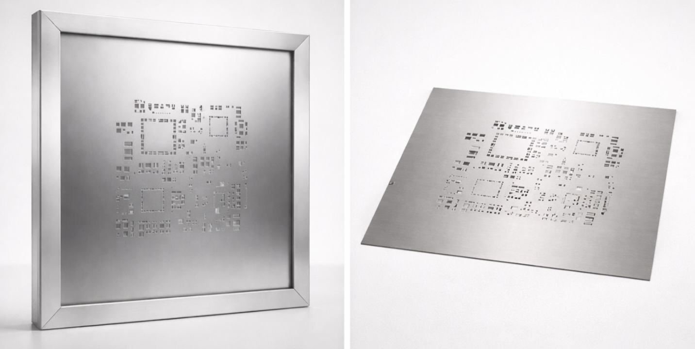
Figures 3 Comparison between framed stencils for automated production (left) and frameless stencils for manual prototyping (right).
Materials and Thickness Selection
Material selection is an important factor in PCB stencil design. Stainless steel is the most commonly used material due to its high durability, smooth surface finish, and suitability for laser cutting processes.
Stencil thickness determines the amount of solder paste transferred to PCB pads. Common thickness ranges from 0.08 mm to 0.15 mm, depending on component type and size. Thicker stencils deposit more solder paste, while thinner stencils are preferred for fine-pitch components to reduce the risk of solder bridging.
Professional services such as JLCPCB stencil solutions offer multiple thickness options to accommodate different PCB design requirements.
Aperture Design and Layout
Aperture design significantly affects solder paste release during the printing process. In many cases, aperture size is intentionally reduced rather than matching the PCB pad size exactly, in order to control solder volume.
Key considerations in aperture design include:
· Aperture shape (square, rounded, or specially modified geometries)
· Area ratio and aspect ratio to ensure proper solder paste release
· Spacing between apertures in dense pad layouts
Proper aperture design is a critical aspect of PCB stencil design, particularly for fine-pitch ICs, QFN packages, and BGAs.
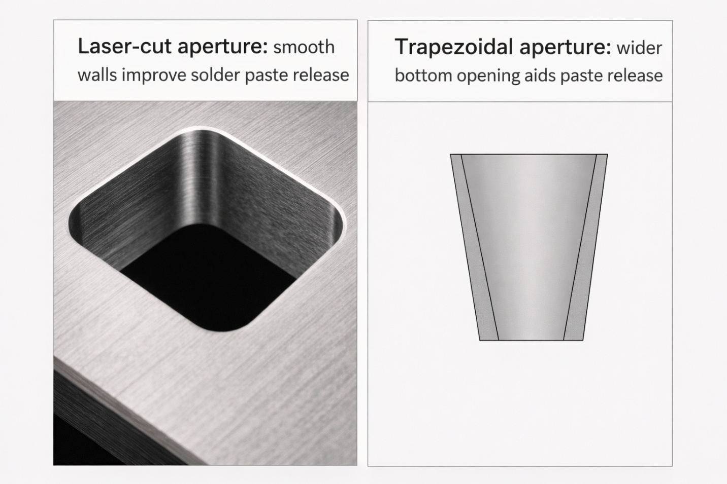
Figures 4 Trapezoidal aperture shapes and smooth laser-cut walls ensure optimal solder paste release.
Manufacturing Methods
Several manufacturing methods are used to produce stencils for PCB assembly:
· Laser cutting – The industry standard, offering high precision and smooth aperture edges
· Chemical etching – Lower cost but reduced accuracy and edge quality
· Mechanical cutting – Rarely used due to low precision
Laser cutting is widely preferred for professional applications, especially for high-density SMT designs.
DIY and JLCPCB Stencil Solutions
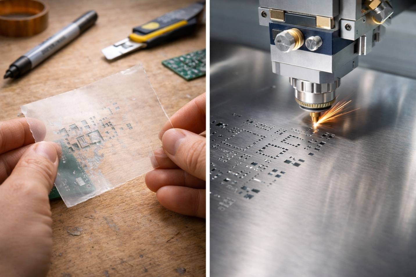
Figures 5 Comparison between manual DIY stencil fabrication and industrial laser cutting methods.
DIY Stencil Techniques
For hobbyists or early-stage prototyping, DIY PCB stencil approaches are still commonly used. Typical DIY methods include plotters, vinyl cutters, or low-cost manual stencils.
While suitable for simple designs, DIY stencils have limitations in terms of precision, aperture consistency, and material durability. The risk of solder defects is generally higher, especially for PCBs with fine-pitch components or high-density layouts. Therefore, DIY approaches are best suited for learning purposes, early experimentation, or low-complexity PCB designs.
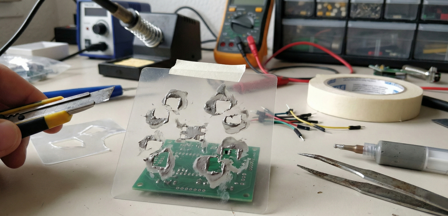
Figures 6 Manual stencil fabrication using polyimide materials often has limited precision for fine-pitch components.
In addition to technical limitations, health and safety considerations should also be taken into account when using DIY stencils. Manual cutting processes, cleaning chemicals, and exposure to solder paste may introduce risks such as minor hand injuries, skin irritation, or exposure to fine particles if proper procedures are not followed.
Uncontrolled aperture quality in DIY stencils can also increase the need for rework, which indirectly raises exposure to heat and chemicals during assembly. Therefore, basic protective equipment and a suitable working environment are strongly recommended, especially when performing repeated solder paste printing.
For more complex applications or repeated production, many engineers choose professional stencil solutions to minimize operational risks while improving consistency and assembly reliability.
JLCPCB Stencil Services
For professional and production-ready requirements, JLCPCB stencil services provide a more reliable solution. Using industrial-grade laser cutting technology, JLCPCB produces stencils with consistent aperture quality and high precision based on PCB design files.
Key advantages of JLCPCB stencil services include:
· A wide range of stencil thickness options
· Support for high-density PCB layouts
· Consistent quality across production batches
· Integration with PCB manufacturing and assembly services
Optional features such as electropolishing provide smoother aperture walls to improve solder paste release efficiency, while nano-coating options help reduce stencil cleaning frequency.
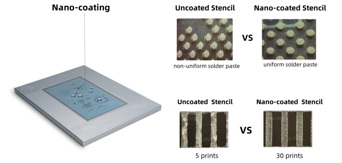
Figures 7 JLCPCB stencil with laser-cut technology and optional nano-coating for high durability and consistent printing results.
These solutions are suitable for both advanced prototyping stages and mass production.
Best Practices for PCB Stencil Use
Solder Paste Printing Tips
To achieve optimal solder paste printing results, several best practices should be followed:
· Ensure accurate stencil-to-PCB alignment
· Use appropriate squeegee pressure and angle
· Select solder paste compatible with stencil thickness
· Perform regular inspection of printed solder paste
Consistent printing parameters help maintain stable SMT process performance.
Maintenance and Cleaning
Proper stencil maintenance extends stencil lifespan and ensures consistent solder paste transfer. Regular cleaning removes solder paste residue from apertures, preventing clogging and printing defects.
Cleaning methods include:
· Manual wiping with lint-free materials
· Solvent-based cleaning
· Automated stencil cleaning systems
Routine maintenance is essential for sustaining assembly quality, especially in repeated production cycles.
Conclusion
Stencils in PCB assembly are fundamental elements that directly influence soldering quality, process stability, and manufacturing efficiency. Proper stencil design, appropriate material selection, and reliable fabrication methods enable accurate and consistent solder paste application.
By applying best practices in printing, maintenance, and service selection, engineers can significantly improve SMT process performance. Whether using DIY PCB stencils for simple prototypes or relying on JLCPCB stencil solutions for high-precision applications, selecting the right approach has a direct impact on product quality and overall production efficiency.

Keep Learning
SMT Stencil Cleaning Guide: Process, Frequency, and Tips
Key Takeaways about SMT Stencil Cleaning SMT stencil cleaning removes solder paste residue from aperture walls and the stencil underside, keeping paste transfer efficiency between 80% and 100%. Industry analysis attributes over 60% of SMT defects to the paste-print step — most of which trace back to a stencil cleaning lapse. Two stages matter: under-screen cleaning (between cycles, typically every 5–10 prints) and off-line cleaning (after production completes). IPA handles standard flux residue; dedic......
Top 5 Circuit Board Stencil Mistakes & How to Fix Them for Higher SMT Yield
Usually, the circuit board stencil is responsible for roughly 60% to 70% of all SMT defects. That number surprises people. It shouldn't. The stencil controls paste volume, deposit geometry, and positional accuracy all at once. When it gets wrong, everything downstream pays for it. The shift in thinking that separates good engineers from great ones is simple: stop seeing the PCB stencil as a metal sheet with holes in it. It is a precision fluid delivery system. Every aperture wall, every micron of foil......
How to Apply SMD Glue Using SMT Stencils (Design, Thickness & Troubleshooting Guide)
The reality of modern PCB assembly is that "mixed-technology" is still very much the norm. When a board hits the wave soldering machine, bottom-side SMD components face a high-velocity river of molten metal. Without a solid mechanical bond, they’ll simply wash away into the solder pot. That’s where the precision application of SMD glue becomes the difference between a successful run and a bin full of scrap. Quick Answer: How to Apply SMD Glue in SMT If you need to configure your SMT stencil for adhesi......
The Essential Guide to SMT Stencils in PCB Assembly
Introduction In the dynamic world of electronics manufacturing, Surface Mount Technology (SMT) plays a crucial role in achieving efficiency and precision in printed circuit board (PCB) assembly. Central to the SMT process is the SMT stencil, an indispensable tool for the accurate application of solder paste. This ensures solid electrical connections between components and PCBs. This guide delves into the specifics of SMT stencils, examining their types, materials, manufacturing methods, advantages, ch......
Nano-Coatings in PCB Manufacturing: How They Outperform Traditional Stencils
Nano coating is a thin hydrophobic (water repellent) and oleophobic (oil repellent) treatment used on the undersides and edges of solder paste stencils. With this the surface becomes non-stick which reduces the number of cleaning cycles required for the solder paste printing process. Upon application, the less than 5 nanometer coating bonds with the stencil foil at the microscopic level, which does not change the size and shape of the stencil. Nano coating is an industry proven process which shows imm......
How to Choose an SMT Stencil
What is an SMT stencil? SMT Stencil is a thin metal sheet used in the soldering process for SMT (Surface Mount Technology) and it plays an essential role in the SMT soldering process. Smt Stencil allows the direct placement of solder paste onto the SMD pads of PCB, which can help prevent errors and defects during the reflow soldering process. This results in a precise amount of tin coverage once the work is completed. Types of SMT Stencils Depending on the application of solder paste, there are three ......