
Solder Bridging: Preventing a Common PCB Soldering Defect
8 min
- What is Solder Bridging?
- What Causes Solder Bridging in PCB Assembly?
- How SMT Stencil Design Acts as the First Line of Defense?
- Practical Strategies to Eliminate Bridging During Production
- Why JLCPCB Stencils Are the Best Choice for Short-Free Assembly?
- Conclusion: Achieving Perfect Yield With the Right Tools
- How can solder bridging be prevented during reflow soldering?
- How do you detect a PCB solder bridge?
- Can a solder bridge be repaired?
- Why do fine-pitch components increase the risk of solder bridging?
- Does stencil thickness affect solder bridging?
- Is solder bridging a common SMT soldering defect?
Modern electronics demand compact PCB layouts with dense pad spacing and miniature components. Engineers deploy 0201 packages, fine pitch QFN devices, and large BGA arrays across SMT assembly lines. These layout conditions increase complexity during reflow soldering and raise the probability of PCB soldering defects. Solder bridging appears frequently within high-density boards that contain narrow pad spacing and large solder paste deposits.
A solder bridge forms an unintended conductive path between adjacent pads or copper traces. This solder bridging defect produces electrical shorts that interrupt circuit function and reduce production yield. Engineers control solder paste deposition through precise PCB stencil design. High precision stencil fabrication services, such as JLCPCB stencils, improve solder paste release and reduce solder bridging risk in dense SMT assembly layouts.
What is Solder Bridging?
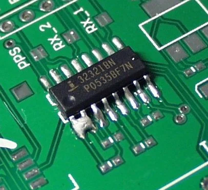
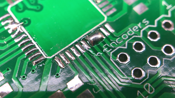
Solder bridging is an unintended electrical connection between two or more adjacent pads, pins, or PCB traces. This PCB soldering defect occurs when excess solder, misaligned components, or improper stencil application cause molten solder to join neighboring conductors. The resulting short circuit can disrupt electrical continuity, damage components, or cause complete board failure.
IPC-A-610 standards classify solder bridging as an unacceptable solder joint condition. Assemblies with bridges fail inspection because proper electrical isolation between pads and leads is mandatory. Visible bridges often appear on QFP packages, fine-pitch ICs, or connectors, where solder flows across adjacent pins.
Hidden solder bridges occur under BGA components, where solder balls join unseen, increasing the risk of latent failures. Detection of hidden bridges requires X-ray inspection, while visible bridges can be identified with optical inspection or magnification. Controlling solder paste volume, maintaining stencil alignment, and ensuring precise component placement reduce both visible and hidden solder bridging defects in high-density SMT assemblies.
What Causes Solder Bridging in PCB Assembly?
Solder bridging arises from multiple technical factors during SMT assembly. Understanding the root causes allows engineers to prevent defects and improve PCB yield. The most common sources relate to solder paste application, component placement, stencil condition, and reflow parameters. Each factor influences how molten solder behaves on fine-pitch pads and dense PCB layouts.
The key causes of solder bridging in PCB assembly are listed below:
1. Excessive Paste Volume: Applying too much solder paste increases the risk of “slump” during reflow. The surplus molten solder flows across neighboring pads, forming unwanted connections. Correct stencil thickness and paste volume control mitigate this issue.
2. Poor Component Alignment: Misplaced or off-center components push solder into adjacent gaps. Fine-pitch ICs and connectors are highly sensitive, making precise placement essential to avoid bridging.
3. Stencil Smearing: Residue on the underside of the PCB stencil leaves trails of paste between pads. Regular cleaning prevents cross-pad contamination and ensures controlled paste deposition.
4. Improper Reflow Profile: Aggressive heating causes flux to boil rapidly, pushing solder particles together. Controlled ramp rates and peak temperatures prevent excessive solder flow and minimize bridging risks.
Understanding these causes enables engineers to optimize solder paste printing, component placement, stencil maintenance, and thermal profiles, significantly reducing solder bridging defects across prototype and production boards.
How SMT Stencil Design Acts as the First Line of Defense?
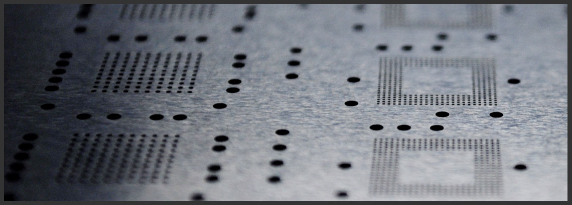
The printing phase in SMT assembly determines solder paste volume, placement accuracy, and joint reliability, forming the first line of defense against solder bridging and other PCB soldering defects. Engineers optimize aperture size and shape to regulate solder paste for each pad, while reducing aperture area on fine-pitch pads to prevent excess paste from creating bridges.
Laser-cut wall geometry with smooth, vertical edges releases solder paste efficiently during squeegee application and prevents smearing between pads. Stencil flatness and precise alignment ensure full contact with the PCB, maintaining consistent paste transfer on dense layouts and QFP or BGA packages.
Manufacturers design step stencils and variable aperture stencils for boards with varying pad sizes to control paste volume across multi-density layouts. JLCPCB laser cut stencils achieve micron-level aperture accuracy, maintain flatness, and repeat printing, producing reliable solder paste deposition for high-density SMT assemblies.
Practical Strategies to Eliminate Bridging During Production
Eliminating solder bridging during SMT assembly requires a combination of stencil optimization, printing discipline, and thermal control. Engineers adopt practical strategies to control solder paste deposition, maintain uniformity, and prevent electrical shorts between adjacent pads. These best practices address fine-pitch components, high-density layouts, and repeated production runs.
The key strategies to eliminate bridging during production are listed below:
1. Regular Cleaning Cycles:
Remove all residual solder paste from stencils after each print cycle. This prevents aperture clogging, ensures consistent paste volume, and reduces bridging risks across fine-pitch and high-density layouts. Proper cleaning maintains aperture wall smoothness and preserves stencil flatness for repeated production runs.
2. Choosing the Right Thickness:
Match stencil thickness to pad size, pitch, and component type. Thinner stencils limit paste volume on fine-pitch pads, reducing overflow between adjacent lands, while thicker stencils maintain sufficient volume for larger components to ensure complete solder joints. Correct thickness selection stabilizes paste transfer across the PCB.
3. Squeegee Optimization:
Set squeegee angle, pressure, and speed precisely for uniform paste transfer. Adjusting these parameters ensures consistent deposition across all pads, avoids smearing, and minimizes excess paste between pads. Optimized squeegee operation enhances repeatability in prototype and medium-volume runs.
4. Optimize Stencil Apertures:
Reduce aperture area by 10–20% for fine-pitch components. This limits solder paste volume, prevents accidental bridging, and maintains consistent joint formation. Properly designed apertures guide paste precisely to each pad without overflow or gaps.
5. Optimize Reflow Profile:
Adjust soak and peak temperatures to balance flux activation and solder melting. Controlled heating prevents aggressive flux boil-over that forces solder into gaps, minimizing the chance of hidden bridges under BGAs or QFPs. A stable thermal profile ensures complete and uniform joint formation.
6. Maintain Solder Mask Dams:
Preserve at least 0.1mm spacing between pads to contain solder paste. Proper mask dams act as physical barriers, reducing the risk of bridging across narrow gaps, particularly for fine-pitch ICs and dense connector arrays. Accurate mask design supports repeatable, defect-free printing.
Implementing these strategies consistently reduces solder bridging, improves joint reliability, and maximizes PCB assembly yield across both prototype and production boards.
Why JLCPCB Stencils Are the Best Choice for Short-Free Assembly?
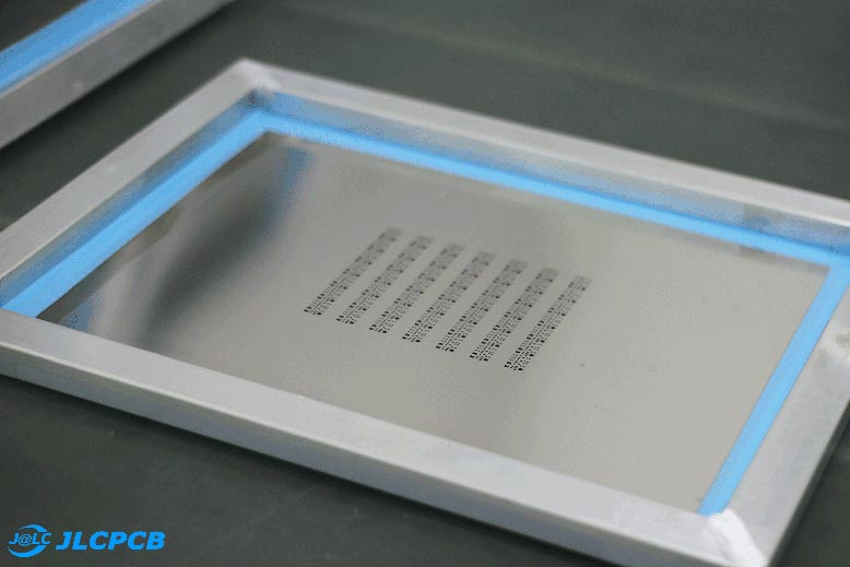
JLCPCB stencils provide high-precision, laser-cut apertures that maintain flatness and consistent wall geometry, controlling solder paste volume and reducing bridging and void formation during reflow. Electropolished walls improve solder paste release and allow repeatable deposition across fine-pitch ICs, BGAs, and high-density PCB layouts. Engineers rely on these stencils for both prototypes and medium-volume boards because their performance minimizes defects and improves joint reliability.
JLCPCB manufactures stencils using 304 HTA stainless steel and premium aluminum, achieving laser precision up to ±0.003mm. Framed and frameless (foil-only) options allow integration with manual or automated SMT printers. Advanced industrial processes, including nano-coating, electropolishing, step stencils, and ultrasonic-resistant adhesive, extend stencil lifespan while preserving aperture accuracy and flatness.
Online ordering starts at $3 USD, supports Gerber and DXF uploads, and delivers worldwide as fast as 12 hours. By providing fast, reliable, and precise stencil solutions alongside a current $11 JLCPCB coupon offer, we ensure highly accessible, defect-free SMT assembly for every engineer.
Conclusion: Achieving Perfect Yield With the Right Tools
Solder bridging is a manageable defect when engineers combine precise PCB layout with a high-quality stencil and disciplined printing process. Optimizing stencil apertures, wall geometry, and paste volume reduces bridging and improves electrical performance. Regular maintenance, cleaning, and correct reflow profiles maintain consistent solder paste deposition.
For reliable SMT assembly and high yield, engineers rely on JLCPCB stencil services for fast, high-precision stencils with consistent aperture geometry. Using professional-grade stencils simplifies prototype validation and production while minimizing defects—click here to claim your $11 JLCPCB stencil coupon and start your project today.
Frequently Asked Questions (FAQs)
How can solder bridging be prevented during reflow soldering?
Solder bridging can be prevented by controlling solder paste volume, optimizing stencil thickness and aperture design, ensuring accurate component placement, maintaining proper stencil cleaning cycles, and using a well-controlled reflow soldering profile.
How do you detect a PCB solder bridge?
A PCB solder bridge can be detected through visual inspection, automated optical inspection (AOI), X-ray inspection for hidden joints like BGAs, or electrical testing methods that check for unintended connections between pads.
Can a solder bridge be repaired?
Yes, a solder bridge can typically be repaired by removing excess solder using a solder wick, reworking the joint with flux, or carefully reheating the connection to separate the bridged pads.
Why do fine-pitch components increase the risk of solder bridging?
Fine-pitch components such as QFP, QFN, and BGA packages have very small spacing between pads and leads. During reflow soldering, even a small amount of excess solder paste can easily flow between these tight gaps and create a solder bridge.
Does stencil thickness affect solder bridging?
Yes, if the stencil thickness is too large, it deposits excessive solder paste on the pads. During reflow soldering, the extra solder can spread and create solder bridging between adjacent pads.
Is solder bridging a common SMT soldering defect?
Yes, solder bridging is one of the most common SMT soldering defects in PCB assembly, especially in high-density designs that use small components and fine-pitch packages. Proper stencil design and solder paste control are essential to minimize this issue.
Keep Learning
Manual Pick and Place: A Cost-Effective SMT Alternative
Key Takeaways for Manual Pick and Place Manual pick and place uses a hand-held vacuum wand and positioning stage to place SMD components by hand, replacing tweezers in prototype assembly. It is most cost-effective for production runs of 1 to 50 boards, where an automated SMT pick-and-place machine cannot justify its $10,000+ setup cost. A complete manual workstation runs $300 to $500, compared with $10,000+ for an entry-level automated pick and place machine. SMT stencil quality is the single largest ......
Hot Air Surface Mount Soldering: A Step-by-Step Guide
Key Takeaways Heat Control Is Everything: Hot air SMD soldering delivers uniform heat across all pads simultaneously, eliminating the lifted pads and cold joints common with iron-based soldering of fine-pitch components. Airflow Kills Small Parts: Set airflow to just 10–20% for 0402/0201 passives to avoid the Bernoulli Effect that turns tiny resistors into projectiles. Stencil Precision Prevents Tombstoning: A precision-cut SMT stencil deposits equal paste volume on both pads, balancing surface tensio......
Solder Paste Printing Defects: How Precision Stencils Prevent Assembly Failures
Key Takeaways 70% Rule: Approximately 70% of SMT defects originate from the solder paste printing stage, making it the most critical process to optimize. Root Causes: Defects like bridging, insufficient paste, misalignment, and slumping are caused by stencil tension, process parameters (pressure, speed), and paste chemistry/environment. Area Ratio Matters: Maintaining an aperture Area Ratio (AR) above 0.66 (per IPC-7525) is essential to ensure proper paste transfer efficiency and prevent chronic insuf......
Best Manual Pick and Place Tools for Precise PCB Assembly
While fully automated robotic SMT lines handle mass production efficiently, every hardware innovation begins on a workbench. Engineers shifting from soldering large through-hole components to microscopic surface-mount devices (SMD) by hand quickly realize that precision and control are everything. Achieving factory-level assembly on your desk is absolutely possible with the right setup. This guide reviews the essential tool categories needed to build an effective prototyping workbench, covering precis......
How to Use a BGA Stencil for SMT Assembly and Reballing (Design & Process Guide)
Anyone who's spent time in a lab knows the look. You flip over a BGA chip and stare at the bottom. Flat. Featureless. No legs. No leads. Just a grid of tiny silver bumps. First thought? How the hell am I supposed to solder this? The Ball Grid Array (BGA) package is a trade-off. You get insane I/O density in a tiny footprint. But every single connection is hidden. You can't see them, and you can't poke them with an iron. Here's the thing I learned after lifting more pads than I'd like to admit: learnin......
Solder Bead Prevention: How PCB Stencil Design & Process Control Deliver Defect-Free Reflow Soldering
In modern SMT assembly, solder joint quality is determined long before the reflow oven starts—at the solder paste printing stage. When this step is not properly controlled, the consequences appear after reflow as tiny spherical solder particles scattered around component pads: solder beads. For engineers working with high-density assemblies, these defects are familiar and frustrating because they reappear whenever a process variable drifts outside its optimum range. This guide takes an engineering-fir......