
Flex PCB Prototyping Guide: Materials & Design Tips
11 min
- Understanding Flex PCB Prototyping
- Material Selection for Flex PCB Prototypes
- Flex PCB Design and Panelization Guidelines
- Choosing Suitable Stiffeners for Flex PCB Applications
- Frequently Asked Questions (FAQ)
Key Takeaways
A reliable flex PCB prototype requires more than just a working circuit. Material selection, bend radius control, copper design, panelization, and stiffener choices directly impact flexibility, durability, and manufacturing success. By following proper flexible PCB prototyping practices, engineers can reduce design risks and smoothly transition from prototypes to production with JLCPCB.
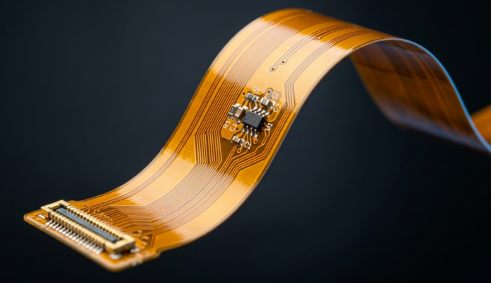
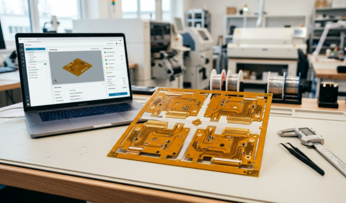
Ever wonder how the circuit in a smartwatch, a foldable phone, or a camera module can take the shape? The key is a flexible printed circuit (FPC) underneath. Producing a sample flex PCB that works is the name of the game. Flex circuits are very different from rigid FR4 boards. They bend, twist, and wrap around small spaces, and this requires new thinking about materials, routing of traces, and even panelization.
If you do not include these details in the prototype, you'll end up paying for it with broken traces and failed assemblies. In this article, we will go through the real-world aspects of flexible PCB prototyping. You will know how to select the correct base material, control the bend radius, and stress. To increase yield and to easily transition from a single prototype into volume production, panelize the PCB.
Understanding Flex PCB Prototyping
Unlike a rigid laminate, a flex PCB is fabricated on a thin film substrate that is flexible. That film is then bonded to a copper foil with a conductor pattern etched into it, and the whole thing is covered by a protective coverlay. This type of construction is the key to the board's ability to flex, roll, and transfer mechanical motion.
The purpose of a flex PCB prototype is to test three things in one go: functionality, fit, and manufacturability. A flex prototype cannot be as rigid as a rigid board, because they need to demonstrate they can withstand the flexing they're expected to endure. If the circuit functions as expected on the bench but fails after 100 flex cycles, it is considered to have failed the prototype stage. Flex stack-ups are very thin and fragile, so little things are important. The location of one hole or the routing of a single trace within a bend area can determine the life of your board; for example, thousands of cycles versus failure at the first bend.
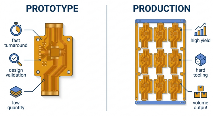
Differences Between Prototype and Production Flex PCBs
The prototype is about rapid learning, and the production is about repeatable yield. Both stages are the same in materials but optimized for different things. Knowing this difference helps to ensure your initial samples are not misleading. One of the most frequent errors is that of prototyping one board, but not considering the panel context. Your prototype should also be configured in the same way(s) as production will be configured (panels with rails and tooling holes, for example) to expose the DFM issues at a smaller scale instead of at scale-up.
Common Challenges in Flexible PCB Prototyping
Failure modes unique to flexible PCB prototyping are being introduced. That's the whole idea of a prototype: to catch them early. These are the problems most newbie flex designers have:
- Copper traces running perpendicular to the fold line at the bend zones, resulting in cracks.
- When adhesive selection and cure schedules are incorrect, coverlay delamination occurs.
- By cracking the plate holes in the dynamic bend area.
- Thin polyimide can tear and crease easily during assembly, which can cause handling damage.
- The controlled impedance is sensitive to small changes in thinness, so there is the possibility of impedance drift.
Material Selection for Flex PCB Prototypes
The base of a reliable flex prototype is material choice. Together, the base film, copper type, and adhesive system determine the flexibility, durability, and thermal stability of your board. As the first layer before routing anything, it is a layer to get right. The two most important choices are the dielectric film and the copper foil. Select a film for the application environment and flex demands, and then select copper for current and bending requirements.
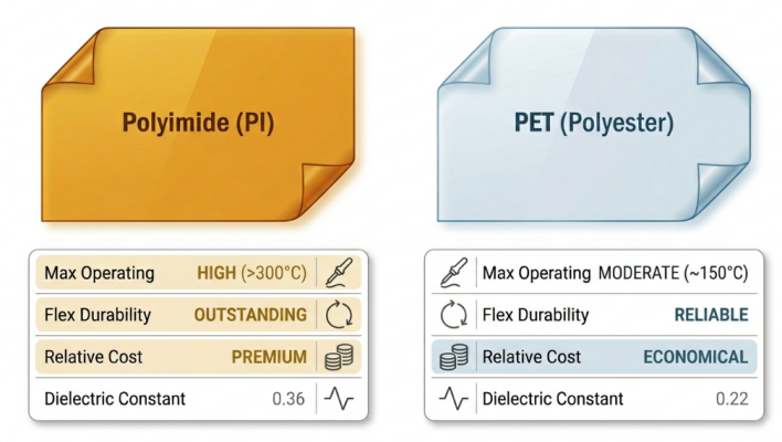
Polyimide vs PET Material Comparison
The workhorse of professional flex circuits is polyimide (PI). It can endure repeated flexing, soldering temperatures, and repels chemicals. PET (polyester) is less expensive and is suitable for low-cost, low-temperature applications, but not reflow soldering.
| Property | Polyimide (PI) | PET (Polyester) |
|---|---|---|
| Max temperature | Up to ~260 °C (solderable) | ~150 °C, not reflow-safe |
| Flex durability | Excellent, dynamic flex | Moderate, static flex |
| Cost | Higher | Lower |
| Typical use | Wearables, medical, aerospace | Membrane switches, throwaway sensors |
| Dielectric constant (Dk) | ~3.2-3.5 | ~3.0-3.3 |
If you're choosing between polyimide and polyester, just remember that polyimide is the material of choice for nearly any prototype that will be soldered or bent multiple times. Use PET for low temperature, low cost, static products, in which the circuit would be assembled using conductive adhesive, not reflow.
Copper Thickness and Flexibility Considerations
There are two flavors of copper that have definite effects on flex life. Rolled annealed (RA) copper has an elongated grain structure that bends much farther than electrodeposited (ED) copper. RA copper is highly recommended for use in any dynamic flexing application. Most flex prototypes use light copper weights as they are easier to bend and have a greater number of flex cycles. Common choices include:
- 1/3 oz (12 µm) for fine-pitch, high-flex-life dynamic applications.
- 1/2 oz (18 µm) as a balanced default for most signal flex circuits.
- 1 oz (35 µm), where higher current is needed, and bending is occasional or static.
Note that both a thin dielectric and a thin copper will increase flexibility as well as decrease mechanical strength. The key to flexible PCB prototyping is balancing flex life with the current handling and durability that is required for your application.
Flex PCB Design and Panelization Guidelines
Good flex design takes into account the mechanics of bending from the first trace. How long the board lasts in the field is directly dependent on the layout rules you follow. Use the bend zone as an area that has its own rules and is not affected by the rigid-style routing. Panelization then dictates the efficiency of manufacturing and assembly of those boards. Smart panel layout can help to optimize SMT yield and reduce cost per unit even in prototype quantities.
Bend Radius, Trace Routing, and Stress Relief
Bend radius is the one thing that is most critical in flex design, mechanically. Any bend that is too severe will focus stress and cause the copper to crack. To give a good rule of thumb, the minimum bend radius is a minimum of 6 times the total thickness of the material for single-sided dynamic flex and 10-12 times the total thickness of the material for double-sided dynamic flex. There are a few rules that are non-negotiable when it comes to routing in the bend area. These and most flex failures simply disappear:
- Route traces in perpendicular direction and parallel to the bend, copper is flexed along the length, not across the bend.
- Traces should be at right angles to the bend line, not diagonal.
- No vias, pads, or plated holes within the dynamic bend zone.
- Avoid sharp corners in traces and make them curve to distribute stress evenly.
- Stagger traces on alternate layers to avoid creating a direct copper over-bend (neutral-axis).
Panelization Methods for Better Material Utilization
Panelization is all about maximizing the board usable from a sheet of flex material, which is costly. The selection of the right method to be adopted is determined by the shape, flexibility, and use of the board in SMT.
| Method | Best For | Trade-off |
|---|---|---|
| Tab routing | Rigid-flex, sturdier panels | Tabs need clean removal |
| Perforation (mouse bites) | Small flex boards | Leaves rough edges |
| Carrier frame | Thin, floppy flex in SMT | Extra material and cost |
| Nested layout | Irregular flex shapes | Needs careful CAM work |
Some practices have positive impacts on yield and material use. When cutting out the pieces of an irregular panel, nest them like puzzle pieces to minimize waste, add fiducials and tooling holes on the rails to support accurate placement, and add a stiffener or carrier to keep a flex panel flat through the pick-and-place machine.
Choosing Suitable Stiffeners for Flex PCB Applications
A stiffener is a stiffener that is bonded to specific areas of a flex circuit. Provides mechanical support under connectors, components, or ZIF insertion zones when flatness is required. The remaining board is free to flex. The selection of a stiffener is a compromise between mechanical requirements and cost. The type of material, thickness, and bonding technique are relevant, and overspecifying is a waste of money.
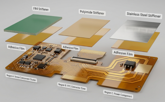
FR4, PI, and Stainless Steel Stiffener Options
The materials used in stiffeners are for specific purposes. Make sure the material matches the job; don't use the same material everywhere on the board.
| Stiffener | Typical Thickness | Best Use |
|---|---|---|
| FR4 | 0.2-1.6 mm | Component mounting, mechanical rigidity |
| Polyimide (PI) | 0.05-0.225 mm | ZIF/FPC connector insertion zones |
| Stainless steel | 0.05-0.3 mm | Thin, strong support; heat spreading |
Balancing Mechanical Support and Manufacturing Cost
The greater the stiffener area, the thicker the material, the more expensive and time-consuming it is to get the material. The intelligent thing to do is to stiffen only what really needs it. Consider if each region needs support or if Flex can manage the load? Here are some tips for saving money:
- Time-consuming areas that are intended to be in contact with the components.
- Do not overbuild connectors, and match stiffener size to the connector specification.
- PSA (Pressure sensitive adhesive) is used for prototypes for fast turnaround.
- Use a limited number of stiffener sizes for ease of tooling.overbuildFlex PCB Manufacturing and Prototyping Services
When the manufacturer is ready for it, it is much easier to get a flex design to become a turnaround piece. The flexible PCB processes provided by modern PCB manufacturers like JLCPCB can take you from one flexible PCB prototype to full production, all without changing partners. This continuity is a definite plus if your design changes. Prototyping benefits are quick turnaround time, low cost, and design feedback prior to tooling commitment. That combination allows you to easily make rapid changes to bend zones, stiffeners, and stackup.
Flexible Material and Manufacturing Options
The construction of the flex PCB is polyimide, and JLCPCB's flex PCB service is designed based on it, which can meet most prototype needs. Common features related to flexible PCB prototyping include:
- Copper rolled annealed types are appropriate for bending.
- Coverlay with stiffener support, such as FR4 or PI stiffeners.
- Surface finishes like ENIG for fine pitch and reliable solderability.
- Low entry pricing and 1-2 day production for fast iteration.
These alternatives allow you to design a realistic version of your end board, not a simple stand-in. Your test results on production-grade polyimide and copper are volume results.
DFM Support from Prototype to Production
Large flex projects are the most perilous because of the potential for finding a manufacturability issue after scaling up. Bend-zone vias, tight radii, and panelization issues are detected early in a good DFM review during the prototyping phase. Many of these are caught by automated DFM checks and instant quoting by JLCPCB before getting to the production line. JLCPCB's flexible PCB service makes it easy to order a sample, get the DFM feedback, and then scale up the same design to production. By keeping prototype and production on one process, you will minimize surprises and shorten your development cycle altogether.

Frequently Asked Questions (FAQ)
Q: What is the minimum bend radius for a flex PCB prototype?
Ans: A common rule of thumb is at least 6 times the total board thickness for single-sided dynamic flex, and 10-12 times for double-sided designs. Tighter radii concentrate stress and risk cracking the copper, so always validate the bend on a real prototype.
Q: Should I use polyimide or PET for my flex PCB prototype?
Ans: Use polyimide for almost any prototype that will be soldered or flexed repeatedly, since it handles reflow temperatures and high flex cycles. Reserve PET for low-cost, low-temperature, static applications like membrane switches.
Q: Why is rolled annealed copper preferred over electrodeposited copper in flex circuits?
Ans: Rolled annealed (RA) copper has an elongated grain structure that withstands bending far better than electrodeposited (ED) copper. For any dynamic flexing application, RA copper greatly improves flex life and reduces cracking.
Q: Do I need a stiffener on my flex PCB?
Ans: You need a stiffener wherever the board must stay flat, such as under connectors, components, or ZIF insertion zones. Use FR4 for general rigidity, PI for FPC connector zones, and stainless steel for thin, strong support, but stiffen only the regions that require it.
Q: How does panelization affect flex PCB prototyping cost?
Ans: Smart panelization nests boards to reduce expensive flex material waste and improves SMT yield by keeping limp panels flat during assembly. Even at prototype quantities, using carriers, fiducials, and nested layouts makes scaling to production smoother and cheaper.

Popular Articles
• 45 Must-Know Flex PCB Design Tips You Can't Afford to Miss!
• Choosing the Right Bend Radius for Durable Flexible PCBs
• FPC Design Rules: 13 Safety Distances You Can’t Ignore
• Mastering PCB Stiffeners: A Comprehensive Guide to Types, Applications, and Design Best Practices for Flexible Circuits
• How Flex Coverlay Protects and Enhances Flexible PCB Durability
Keep Learning
Flex PCB Manufacturing Process: From Prototyping To Mass Production
Flexible Printed Circuit Board commonly known as flex PCBs are a revolutionary step in modern electronics that offer compact, lightweight, dynamic and precise designs. Flex PCBs are designed to bend, twist, and fold, which rigid boards are incapable of. These characteristics have led to their widespread adoption in industries like wearable technology to consumer electronics to aerospace and medical technologies. With demands increasing day by day for miniaturized and ergonomic product designs, underst......
45 Must-Know Flex PCB Design Tips You Can't Afford to Miss!
Achieving perfection in product design requires a careful balance between meeting design requirements and manufacturing standards. However, when it comes to flex PCB (FPC) design, many engineers find themselves at a loss, unsure of where to begin. In this insightful guide, we will delve into 45 essential design guidelines for FPC. By the end, you'll have the knowledge and confidence to navigate the complexities of flex PCB design. Outline and Drilling 1. The minimum distance from through-holes to the ......
Choosing the Right Bend Radius for Durable Flexible PCBs
Key Takeaways Mastering the bend radius is essential for reliable flexible PCB design. Following IPC-2223 guidelines, maintain a minimum of 6× total thickness for static bends and 100× for dynamic applications, while using thinner RA copper, adhesiveless polyimide, staggered traces, and cross-hatched patterns in flex zones. Proper material selection, layer stackup optimization, and adequate clearance from stiffeners can dramatically extend flex life and prevent premature trace cracking or delamination......
FPC Connector Guide: Types, Pitch & Reliability
Key Takeaways Choosing the right FPC connector is critical for reliable flexible electronic designs. Connector type, pitch, pin count, stiffener thickness, and PCB layout all affect signal integrity and mechanical durability. By understanding FPC connector selection and design considerations, engineers can reduce connection failures and achieve reliable assembly results with JLCPCB. As you know, the electronics world is getting smaller; nowadays, the devices need to be thin and light. All the parts sh......
Flex PCB Design Guide: Preventing Mechanical Failures
Key Takeaways Reliable flex PCB design requires more than electrical performance. Proper bend radius control, trace routing, via placement, stiffener selection, and DFM considerations are essential to prevent mechanical failures such as copper cracking and delamination. By following proven flexible PCB design practices, engineers can improve durability and achieve reliable production results with JLCPCB. Ever wonder how the circuit in a foldable phone, fitness tracker, or camera module manages to rema......
Flex PCB Prototyping Guide: Materials & Design Tips
Key Takeaways A reliable flex PCB prototype requires more than just a working circuit. Material selection, bend radius control, copper design, panelization, and stiffener choices directly impact flexibility, durability, and manufacturing success. By following proper flexible PCB prototyping practices, engineers can reduce design risks and smoothly transition from prototypes to production with JLCPCB. Ever wonder how the circuit in a smartwatch, a foldable phone, or a camera module can take the shape? ......