Best Flex PCB Design Software: CAD Tools & Setup Guide
19 min
- What Is Flex PCB Design Software?
- Key Software Features Required for Flexible PCB Design
- Best Flex and Rigid-Flex PCB Design Software Compared
- How to Set Up a Flex PCB Design in CAD Software
- Flex PCB Design Rules: Bend Radius, Routing, and Stiffeners
- Design for Manufacturing and Fabrication File Generation
- Common Flex PCB CAD Design Mistakes and How to Avoid Them
- Conclusion
- FAQs About Flex PCB Design Software
The right flex PCB design software would rely on the complexity and construction of your circuit. Altium Designer, Cadence Allegro X, OrCAD X, and Siemens Xpedition are professional tools that offer advanced capabilities for flexible and rigid-flex PCB designs, such as stackup management, bend regions, and mechanical constraints. In the meantime, for more basic flexible circuits, tools such as KiCad or EasyEDA Pro might be viable options, though they may require some manual setup and verification. Flexible circuits, unlike traditional rigid PCB designs, require special attention to areas such as bend zones, coverlay openings, stiffener placement, and material properties to ensure manufacturability and reliability.
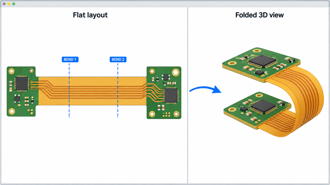
Figure: Flex PCB design software showing the same rigid-flex board in its flat layout and its folded 3D form.
This guide will explain which CAD features are crucial for flexible and rigid-flex PCB design, the differences between the native capabilities and workarounds of six popular PCB design tools, and how to set up stackups, bend lines, and keep-outs in your design software.
What Is Flex PCB Design Software?
Flex PCB design software is PCB CAD software used to define the copper layout for a flexible circuit, as well as the flexible stackup, bend areas, coverlay openings, and stiffeners. Most PCB editors can route copper on a thin board. Additionally, a flex design requires a tool to specify the board configuration and the bending point.
How Flex PCB Design Software Works
A flex PCB design tool requires completing three tasks, which can be omitted by rigid-board layout:
- Layer stackup management: Stores the thicknesses of the polyimide, adhesive, copper, and coverlay layers. Rigid-flex tools provide a different stackup for each region of a board.
- Definition of bend region: Indicate placement and routing rules where the circuit bends, its radius, and angle.
- Manufacturing documentation: Provides the fabricator with coverlay, stiffener, outline, and stackup data.
A flex PCB consists of just flexible materials and optional bonded stiffeners. A rigid-flex PCB is a type of PCB lamination that incorporates flexible layers within rigid multilayer segments, linking them via plated through-holes. Not many PCB editors natively support rigid-flex modeling.
Rigid PCB vs. Flex PCB CAD Workflows
With a rigid board, a single stackup is applied throughout the entire outline, and electrical DRC encompasses most of the review. An added mechanical decision is added with a flex or rigid-flex design that the CAD data must also convey:
The right flex PCB design software would rely on the complexity and construction of your circuit. Altium Designer, Cadence Allegro X, OrCAD X, and Siemens Xpedition are professional tools that offer advanced capabilities for flexible and rigid-flex PCB designs, such as stackup management, bend regions, and mechanical constraints. In the meantime, for more basic flexible circuits, tools such as KiCad or EasyEDA Pro might be viable options, though they may require some manual setup and verification. Flexible circuits, unlike traditional rigid PCB designs, require special attention to areas such as bend zones, coverlay openings, stiffener placement, and material properties to ensure manufacturability and reliability.
This guide will explain which CAD features are crucial for flexible and rigid-flex PCB design, the differences between the native capabilities and workarounds of six popular PCB design tools, and how to set up stackups, bend lines, and keep-outs in your design software.
| CAD Task | Rigid PCB Workflow | Additional Flex PCB Requirement |
| Stackup | One stackup for the full board | Flex stackup with coverlay and adhesive, plus a stackup per region for rigid-flex |
| Board outline | One routed outline | Rigid regions, flex regions, and transition zones |
| Mechanical fit | The board fits a flat envelope | Bend location, radius, angle, and fold order |
| Design rules | Electrical width and clearance | Via, pad, and component exclusion in bend zones |
| Local support | Rarely needed | Stiffener outlines, materials, and thickness |
| Fabrication data | Copper, mask, drill, and outline | Coverlay openings, stiffener layers, and a stackup drawing |
Key Software Features Required for Flexible PCB Design
The features that matter in flexible PCB CAD software are region-specific stackups, bend definition with 3D folding, flex-aware design rules, and complete manufacturing output.
Multi-Zone Stackup Management and Flex Region Definition
Rigid-flex PCB design software allows assigning a stackup to each board region, rather than to the entire board outline. The rigid area could be four copper layers on FR-4, and the flex area next to it could be two copper layers on polyimide with coverlay.
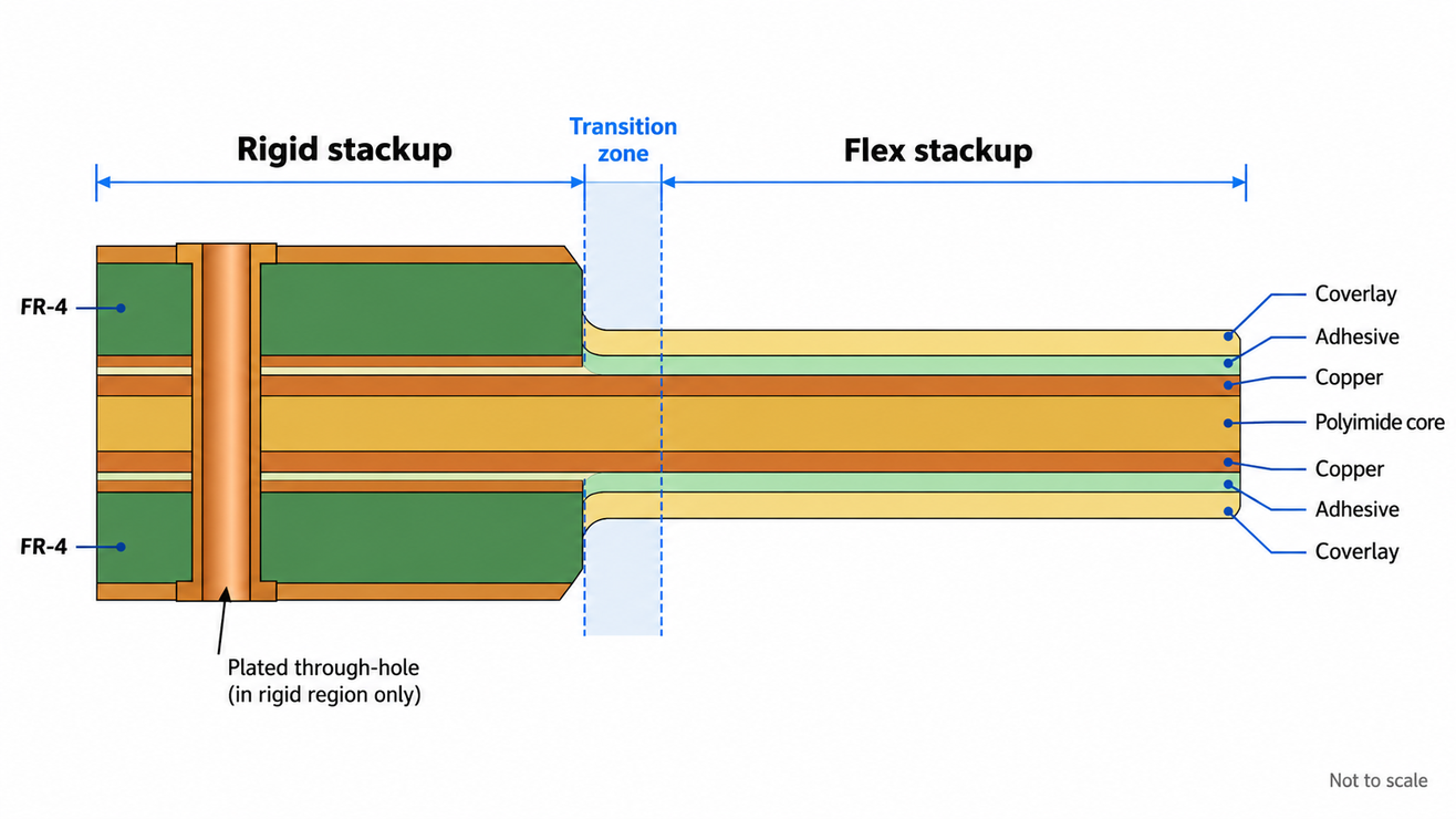
Figure: Flex PCB design software stackup zones showing a rigid region, a flex region, and the transition between them.
For each region, the software keeps:
- The copper layers present and their thickness
- Each dielectric and adhesive layer, with material and thickness
- Coverlay or flexible solder mask over the flex area
- The boundary where one stackup transitions to the next
The stackup is stored per region and kept at the same thickness, impedance values, and 3D model as the board being built.
3D Bending, Folding, and Mechanical Fit Verification
A bend line marks the fold axis, and its properties set the bend radius and bend angle. A fold order determines the sequence in which several bends interact. The fabricator builds the unfolded layout; the folded 3D view, shared through STEP or a direct ECAD-MCAD link, shows the enclosure fit.
Flex-Specific Design Rules and Material Configuration
Flex-aware PCB CAD software lets design rules target flex and bend regions separately from rigid areas. Check that the tool supports:
- Region-scoped rules: Trace width, spacing, and via rules that apply only inside a named flex region.
- Bend-zone keep-outs: Objects that block vias, pads, and components inside a bend area.
- Hatched copper fills: Zone fills that keep copper planes flexible.
- Teardrops: Automatic teardrops at the pad and via connections.
Material configuration includes the polyimide base, the type of laminate (rolled-annealed (RA) or electrodeposited (ED) copper, coverlay, and stiffener material). In repeated flexing, RA copper is the preferred choice. These entries go into the stackup drawing and should correspond to the available materials the fabricator can provide.
IPC-2223 Design Guidance and Manufacturing Output Support
IPC-2223 is the standard for sectional design of flexible and rigid-flex printed boards. Its guidance and the fabricator's abilities are translated into CAD rules by engineers. A CAD tool will enforce rules entered by the designer, but cannot certify IPC-2223 compliance. Output support determines how much data portions of the construction are output to the fabricator instead of notes:
- Gerber X2: Layer images with attributes that identify each file's function. A separate Gerber job file carries characteristics such as finish, overall thickness, and materials.
- ODB++: A database of files containing fabrication and assembly data.
- IPC-2581: An XML-based format containing fabrication and assembly data in a single file.
Best Flex and Rigid-Flex PCB Design Software Compared
KiCad and EasyEDA Pro are well-suited to simpler flex constructions; the best flex PCB design software for rigid-flex is Altium Designer, Cadence Allegro X, OrCAD X, and Siemens Xpedition. The PCB Design Tools Guide compares these tools for general PCB work.
1. Altium Designer
There are two rigid-flex modes in Altium Designer. Standard mode divides a flat board shape into sections with split lines. The documentation for rigid-flex, provided by Altium, includes information on the following additional features in advanced mode: overlapping flex regions, coverlay on a flex region, bookbinder structures, and flex-only boards.
- Layer Stack Manager: Defines substacks and assigns one to each board region.
- Bending lines: Placed in Board Planning Mode, with a bend radius, bend angle, and fold index that sets the folding order.
- 3D folding: A Fold State slider switches the board between flat and folded states.
- MCAD collaboration: CoDesigner passes board shape and component changes between ECAD and MCAD.
Altium states that the available features depend on the licensed solution. It suits product teams that need native rigid-flex design.
2. Cadence Allegro X and OrCAD X
According to Cadence, OrCAD X PCB Layout and Allegro X PCB Designer offer region-specific stackups, control over layer transitions, bend-aware routing, and folded 3D visualization.
- Stackup zones: The cross-section editor holds multiple cross-sections, one for each rigid or flex zone, as described in Cadence's inter-layer checks white paper.
- Inter-layer checks: In-design checks between flex layers and objects, such as coverlay to pad, bend area to via or component, and stiffener to bend area.
OrCAD X and Allegro X products and licenses have different feature depth—check with Cadence for confirmation. The tools are appropriate for designs that have numerous stackup zones and dense rule sets.
3. Siemens Xpedition
In Xpedition, a rigid-flex design starts with multiple named board outlines, each assigned its own layer stackup, according to Siemens' rigid-flex PCB design page.
- Bend areas: A dedicated "bend area" object defines where the board bends.
- Region rules: Via, trace, and plane-type rules apply per region.
- Contour routing: Routing follows a curved flex outline.
- Visualization: An integrated 2D and 3D environment shows the design.
Xpedition fits enterprise teams building complex multi-region assemblies. Confirm which rigid-flex functions a given license includes.
4. KiCad
KiCad is free, open-source software for laying out a flex circuit. KiCad 10 PCB Editor documentation does not mention a stackup for the entire board or a bend-line object, so rigid-flex regions and bends are not modeled natively. The stackup is designed to work with only even numbers of copper layers: a single-layer flex circuit is configured as two layers with one unused.
A KiCad flex workflow relies on:
- User layers: Stiffener outlines and bend lines, named for the fabricator.
- Rule areas: Keep vias and footprints out of bend zones, and apply custom DRC rules to named areas.
- Hatched zones and teardrops: Built-in zone and routing options.
- Outputs: Gerber, drill files, IPC-2581, and ODB++.
KiCad suits basic flex prototypes when the stackup and bend requirements are handled in a separate fabrication drawing.
5. EasyEDA Pro
EasyEDA Pro has an FPC work process documentation. The layer manager will change the board type to FPC and add two layers of stiffeners when a stiffener is added to a rigid PCB project.
- Stiffener properties: Material and thickness set per stiffener: PI, steel, 3M double-sided tape, or EMI shielding film.
- Outputs: Stiffener data is automatically added to the exported Gerber files.
- Layer naming: Prefixes such as pit_0.25 (0.25 mm PI, top) follow the FPC stiffener layer naming guide.
The documented workflow covers FPC layout and stiffeners, not multi-stackup rigid-flex or folded 3D modeling, so it suits simple flex PCB projects.
6. Autodesk Fusion
Autodesk Fusion combines PCB design and mechanical CAD. According to the Autodesk Support article “How to create Flex and Rigid-Flex PCB boards in Fusion,” rigid-flex is not supported natively, but it describes a workaround in which a STEP model of the board is bent. The bent model is intended to help verify enclosure fit, but the stackup and flex rules are still in effect for user layers and drawings. Fusion is not for rigid-flex production layout; it's for mechanical concept visualization.
Flex PCB Design Software Comparison Table
| Software | Independent Region Stackups | Native Bend Modeling | Flex-Specific Checks | Stiffener Definition | Best Suited For |
| Altium Designer | Yes | Yes | Partial: region-scoped rules | Verify by edition | Professional rigid-flex products |
| Cadence Allegro X / OrCAD X | Yes | Yes | Yes: inter-layer checks, verify by edition | Yes | Constraint-heavy rigid-flex designs |
| Siemens Xpedition | Yes | Yes | Yes: region rules | Verify by edition | Complex multi-region assemblies |
| KiCad | No | No | Partial: rule areas and custom rules | Manual: user layer | Basic flex prototypes |
| EasyEDA Pro | No | No | Standard DRC; no flex rules documented | Yes: FPC stiffener layers | Simple flex PCB projects |
| Autodesk Fusion | No | Workaround: bent STEP model | No | Manual: user layer | Mechanical concept visualization |
How to Set Up a Flex PCB Design in CAD Software
The flex PCB layout process is divided into five steps: region definition, stackup configuration, bend line addition, rule scope, verification, and export. The menu names and capabilities vary by rigid-flex PCB layout software; the names used here are those native to Altium.
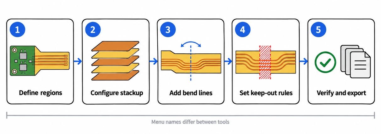
Figure: Flex PCB design software setup workflow in five steps, from board regions to fabrication output.
Step 1: Define Board Geometry and Rigid and Flex Regions
- Import the mechanical outline: Bring in the board shape and keep-out zones from MCAD as DXF or STEP.
- Divide the outline into regions: mark each rigid island and flex section using split lines or separate region objects, as the tool requires.
- Fix connector locations: Place connectors first, because they set the flex length and stiffener positions.
Step 2: Configure the Flexible PCB Stackup
- Create the flex stackup: Enter polyimide, adhesive, copper, and coverlay thicknesses from the fabricator's stackup options.
- Create the rigid stackups: For rigid-flex, build the rigid layers around the shared flex layers.
- Assign stackups to regions: Link each region to its stackup so thickness and impedance values stay correct.
- Record the copper type: Note RA or ED copper for each flex layer.
The flex PCB stackup design guide explains how each layer adds to the total thickness.
Step 3: Add Bend Lines and Define Mechanical Constraints
- Place each bend line: Locate it on the fold axis inside a flex region.
- Set the radius and angle: Use the calculated inside bend radius and the angle from the enclosure model.
- Set direction and fold order: Set which side folds inward, and the fold order where bends overlap or stack.
- Check the folded fit: Fold the board in 3D and confirm clearance to the housing.
Step 4: Configure Routing, Placement, and Keepout Rules
- Draw bend-zone keep-outs: Cover the bend arc plus a margin on each side, excluding vias, pads, and components.
- Scope trace rules to flex regions: Set width and spacing for the flex copper thickness.
- Set copper rules: Use hatched fill and teardrops in flex areas.
- Restrict component placement: Limit components in flex regions to stiffener-supported areas, unless the fabricator approves otherwise.
Step 5: Verify the Layout and Export Manufacturing Data
- Run electrical DRC: Clear width, clearance, and connectivity errors.
- Review the flex regions: Check keep-outs, trace direction, and coverlay openings.
- Inspect the folded assembly: Use the 3D fold view where the tool supports it.
- Export the fabrication package, including copper, coverlay, stiffener, drill, and outline data, with a stackup drawing.
- Obtain fabricator sign-off: Resolve engineering questions before release.
Flex PCB Design Rules: Bend Radius, Routing, and Stiffeners
CAD constraints apply to flex PCB design guidelines: bend radius, keep-out areas, region-scoped routing rules, and stiffener layers. The mechanical reasons explain each rule in the flex PCB design guide.
Calculating Bend Radius in PCB Design Software
Bend radius calculation software or a spreadsheet begins with the preliminary relationship R_min = k × t, where t is the finished thickness of the bend region, and k is a multiplier determined by the construction and application. A static flex is bent at installation and retained. A dynamic flex is a flex in which the movement occurs repeatedly, like a hinge.
There are two sets of multipliers released by JLCPCB. The flex PCB capabilities page provides the minimum, and the flexible PCB bend radius guide provides the conservative values:
| Application | Minimum Multiplier | Conservative Multiplier |
| Static, single layer | 6× | 6× |
| Static, multilayer | 10× | 12× |
| Dynamic | 10–15× | 100× single layer, 100–150× multilayer |
Use the minimum only where the enclosure leaves no room for more. Use the conservative value whenever space allows, and for any dynamic bend that cycle testing has not validated.
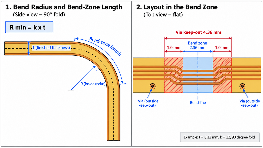
Figure: Bend radius calculation in flex PCB design software showing inside radius
Worked example. Assumptions: a static bend on a double-sided flex (two copper layers, so the multilayer row applies), 0.12 mm finished thickness in the bend region,n including coverlay, and a 90° fold.
- Minimum radius: 10 × 0.12 mm = 1.2 mm
- Conservative radius: 12 × 0.12 mm = 1.44 mm
- Bend-zone length at the mid-thickness radius: (π/2) × (1.44 + 0.06) mm ≈ 2.36 mm
- Via keep-out width: 2.36 mm plus the guide's 1.0 mm static clearance on each side ≈ 4.36 mm
Trace Routing and Copper Management in Flex Zones
Apply these practices in the flex regions. Teardrops and hatched fills are tool settings, while trace direction and layer staggering are usually confirmed in the flex-region review of Step 5:
- Cross the bend at right angles: Traces routed generally perpendicular to the bend line take the shortest path through the strained area.
- Use smooth transitions: curved corners and gradual changes in width avoid stress concentrations.
- Stagger adjacent layers: Traces stacked directly on top of each other form an I-beam that stiffens the bend.
- Add teardrops: Teardrops at the pad and via connections spread stress across the joint.
Defining Stiffeners, Coverlay Openings, and Transition Zones
Each stiffener is an outline filled on individual layers, one layer per material, thickness, and side:
- FR-4: Rigid backing for connector areas and through-hole parts.
- Polyimide: Control of thickness under ZIF-connector contacts.
- Stainless steel: Thin and flat supporting material for SMT components. JLCPCB says that steel itself is slightly magnetic, so Hall-effect sensors should avoid it.
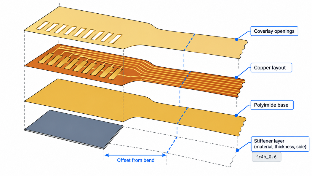
Figure: Flex PCB stiffener and coverlay layers aligned to the copper layout at a connector and a rigid-to-flex transition.
Add openings for coverlay on the solder mask layers or on a separate layer, and label the layer in the fabrication notes. Check whether the fabricator applies its coverlay expansion (JLCPCB: 0.1 mm per side) or if it must be included in the data. Avoid placing stiffener edges and/or stiffener-to-flex transition on bend lines because the stiffener-to-flex change will not occur on the bend line.
Flex-Specific DRC Checks Before Manufacturing
Flex checks fall into four groups:
- Automated in most tools: Via and component exclusion in bend keep-outs, width and clearance by region, and copper-to-edge clearance.
- Automated in rigid-flex tools: Coverlay-to-pad, stiffener-to-bend, and zone-transition checks, where inter-layer checks exist.
- Manual review: Stackup drawing versus CAD stackup, bend direction, and stiffener thickness versus the connector datasheet.
- Fabricator confirmation: Minimum radius for the chosen materials, coverlay registration, and stiffener tolerances.
Design for Manufacturing and Fabrication File Generation
A flex design is ready for fabrication when its files describe the whole construction in a format the fabricator accepts.
Gerber X2 vs. ODB++ vs. IPC-2581 for Flex PCBs
| Format | What It Carries | Flex Handoff Consideration |
| Gerber X2 | Layer images with file-function attributes, plus an optional Gerber job file | Valid for flex and rigid-flex when coverlay, stiffener, and stackup drawings are complete |
| ODB++ | A database of fabrication and assembly data | Reduces layer interpretation if the fabricator accepts it |
| IPC-2581 | An XML file with fabrication and assembly data | Open format with the same benefit, if the fabricator accepts it |
Common Flex PCB CAD Design Mistakes and How to Avoid Them
Flex CAD errors usually stem from an incomplete setup: an incorrect stackup, an unchecked bend, or files that omit flex requirements.
Incorrect Stackups and Unsupported Bend Constraints
| Mistake | Consequence | Correction |
| Rigid stackup applied to the flex region | Wrong thickness, bend radius, and impedance | Assign a flex stackup to each flex region |
| Adhesive or coverlay thickness omitted | Bend radius sized on too thin a section | Use the finished thickness of every layer |
| 3D fold accepted as proof of reliability | Cracked traces after repeated bending | Validate dynamic bends with flex-cycle testing |
Conclusion
The selection of the appropriate flex PCB design software depends on the complexity of your circuit, stackup requirements, and budget. For more complex rigid-flex designs, specialized software such as Altium Designer, Cadence Allegro X, OrCAD X, and Siemens Xpedition offers features and tools tailored to rigid-flex boards. At the same time, KiCad and EasyEDA Pro are suitable for simpler, flexible circuits. Whatever software you use, more than routing traces are needed in a successful design. Flexibility, reliability, and manufacturability require proper definitions of bend zones, coverlay openings, stiffener locations, and manufacturing constraints.
Always check stackup and critical dimensions with your PCB manufacturer, run appropriate design checks, and create full fabrication files before finalizing your design. These steps taken early on will help avoid expensive revisions and make the transition from design to production smooth. After your design is complete, you can instantly obtain a flex PCB quote and then enter into the prototyping phase.
FAQs About Flex PCB Design Software
Q. What Is the Best Software for Designing Flexible PCBs?
Ans: For rigid-flex boards, Altium Designer, Cadence Allegro X, OrCAD X, and Siemens Xpedition are the strongest choices because they natively model region stackups and bends. For single- or double-sided flex circuits, KiCad and EasyEDA Pro are capable, accessible options.
Q. Can I Design Flexible PCBs Using Free Software Like KiCad?
Ans: Yes, for simple flex circuits. KiCad routes the copper, applies rule areas, and exports Gerber, IPC-2581, and ODB++ files. It has no per-region stackups or bend modeling, so those requirements are included in a fabrication drawing.
Q. Does EasyEDA Support Flexible PCB Design?
Ans: Yes. In EasyEDA Pro, placing a stiffener switches the project to the FPC board type and adds dedicated stiffener layers, which are written into the exported Gerber files. The workflow covers flex circuits, not rigid-flex boards.
Q. What Is the Difference Between Flex and Rigid-Flex PCB Design Software?
Ans: A flex layout tool designs a circuit with one flexible stackup, plus its coverlay and stiffeners. A rigid-flex tool also assigns different stackups to rigid and flex regions, defines the bends between them, and checks the transitions.
Q. How Do I Calculate Bend Radius in PCB Design Software?
Ans: Multiply the finished bend-region thickness by a multiplier set by the construction and application, such as 10× minimum or 12× conservative for a static multilayer bend. Enter the result as the bend-line radius, then confirm it with the fabricator.
Q. Can PCB Design Software Simulate Repeated Bending?
Ans: No, not in the layout tool. A folded 3D view checks only geometry and clearance. Fatigue life under repeated bending needs flex-cycle testing on prototypes or a separate mechanical analysis of copper strain.
Keep Learning
Best Flex PCB Design Software: CAD Tools & Setup Guide
The right flex PCB design software would rely on the complexity and construction of your circuit. Altium Designer, Cadence Allegro X, OrCAD X, and Siemens Xpedition are professional tools that offer advanced capabilities for flexible and rigid-flex PCB designs, such as stackup management, bend regions, and mechanical constraints. In the meantime, for more basic flexible circuits, tools such as KiCad or EasyEDA Pro might be viable options, though they may require some manual setup and verification. Fle......
Custom FPC Fabrication: Design Rules & Manufacturing Guide
Custom FPC fabrication is the process of making flexible printed circuits in accordance with a customer's design requirements, such as board outline, layer stackup, copper thickness, openings for coverlay, and stiffener placement. Custom flexible circuits differ from traditional rigid PCBs in that they must be carefully designed and planned for materials and layout to meet flexibility and stress requirements and to fit into smaller assemblies. These design decisions are directly related to manufactura......
Polyimide Flexible PCB Fabrication: Materials and Process Guide
Polyimide flexible PCB fabrication is a process of creating thin polyimide film and copper-foil-based circuits that will bend, fold, and withstand soldering temperatures. But the same flexibility that comes from the thin film material used on these boards, and which is sensitive to moisture, makes production slightly more difficult than rigid PCBs. Polyimide can expand or contract during processing, absorb moisture before reflow soldering, and suffer from copper fatigue or cracking if the bend radius ......
Flexible PCB Price: Key Cost Factors and Ways to Save
The price of a flexible PCB has no single fixed figure, as it depends mainly on the panel area occupied by the design, the number of copper layers, and the order quantity. Other features such as stiffeners, EMI shielding film, tight outline tolerance, and a complex via structure may further increase manufacturing costs. The majority of these cost factors are fixed by the PCB layout stage, and even at the time of the first quotation. Figure: Polyimide flexible PCB with ENIG contact pads and a bonded st......
Flex PCB Design Guide: Preventing Mechanical Failures
Key Takeaways Reliable flex PCB design requires more than electrical performance. Proper bend radius control, trace routing, via placement, stiffener selection, and DFM considerations are essential to prevent mechanical failures such as copper cracking and delamination. By following proven flexible PCB design practices, engineers can improve durability and achieve reliable production results with JLCPCB. Ever wonder how the circuit in a foldable phone, fitness tracker, or camera module manages to rema......
FPC Electronics: What Is It, How It Works, Applications, and Benefits
FPC electronics is the reason your phone camera still works after a hundred open-and-close cycles. Peel apart almost any modern device, and you will find a thin amber ribbon carrying signals around corners no rigid board could turn. In this guide, you will learn: What does FPC stand for, and what are the differences between FFC and FPC? A flexible circuit that conducts a signal as it flexes The materials include one polyimide, copper, coverlay, and stiffener FPC manufacturing process (etching to elect......