Custom Etched Flex Circuits: Guide to Materials & Manufacturing
17 min
- What Are Custom Etched Flex Circuits?
- How Are Custom Etched Flex Circuits Manufactured?
- Materials Used in Custom Etched Flex Circuits
- Key Design Considerations for Custom Etched Flex Circuits
- Advantages and Applications of Custom Etched Flex Circuits
- Custom Etched Flex Circuits vs Traditional PCB Solutions
- Choosing a Custom Flex Circuit Manufacturer
- JLCPCB's Custom Etched Flex Circuit Manufacturing Capabilities
- Conclusion
- Frequently Asked Questions About Custom Etched Flex Circuits
Custom-etched flex circuits are the reason a folding phone hinge and a hearing aid can route wiring through spaces where no cable would fit. The hard work is custom. Everyone is cut to your outline, bend zones, and stiffener map, so one wrong dimension turns a finished part into scrap.
In this guide, you will learn:
- How custom etched flex circuits differ from catalog flex cables
- How the subtractive etch and lamination process actually runs
- Polyimide, copper, coverlay, and stiffener material choices
- Trace, tolerance, and bend radius rules that survive production
- Where flex beats a wire harness or a rigid board
What Are Custom Etched Flex Circuits?
Definition of Custom Etched Flex Circuits
A custom etched flex circuit is a made-to-order flexible printed circuit whose conductors are formed by chemically removing unwanted copper from a copper-clad polyimide film, then protected with a laminated coverlay and shaped to a customer-specific outline.
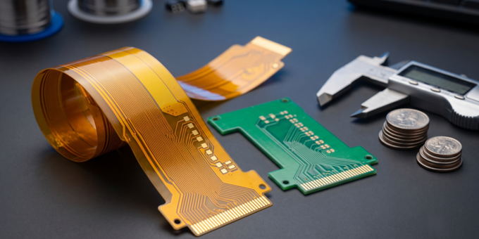
A catalog FFC ribbon, on the other hand, is a straight, uniform cable purchased based on pitch and the number of conductors. A custom flexible cable can branch, bend in three directions, carry soldered components, and end in three different connector types at the same time.
How Etched Flex Circuits Work in Electronic Applications
A custom flex does two jobs at once: it carries signals like a PCB and acts as a mechanical member like a cable. That is why it replaces a connector, a cable, and a second connector, providing a continuous copper path.
Most designs terminate in a golden-finger tail that slides into a zero-insertion-force housing. For example, a Hirose FH12 connector (0.5 mm pitch, 500 mA per contact, 50 V AC) clamps onto a stiffened tail, with no mating connector soldered to the flex, eliminating two solder joints and several millimeters of stack height. Bond a stiffener under a component field, reflow parts onto it, and you have a rigid island joined to a bending arm.
Why Choose Custom Etched Flex Circuits for Electronic Designs
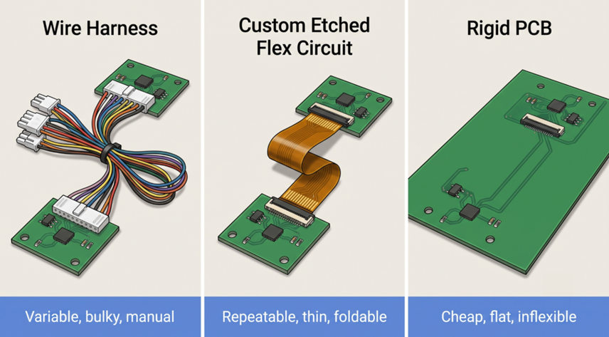
The honest answer is geometry. If your enclosure has a curve, a hinge, a stacked-board gap, or a moving lid, a flat board and a loom of discrete wires will fight the mechanics. The second reason is repeatability. Hand-dressed harnesses vary among operators, while fixed conductor positions enable controlled impedance and predictable crosstalk in a moving assembly.
- Fixed geometry: Identical trace routing and length on every board
- Fewer joints: One etched path replaces crimps, splices, and mating pairs
- Serviceability: A silkscreened flex is easier to debug than a taped bundle
Rule of thumb: more than four discrete wires between the same two boards means a flex circuit is worth quoting.
How Are Custom Etched Flex Circuits Manufactured?
Circuit Pattern Creation and Precision Etching Process
Custom flex fabrication is subtractive: you start with more copper than you need and remove the rest.
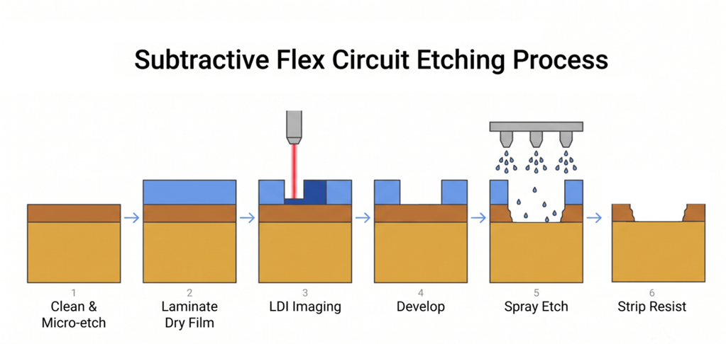
- Clean and micro-etch the flexible copper-clad laminate to strip oxide and oils so the resist will stick.
- Laminate dry film resist under heat and roller pressure across the whole panel.
- Imagine the pattern with laser direct imaging, which writes your artwork straight onto the resist with no physical phototool.
- Develop the resist so that the unexposed areas wash off, bearing the copper that must go.
- Spray etch the panel so the etchant clears the exposed copper down to the polyimide.
- Strip the resist, leaving only the finished conductor pattern.
The step engineers argue about is imaging, not etching. Polyimide is dimensionally live: it moves with humidity and shrinks once its copper restraint is etched away. A phototool cannot chase that movement, but laser direct imaging (LDI) scales artwork per panel to compensate.
Lamination, Coverlay, and Surface Finishing
When the copper pattern is created, it needs to be sealed. A coverlay is a laser-cut polyimide film with adhesive pre-coated on it, pressed in a heated hydraulic press so that only the pads are exposed. Since it is important that the adhesive fit between the traces but not squeeze into the pad openings, the aperture is drawn 0.1 mm (4 mil) larger than the pad on each side.
Exposed pads then receive a finish. ENIG at 1 to 2 microinches of gold is the flex default because it stays flat for fine-pitch reflow and survives the repeated insertions a ZIF tail sees. Stiffeners are bonded last, followed by profiling with a punch die or a UV laser.
Electrical Testing and Quality Inspection
Every custom flex should leave the factory electrically proven, not just visually approved: optical inspection for width and spacing defects, then 100% net testing by flying probe or fixture.
The difference between flexible and rigid QC is the mechanical qualification. Flexural endurance is measured according to IPC-TM-650 Method 2.4.3, the MIT fold test, which consists of a coupon being flexed around 175 double bends per minute and a cycle count until failure. Acceptance criteria are found in IPC-6013, which specifies Class 1, 2, and 3 performance levels. Bare-board net testing is not an indicator of bend life. If your product needs to be flexible in service, request specifically flex-cycle data on your stack-up and not only a material datasheet number.
Materials Used in Custom Etched Flex Circuits
Polyimide Substrate for Flexible Circuit Reliability
The material that almost all engineers still refer to as Kapton is actually polyimide film and is the base material used for almost all custom etched flex circuits. It withstands lead-free reflow and is resistant to solvents, while maintaining mechanical properties over a temperature range that polyester film can't even come close to.
The choice that actually changes reliability is adhesive versus adhesive-free construction. Laminates governed by IPC-4204 come in both forms.
| Construction | Example Material | Service Temperature | Why It Matters |
| Adhesive-based (3-layer) | DuPont Pyralux LF (copper, acrylic, polyimide) | Around 200 C | Lower cost, strong peel strength, but the acrylic layer swells in the Z-axis and can push on plated barrels during reflow |
| Adhesive-free (2-layer) | DuPont Pyralux AP (copper bonded directly to polyimide) | Around 300 C | Thinner build, better dimensional stability through multiple lamination cycles, and steadier loss tangent at high frequency |
Common dielectric thicknesses are 25 µm (1 mil) and 50 µm (2 mil). Thinner film bends more easily and lowers stack height; thicker film adds tear resistance and dielectric margin.
Copper Layers for Electrical Performance
The selection of the copper choice for a flex circuit is a grain-structure choice, not just a thickness choice. Copper is rolled into a rolled annealed (RA) state, which provides elongated grains in the foliar plane that are able to withstand repeated folding. Electrodeposited (ED) Cu is plated and has columnar grains that crack much earlier when subjected to cyclic strain.
Foil weight then sets your minimum feature size, because thicker copper needs more sideways etching time.
| Copper Weight | Foil Thickness | Typical Min Trace/Space | Best Use |
| 0.33 oz | 12 µm (0.5 mil) | 0.076/0.076 mm (3/3 mil) | Fine-pitch double-sided and 4-layer flex, camera, and display tails |
| 0.5 oz | 18 µm (0.7 mil) | 0.089/0.089 mm (3.5/3.5 mil) | General signal routing is the most common flex choice |
| 1 oz | 35 µm (1.4 mil) | 0.10/0.10 mm (4/4 mil) | Power rails, LED strings, motor, and battery interconnects |
You cannot have maximum current capacity and minimum trace pitch on the same layer, so split them: power on a 1 oz layer, signals on 0.33 oz.
Coverlay and Stiffener Options for Different Applications
Coverlay materials are specified under IPC-4203. Color is a real design choice: yellow is the standard low-cost film, black hides internal traces in a visible assembly, white reflects light under an LED, and transparent lets you inspect the copper after build.
Stiffeners add local rigidity where the flex must not flex, and mixing several types on one part is normal.
| Stiffener Type | Typical Thickness Range | What It Is For |
| Polyimide | 0.10 to 0.25 mm (4 to 10 mil) | ZIF tails, matching a connector's clamp thickness |
| FR4 | 0.10 to 1.6 mm (4 to 63 mil) | Component islands, screw-down mounting bosses, heavy connectors |
| Stainless steel | 0.10 to 0.30 mm (4 to 12 mil) | Thin, very stiff supports where FR4 is too bulky |
| PSA tape (3M 9077, tesa 8854, 3M 468) | 0.05 to 0.13 mm (2 to 5 mil) | Sticking the flex to a housing wall or battery pack |
| EMI shielding film | 18 µm (0.7 mil) | Shielding a routed signal run without a metal can |
Key Design Considerations for Custom Etched Flex Circuits
Layer Count, Circuit Structure, and Design Complexity
The vast majority of custom etched flex circuits are either one, two, or four layers, and each additional layer comes at a cost in the form of bendability. The single-sided flex on 25 µm polyimide is approximately 0.07 mm (2.8 mil) thick and can be folded like paper. A 4-layer at 0.20 to 0.45 mm is a routing solution, not a bending solution.
Structure inside the bend zone matters more than layer count alone:
- Hatch your ground planes in the bend region instead of pouring solid copper. A crosshatch keeps shielding while dramatically cutting bending stiffness and copper strain.
- Use a loose-leaf or air-gap build on multilayer flex, leaving the layers unbonded through the fold so each one bends on its own neutral axis.
Never place a via, plated hole, or component pad inside a bend zone. A drilled barrel is a stress riser, and the copper knuckle at its edge is where the crack starts.
Trace Width, Spacing, and Manufacturing Tolerance
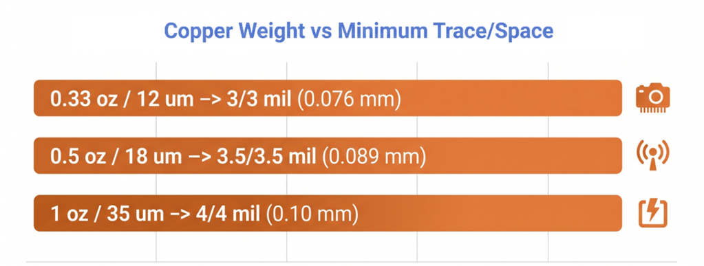
Design to the fab's real numbers rather than your EDA tool's defaults, and read the minimum trace and space off the copper weight you chose. Pushing that limit costs yield below Dimensional tolerances on flex are looser than rigid because the substrate moves. Plan for roughly ±0.1 mm (±4 mil) on profile dimensions and ±0.08 mm on hole diameters unless you have paid for a tighter class. Hold your critical dimension between two features on the same layer, pad center to pad center, rather than from a routed edge. Etched features track each other far better than they track the profile.
Bend Radius, Stiffener Selection, and Mechanical Requirements
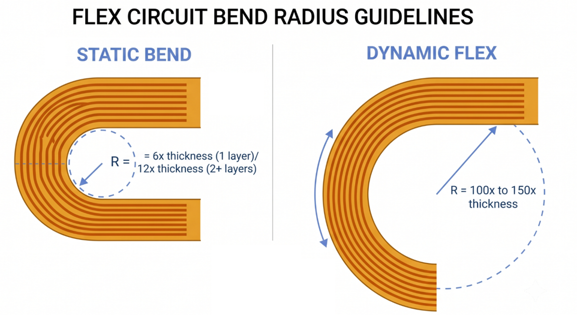
Bend radius is the number that decides whether your flex lives or dies. IPC-2223 gives multipliers of total flex thickness: 6x for single-layer static bends, 12x for multilayer static bends, and 100x for single-layer dynamic flexing, rising to 100x to 150x for multilayer dynamic use. Run the arithmetic before you commit to an enclosure. A 2-layer flex finishing at 0.20 mm needs a 2.4 mm (94 mil) static radius and a 20 mm dynamic radius, and a 20 to 30% safety margin pushes the dynamic figure past 25 mm. If your housing offers 8 mm, the mechanical design has to change, not the flex.
Even experienced designers trip on the same three items:
Mistake 1: Routing traces diagonally across the fold line. A diagonal conductor sees bending and shear strain at once. To fix this: run every trace perpendicular to the bend axis, with curved transitions into the bend.
Mistake 2: Ending a stiffener exactly at the bend line. The edge concentrates all the strain into one narrow band of copper. To fix this: set the stiffener back at least 0.5 mm (20 mil) from where bending begins.
Mistake 3: Stacking traces on top of each other on a 2-layer bend. Aligned copper multiplies stiffness and moves the neutral axis into a conductor. To fix this: stagger top and bottom traces so they interleave.
Advantages and Applications of Custom Etched Flex Circuits
Lightweight Design and Space-Saving Benefits
The weight saving is not marginal. A flex circuit replaces the conductor, the extruded insulation, the crimp terminals, the connector housings, and the cable ties with a film a fraction of a millimeter thick. Volume savings compound in a stacked assembly. Two boards joined by headers need 6 to 10 mm (236 to 394 mil) of dead space for connector bodies and mating depth, while a flex jumper folds into under 1 mm.
Reliable Performance for Dynamic Bending Applications
Reliability under motion needs rolled-annealed copper, a neutral axis that avoids conductors, and traces perpendicular to the fold, all three together. Miss one, and the flex looks fine on the bench and fails in the field. A wearable ECG patch came back from a field trial with intermittent dropouts after three weeks of wear.
The 0.5 oz copper showed hairline cracks where a trace crossed the fold diagonally on an electrodeposited, adhesive-based build. Respinning on rolled-annealed copper and adhesive-free polyimide, conductors turned perpendicular ended the failures. Custom flex also holds signal integrity while moving, because trace geometry and dielectric spacing stay fixed. That is what lets controlled-impedance display and camera tails run multi-gigabit lanes through a hinge.
Consumer Electronics, Medical, Automotive, and Industrial Applications
The reason for choosing flex differs sharply by sector.
- Consumer electronics: Folding phone hinges, laptop display cables, camera tails, and earbud cases. Dynamic bend life and stack height decide the build.
- Medical: Hearing aids, ECG and glucose patches, endoscope tips, ultrasound probes. Automotive: LED tail lamps, dashboard clusters, seat sensor mats, battery cell connection systems. Thermal cycling, vibration, and long service life.
- Industrial: Robot joint wiring, printer carriage cables, machine vision heads. Very high cycle counts, often millions of flexes.
Note: medical and automotive builds usually drive adhesive-free polyimide and Class 3 acceptance, a decision to make at the schematic stage, not at the quote stage.
Custom Etched Flex Circuits vs Traditional PCB Solutions
Flex Circuits vs Wire Harnesses
A wire harness wins on one axis only: no tooling and easy field changes, which keeps it ahead at very low volume. Everything else favors a custom-etched flex circuit once volume is reached. A flex is photographically identical on every unit, so routing variability drops out of your EMC results. It installs as one tail into a ZIF latch rather than a crimp, insert, dress, tie, and inspect sequence.
Flex Circuits vs Rigid PCBs
Neither technology replaces the other. Rigid FR4 is cheaper per square centimeter, supports far more layers, and mounts heavy components with no reinforcement.
- Choose rigid when the board sits flat in a box, needs many layers, or must dissipate real power.
- Choose custom flex when the circuit must fold, wrap a curve, bridge a hinge, or shed weight.
- Choose rigid-flex when you need both: rigid islands for components, flex arms for the interconnect, and no connectors between them.
The cost is compared at the assembly level, not the bare board level. Flex often loses on board price and wins once you count the connectors, cables, and labor it excludes.
Choosing a Custom Flex Circuit Manufacturer
Manufacturing Capability and Quality Control
Match their published limits against your worst feature, not your average one. Ask for minimum trace and space at your copper weight, supported layer counts, minimum via diameter, panel size, and profile tolerance.
Then check how they prove the board is good: 100% electrical net testing, AOI, and a stated IPC-6013 performance class. A supplier who cannot name their acceptance class is telling you something. A quoted minimum trace width means nothing without the copper weight attached to it. Three mil on 0.33 oz and three mil on 1 oz are not the same claim.
Material Options and Customization Support
A genuine custom flex shop offers choices, not a single recipe. Confirm they stock both laminate constructions, both copper grain types, more than one coverlay color, and a full range of stiffeners. Customization also means engineering conversation. You want a supplier who tells you your 0.15 mm (6 mil) bend radius is impossible on a 4-layer stack before they build it. Look for pre-production design review as a standard step, not a paid extra.
Prototype and Volume Production Capability
The jump from five pieces to five thousand is where most flex projects lose time. Confirm five things before you commit:
- Prototype lead time, and whether it is quoted online or by email.
- Whether prototype and production run the same line, laminate, and process window.
- Panel utilization feedback, since flex cost follows area yield more than part count.
- Assembly capability, if you need components soldered onto the flex.
- Whether stiffener and profile tooling carry over to volume.
JLCPCB's Custom Etched Flex Circuit Manufacturing Capabilities
Advanced LDI Technology for High-Precision Flex Circuit Fabrication
JLCPCB uses laser direct imaging for its flex lines; artwork is paid according to the number of panels,s and the registration is tight for double-sided imaging. That supports a minimum trace and space of 0.076 mm on 0.33 oz copper, 0.089 mm on 0.5 oz, and 0.10 mm on 1 oz. Builds run 1, 2, and 4 layers, with hole diameters from 0.1 to 6.5 mm held to ±0.08 mm, and panels up to 234 x 490 mm (9.2 x 19.3 in).
Adhesive-Free PI Material and Multiple Stiffener Options
The adhesive-free polyimide construction that has the best resistance to repeated lamination and bending is used as the standard substrate in 25 µm and 50 µm dielectric thicknesses. Finished builds range from 0.07 mm (single-layer) to 0.45 mm (4-layer stack).
All three copper weights, four coverlay colors, ENIG at 1 or 2 microinches, and 18 µm EMI shielding film can be specified around the core. Rigid component islands and ZIF tails can reside on the same part with stiffeners over them: PI, FR4, stainless steel, and PSA tapes.
Professional DFM Review and Flexible PCB Production Support
Each order is subjected to automated DFM before fabrication, which can identify spacing violations, holes that are too small, problems with coverlay openings, etc., and correct them at no cost. That makes flex iteration a design-week activity instead of a quarterly activity, when it only takes 4-5 days. Upload your Gerbers for an instant quote at JLCPCB's online quoting system, and if you need components reflowed onto the flex, pull them from the JLCPCB parts library.
Conclusion
Custom etched flex circuits reward designers who treat them as mechanical parts that happen to conduct. What determines whether the product survives is the bend-radius arithmetic, the choice of copper grain, the stiffener setback, and the decision to spend a little more on adhesive-free polyimide before anything is tooled. Get those four right and the technology repays you: fewer connectors, less mass, identical routing on every unit, and an interconnect that follows your enclosure instead of fighting it.

Frequently Asked Questions About Custom Etched Flex Circuits
What are custom etched flex circuits?
Custom etched flex circuits are made-to-order flexible printed circuits whose conductors are formed by chemically etching away unwanted copper from a polyimide-based laminate. Unlike a catalog FFC ribbon, every profile, bend zone, pad, and stiffener is designed for one product.
How are etched flex circuits manufactured?
The flow is subtractive. A flexible copper-clad laminate is cleaned, coated with dry-film resist, imaged by laser direct imaging, developed, and spray-etched so that only the desired copper remains. Coverlay lamination, surface finishing, stiffener bonding, testing, and profiling complete the part.
What materials are used in flexible circuits?
The core stack is polyimide film, copper foil, and an adhesive-coated polyimide coverlay. Copper is rolled annealed for bending or electrodeposited for static builds, in 12, 18, or 35 µm weights. Stiffeners of FR4, polyimide, steel, or PSA tape add local rigidity, and ENIG is the usual pad finish.
How can I get a custom flex circuit quote?
Export Gerbers, a drill file, and a fabrication drawing showing your layer stack, copper weight, coverlay openings, stiffener positions, and bend zones. Upload that package, select flex material and thickness, and you get pricing plus an automated DFM report in minutes.

Popular Articles
• Choosing the Right Bend Radius for Durable Flexible PCBs
• Flexible Meets Durable: Understanding Rigid-Flex PCB Technology
• PCB Stiffeners: An Essential Requirement for Flexible Circuits
• The Ultimate Guide to Flexible PCB: Types, Design, and Applications
• 45 Must-Know Flex PCB Design Tips You Can't Afford to Miss!
Keep Learning
Choosing the Right Bend Radius for Durable Flexible PCBs
Key Takeaways Mastering the bend radius is essential for reliable flexible PCB design. Following IPC-2223 guidelines, maintain a minimum of 6× total thickness for static bends and 100× for dynamic applications, while using thinner RA copper, adhesiveless polyimide, staggered traces, and cross-hatched patterns in flex zones. Proper material selection, layer stackup optimization, and adequate clearance from stiffeners can dramatically extend flex life and prevent premature trace cracking or delamination......
Flex PCB Stackup Design Guide: Layers, Materials & Reliability
Key Takeaways A reliable flex PCB starts with the right stackup design. The layer structure, material selection, and copper arrangement directly affect flexibility, bend life, electrical performance, and manufacturing reliability. This guide explains single-sided, double-sided, and multilayer flex PCB stackups, including polyimide materials, coverlay, copper types, and key design considerations for creating durable flexible circuits with JLCPCB. Did you ever wonder how a foldable phone can last for 20......
Flexible Meets Durable: Understanding Rigid-Flex PCB Technology
In the rapidly evolving world of electronics, the demand for smaller, more reliable, and more versatile devices continues to grow. To meet these demands, engineers and designers are increasingly turning to Rigid-Flex PCBs. The circuit boards combine rigid and flexible substrates into a single interconnected structure. This combination allows for complex designs that can bend and flex in specific areas while maintaining rigidity in others. To manufacture rigid flex PCBs, IPC offers advice and best prac......
PCB Stiffeners: An Essential Requirement for Flexible Circuits
A printed circuit board stiffener plays an important role when it comes to offering mechanical support to a PCB. They are particularly helpful for flexible circuit boards, that given their name, are flexible and in need of stiffness in certain places. Stiffeners are particularly required when components are placed in a flex zone & the weight of these components stresses the flex material. These components provide a rigid connection from the flexible portion to the solid board. This solidity makes appl......
The Ultimate Guide to Flexible PCB: Types, Design, and Applications
Key Takeaways JLCPCB 1–4 Layer Flex PCB: Supports 1 to 4-layer FPCs with polyimide (PI) substrates and trace/space down to 3/3 mil. Stiffener Selection: Use PI (0.1–0.25mm) for ZIF connectors, FR4 (0.1–1.6mm) for SMT support, and Stainless Steel (0.1–0.3mm) for high rigidity. Layout Optimization: Use cross-hatched copper ground planes and stagger 2-layer traces to eliminate the "I-Beam effect." Surface & Protection: Combine Immersion Gold (ENIG 1u"/2u") for SMT planarity with flex coverlay to protect ......
Medical Flex Circuits: Manufacturing, Applications, Materials, and Design Guide
Medical flex circuits made to fit inside a 1.0 mm disposable endoscope, wrap around a hearing aid shell, and sit on a patient's arm for ten straight days. When one fails, it is not a warranty return but a device history file and a regulatory conversation. In this guide, you will learn: What separates a medical flex circuit from a consumer one How they are built, tested, and released Polyimide, copper, coverlay, and stiffener choices Fine line, bend radius, and layer count limits What to check before c......