A Practical Guide to Circuit Design from Concept to PCB
16 min
- Circuit Design Fundamentals Every Engineer Should Know
- The Standard Circuit Design Workflow
- Turning a Circuit Schematic into a PCB Design
- Common Circuit Design Challenges and Practical Solutions
- From Circuit Design to Reliable PCB Manufacturing with JLCPCB
- FAQs about Circuit Design
- Conclusion
Key Takeaways
- Define clear circuit requirements and select suitable components based on electrical ratings, performance, and availability.
- Follow a structured design workflow from schematic capture and simulation to PCB layout and validation.
- Optimize component placement, routing, power distribution, and signal integrity to improve circuit performance.
- Apply DFM guidelines and complete ERC/DRC checks to prevent design errors and ensure smooth PCB manufacturing.
- Choose appropriate PCB materials, layer stackups, and assembly options to meet circuit requirements with JLCPCB.
Circuit design is the process of converting a function (reading a sensor, driving a motor, etc.) into components and connections that reliably perform it. The outcome is a schematic and eventually a printed circuit board that can be fabricated and assembled. The lowest-cost fix on paper is an early decision – an end-of-life part, a pull-up, or a supply voltage. These are the most expensive after etching copper.
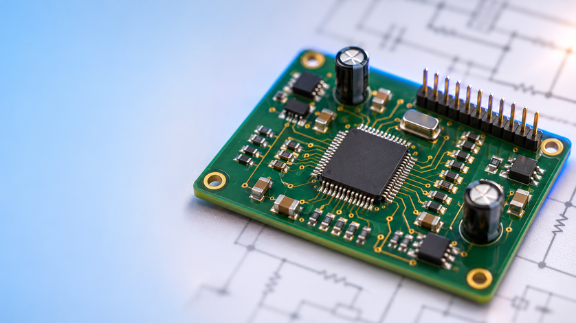
Figure 1: A circuit moving from schematic sheet to assembled PCB
This guide takes you through the typical process from requirements to schematic to layout and a working prototype. It also includes the most common issues that can cause a board to go back for a second revision.
Circuit Design Fundamentals Every Engineer Should Know
Each circuit is composed of a few common signal types and functions of components. If you know what type you are designing, you will know which rules are most important, since each type fails differently.
What Is Circuit Design?
Circuit design is the process of determining a circuit's functionality, selecting components to perform the desired function, and defining the interconnections required. It's in the middle between the product idea and the PCB layout. It outputs all the nets, part values, and part ratings, which are then passed directly into the layout and the bill of materials (BOM).
Schematic and PCB Layout are two different representations of the same circuit. On the schematic, a resistor is a shape connected to a net name; this represents a logical connection. So the same resistor is now represented as a footprint with copper pads, a trace width, spacing from other traces, and so on. Good circuit design is based on the premise of working in the first view and thinking in the second view. That is important because parasitic inductance, heat, and noise exist only when parts have positions.
Main Types of Electronic Circuits
The main types of circuits are analog, digital, and mixed-signal, and most real boards contain all three.
| Circuit Type | Signal | Typical Blocks | Main Design Concern |
|---|---|---|---|
| Analog | Continuous voltage or current | Amplifiers, filters, regulators, sensor front ends | Noise, offset, gain accuracy, stability |
| Digital | Discrete logic levels, usually clocked | Microcontrollers, logic, memory, interfaces | Timing, logic thresholds, edge rates |
| Mixed-signal | Both, converted at a boundary | ADCs, DACs, PLLs, comparators | Keeping digital noise out of analog paths |
Analog circuits respond to every millivolt, so their accuracy depends on component tolerance and on how much noise reaches them. Digital circuits tolerate noise up to a threshold and then fail abruptly. Mixed-signal circuits are harder than either. Digital switching draws transient current that travels through shared supply and ground connections into the analog side. Power circuits such as buck converters are, in principle, analog, but their high currents and fast edges make them the noisiest blocks on most boards.
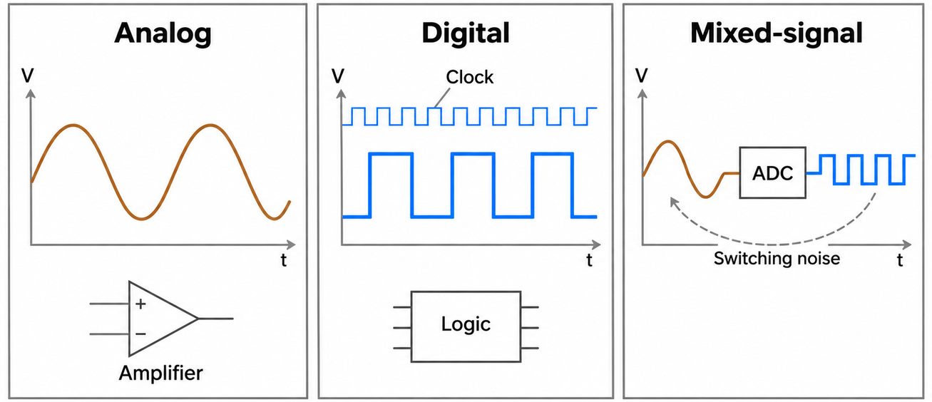
Figure 2: Analog, digital, and mixed-signal circuits and their signals
Essential Electronic Components and Their Functions
Electronic components are divided into passive parts, which store or dissipate energy, and active parts, which control or switch current.
| Component | Function in a Circuit | Key Selection Parameter |
|---|---|---|
| Resistor | Sets current, divides voltage, pulls inputs high or low | Value, tolerance, power rating |
| Capacitor | Stores charge, filters noise, decouples supply pins | Capacitance, voltage rating, dielectric (X7R, C0G) |
| Inductor | Stores energy in a magnetic field, filters, converts power | Inductance, saturation current, DC resistance |
| Diode | Passes current one way, rectifies, clamps transients | Forward voltage, reverse voltage, current rating |
| Transistor (BJT, MOSFET) | Amplifies or switches a load | Voltage rating, on-resistance or gain, power dissipation |
| Integrated circuit | Combines a complete function in one package | Supply range, interfaces, package, lifecycle status |
The selection parameter matters as much as the function. A 0.1 µF capacitor rated for 16 V on a 5 V rail leaves margin, while the same value at 100 V costs more and takes a larger package for no benefit. Ceramic capacitors with X7R or similar Class II dielectrics also lose capacitance under DC bias, so check the manufacturer's bias curve.
The Standard Circuit Design Workflow
The standard design workflow progresses from requirements to concept, schematic, and validation, with each step narrowing the choices for the next. It is iterative, so a failed test sends you back to the schematic rather than straight to a new layout.
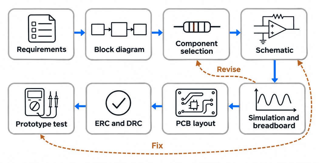
Figure 3: The standard circuit design workflow from requirements to tested board
Define Requirements and Develop the Circuit Concept
Requirements are numbers, not wishes. Record the supply range, peak and standby current, all signals and voltage levels, operating temperature, board size, and interfaces. The input range is defined by a requirement like "runs from a single-cell lithium battery" (3.0 V to 4.2 V). With this range determined, it determines whether a linear regulator, a buck converter, or a buck-boost converter is the appropriate supply.
The idea is to convert these numbers into a block diagram. Each block, including the power block, processing block, sensing block, protection block, etc., has its own input/output and power budget. This way, each block can be designed and tested separately, and faults remain local. The diagram depicts the analog/digital interface, too, and that's where most of the integration bugs later occur.
Select Components and Create the Schematic
When choosing the components, begin with the absolute maximum ratings and recommended operating conditions found in the datasheet, NOT the specification. Typically, parts are derated considerably below their ratings, such as a resistor operating at only half its specified power. Also, look at the lifecycle status, as a part that is 'not recommended for new designs' means a redesign later.
The schematic documents all choices. Draw it using functional blocks corresponding to the block diagram, name the nets, and do not use long wires. Each IC's decoupling capacitors should be placed near their symbols; they will be carried into the layout at the proper locations. Datasheet application circuits are best when starting regulators and interface chips, as the manufacturer has tested the values.
It's all about the details when it comes to starting the board. Tie unused CMOS inputs high or low, as TI's application report on floating inputs indicates that they may drift between the thresholds, oscillate, and consume additional current.
Simulate, Test, and Validate Circuit Performance
Simulation simulates a circuit's behavior before purchase of any part. A SPICE simulation of an amplifier, filter, or regulator loop displays gain, phase margin, transient response, and reruns in seconds when the value changes. A simulation includes only the parasitics that you include, and trace inductance, layout coupling, and real tolerances are not always included.
So check hardware critical blocks, too. A breadboard/evaluation board is used to verify a sensor interface or power stage in actual use, and a prototype PCB verifies the entire design. Write each test as a requirement (e.g., ripple below a set value), so that a pass or a fail is a number, not an impression.
Turning a Circuit Schematic into a PCB Design
Layout assigns each symbol a physical location, size, and copper connections. The schematic is the source of truth, and the layout tool verifies the board against it.
From Schematic Capture to PCB Layout
The netlist is used for the handoff between schematic and layout. A footprint is a copper pad pattern of the actual part that each symbol represents. The netlist then passes all connections to the layout tool, where unrouted connections are shown as thin rat's-nest lines. If the footprint is wrong, it is an expensive error since it only becomes apparent at assembly. IPC's current land pattern guideline (IPC-7352) is used; if available, the land pattern provided in the datasheet is used.
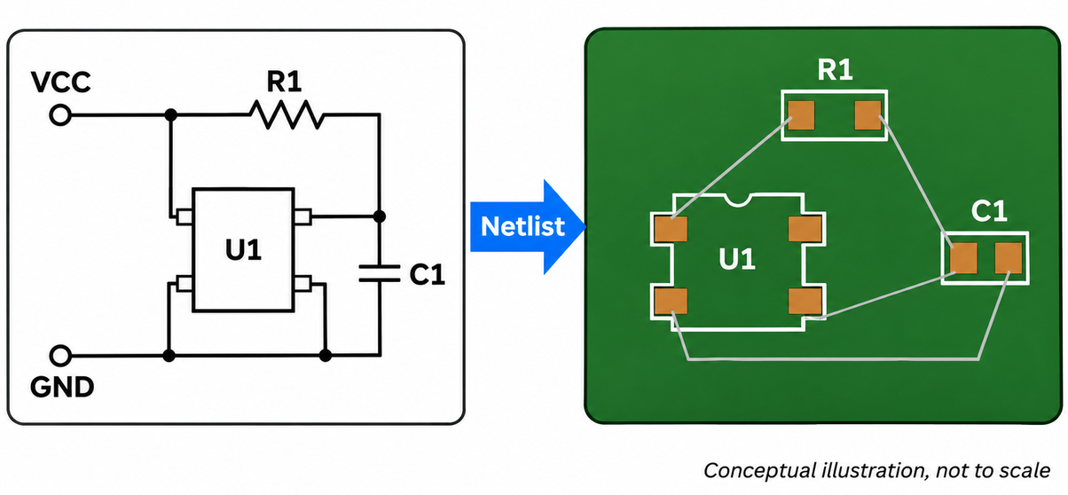
Figure 4: Schematic symbols become footprints connected by ratsnest lines
Set the board outline, layer stackup, and design rules according to the limits published by your fabricator before placing parts. The two views are largely synchronized, so a change to the schematic is reflected in the layout, and a connection in the layout that is not in the netlist is identified.
Component Placement and Routing Strategies
Placement decides most of the board's performance before a trace is routed. Start with parts whose positions are fixed: connectors, switches, mounting holes, and anything tied to the enclosure. Then place each functional block as a group. Keep the analog front end away from switching regulators and clocks, and keep the power entry near its connector to prevent high currents from crossing the board.
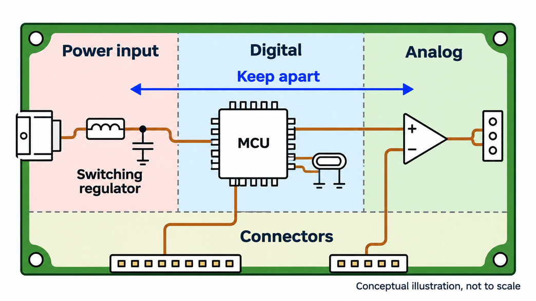
Figure 5: Placing circuit blocks by function on the board floor plan
Routing follows a priority order. Route power and ground first, as planes on a four-layer board or wide pours on two layers, since every other signal returns through them. Then route sensitive and high-speed signals, then everything else. Keep critical traces short with few layer changes, and size power traces for their current with a calculator based on IPC-2152. JLCPCB's placement and routing guidelines cover these rules in more detail.
Design Printed Circuit Boards for Manufacturability
To create printed circuit boards that build out without issue, keep all features within the fabricator's standard process. Avoid using minimum values unless required by a part. The width of the trace, spacing, drill size, annular ring, and solder mask clearance are all published limits, and a board drawn at standard values will be cheaper and yield better results. The generic printed board design standard IPC-2221 provides guidelines for conductor spacing.
Assembly performs some checking. Mount surface parts on one side wherever possible, include pick-and-place machine fiducials, and indicate polarity/pin 1 on the silkscreen. Test points on all supply rails and key signals should be left on. Then, create the Gerber, drill, BOM, and placement files in a single revision, and the fabricator and assembler will build exactly the board you checked.
Common Circuit Design Challenges and Practical Solutions
Most board revisions trace back to a few problems that start in the schematic and appear only in the layout or on the bench. Each has a known cause and a design-stage fix.
Power Supply and Signal Integrity Issues
Power problems usually come from the path between the supply and the IC, not from the regulator. A switching digital chip draws short current pulses that the trace inductance cannot deliver quickly enough, causing the local supply voltage to dip. A decoupling capacitor, typically 0.1 µF ceramic, at each supply pin with a short via to ground supplies that charge locally. A bulk capacitor of around 10 µF nearby handles slower load changes.
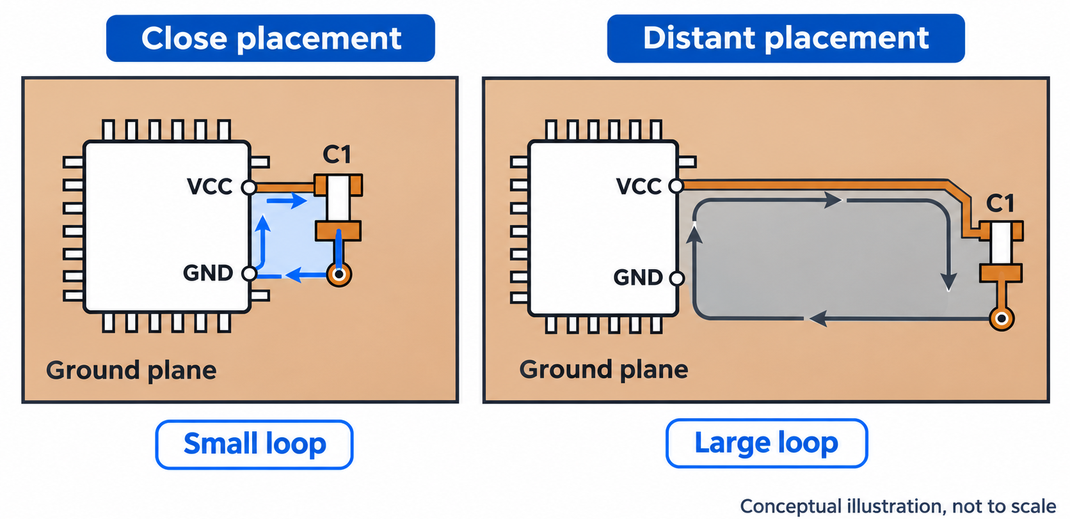
Figure 6: Decoupling capacitor placement and the current loop it creates
Signal integrity problems grow with edge rate rather than clock frequency. A fast edge on a long trace can reflect at an unterminated end and ring, so clocks and reset lines trigger falsely. Keep fast signals short and route them over a continuous ground plane. Add a series termination resistor near the driver on long traces, and use controlled impedance where interfaces such as USB or Ethernet require it.
Thermal Management and Electromagnetic Interference
The heat begins with a calculation in the schematic: A linear regulator dissipates the difference in voltage between the input and output multiplied by the load current. This means that at 0.3 A, 12 V will drop to 3.3 V, resulting in approximately 2.6 W of heat, which is too much to dissipate from a small package without a lot of copper, so a buck converter is generally a better choice. Parts requiring power dissipation should be copper-poured over the thermal pad; thermal vias should connect to inner planes; and electrolytic capacitors and precision references should be kept away.
Current loops and fast edges are sources of interference: the larger the loop area, the more it radiates. Thus, the hot loop of a buck converter (from input cap to switch to input cap again) should be as small as possible as dictated by the layout. A slot in the plane causes it to flow around, increasing the loop size, while the high-frequency return current flows on the plane directly below the trace. JLCPCB's EMC design guidelines include filtering, shielding, and grounding.
Component Compatibility and Design Rule Checks
Compatibility issues are concealed at the boundaries between components. A microcontroller operating at 3.3V may not be able to reach the high threshold of a 5V logic input. A 5V output to a 3.3V pin may exceed the pin's absolute maximum rating unless the pin is specified as tolerant. So verify all of the interfaces for voltage levels, thresholds, and drive strength, and insert a level shifter if the datasheets don't overlap.
Automated checks find what reading doesn't. Schematic checks for unconnected pins, shorted outputs, and nets with no driver (electrical rule checks). Spacing, width, and drill violations are checked in the layout by design rule checks (DRC). Complete both before all releases, and only waive them if there is an explanation for why it is safe to do so.
From Circuit Design to Reliable PCB Manufacturing with JLCPCB
A verified design still has to be built on a process that matches its requirements. That means the fabrication, assembly, and test choices follow from the type of circuit you designed.
PCB Fabrication for Different Circuit Requirements
Different circuits need different board constructions, and the choice belongs in the design because it sets the layout rules.
| Circuit Requirement | Board Construction | JLCPCB Option |
|---|---|---|
| Simple analog or low-speed digital | 2-layer FR-4 | Standard FR-4, 0.10 mm (4 mil) minimum trace and space |
| Microcontroller with fast interfaces | 4 or more layers with ground planes | 1 to 32 layers, impedance control at ±10% |
| High current power stages | Heavy outer copper | 2-layer outer copper up to 4.5 oz |
| High-power LEDs or heat-dense parts | Metal-core board | 1-layer aluminum or copper core |
| RF circuits | Low-loss laminate | 2-layer Rogers and PTFE boards |
JLCPCB's PCB capabilities page lists the full limits, including 0.09 mm (3.5 mil) minimum trace and space on multilayer boards. Set your layout rules from that page before routing, because a design that relies on an unavailable value has to be rerouted.
PCB Assembly and Component Sourcing
Sourcing belongs in the design stage, because an out-of-stock part stops the build of a finished layout. Check each BOM line at the assembler, prefer common packages where performance allows, and record an alternate for passive parts. JLCPCB's parts library shows real-time stock, and its assembly page lists more than 680,000 in-stock components.
The assembly service you choose sets limits the layout must respect. JLCPCB's Economic PCBA places parts on one side, down to 0402, for 2 to 50 boards, while Standard PCBA places parts on both sides, down to 01005, for up to 80,000 boards. Assembled boards are checked with AOI, and X-ray is used for BGA, QFN, and LGA joints hidden under the package. Upload your Gerber, BOM, and placement files to get an instant quote.
Prototyping, Testing, and Production
Bring up a prototype in a fixed order, so each step relies only on what has already passed. Inspect the board, power it from a current-limited supply, and check each rail before connecting loads or loading firmware. Then test each block against its requirement in block-diagram order, because that isolates a fault to one section.
Production readiness asks whether every unit works at its temperature limits and in its enclosure. Fix what the prototype revealed in the schematic first, so the documentation matches the board, rerun the ERC and DRC, and only then release the next revision. A short functional test on the test points you placed turns bring-up into a repeatable check on every board.
FAQs about Circuit Design
Q: What are the steps of circuit design?
The steps are defining requirements, drawing a block diagram, selecting components, creating the schematic, simulating or prototyping critical blocks, laying out the PCB, running design rule checks, and testing the first boards. The process repeats whenever a test shows the design missing a requirement.
Q: What software is used for circuit design?
Most engineers use an EDA tool that combines schematic capture and PCB layout, such as KiCad, EasyEDA, or Altium Designer. SPICE-based simulators, often built into these tools, check analog behavior before layout. The right choice depends on board complexity, team workflow, and budget.
Q: What is the difference between a circuit diagram and a PCB layout?
A circuit diagram, or schematic, shows which components connect to which, using symbols and net names. A PCB layout shows where each part sits on the board and how copper traces, planes, and vias physically connect them.
Q: Can I design a circuit without simulation?
Yes, for many digital and low-speed circuits built from datasheet application circuits. Simulation becomes valuable for analog filters, amplifiers, and control loops, where component values set stability and accuracy, and a hardware prototype still confirms the final result.
Q: How do I learn circuit design as a beginner?
Start by building small circuits, such as an LED driver, a voltage divider, or a regulator, and measuring them against calculations. Then draw their schematics in a free EDA tool, lay out a simple two-layer board, and order it to learn the full flow.
Conclusion
Circuit design succeeds when each stage is settled before the next begins: requirements as numbers, a schematic checked against datasheets, a layout set to the fabricator's limits, and a prototype tested against the requirements. The cheapest fix is the earliest one, so spend time on the schematic and placement, where a change costs minutes rather than a board revision.
When your design passes its electrical and design rule checks, order your PCBs from JLCPCB and bring up the first boards with the test points you designed in.
Popular Articles
• PCB Silkscreen: All You Need to Know
• The Comprehensive Guide to Circuit Symbols: Key to Understanding Electrical and Electronic Diagrams
• Understanding Electrical Schematics: A Comprehensive Guide
• PCB Board Design: A Step-by-Step Guide for Beginners
• Design Guidelines for PCB Using FR4 Substrates
Keep Learning
Single-Sided PCB Design: Combining Simplicity with Sophistication
Key Takeaways Single-sided PCBs offer a simple, cost-effective solution for many electronic applications. SMT and THT components require different mounting and soldering arrangements. Proper layer orientation, Gerber files, and design rules help ensure manufacturability. Aluminum PCBs require careful attention to insulation, component mounting, and silkscreen placement. A printed circuit board (PCB) provides mechanical support for electronic components and establishes the electrical connections requir......
A Practical Guide to Circuit Design from Concept to PCB
Key Takeaways Define clear circuit requirements and select suitable components based on electrical ratings, performance, and availability. Follow a structured design workflow from schematic capture and simulation to PCB layout and validation. Optimize component placement, routing, power distribution, and signal integrity to improve circuit performance. Apply DFM guidelines and complete ERC/DRC checks to prevent design errors and ensure smooth PCB manufacturing. Choose appropriate PCB materials, layer ......
PCB Silkscreen: All You Need to Know
Key Takeaways The PCB Silkscreen Guide demonstrates that a properly designed legend layer is essential to prevent assembly failures and ensure long-term hardware reliability. By mastering modern manufacturing methodologies like Direct Legend Printing (DLP) and aligning layouts with JLCPCB's strict DFM design rules—including the absolute 0.8 mm character height limit and the automated 0.15 mm silkscreen clipping protocol driven by solder mask precedence—engineers can seamlessly eliminate cold joints an......
The Comprehensive Guide to Circuit Symbols: Key to Understanding Electrical and Electronic Diagrams
Note Need a quick reference while reading schematics? Download our free, printable Circuit Symbols Cheat Sheet (PDF), featuring the most common IEC and ANSI symbols organized by category. Keep it on your desktop or print it for easy reference at your workbench. ⬇ Download the Free Circuit Symbols Cheat Sheet (PDF) Every electronic diagram is written in a visual language, and circuit symbols are its alphabet. From your first electrical schematic to a multi-layer board, knowing circuit symbols can make ......
Understanding Electrical Schematics: A Comprehensive Guide
Key Takeaways Schematics vs. Block Diagrams: Schematics detail exact components and connections; block diagrams only show high-level functions. Mark Polarity: Essential to prevent circuit failure and automated SMT placement errors at JLCPCB. Clean Layout: Use modular blocks and net labels (VIN, GND) to eliminate visual clutter. Manufacturing Ready: Follow DFM trace rules and export standard Gerber, BOM (LCSC C-IDs), and CPL files. Fast Troubleshooting: Isolate schematic blocks to test expected voltage......
PCB Board Design: A Step-by-Step Guide for Beginners
Key Takeaways This PCB Design Guide offers beginners a practical step-by-step approach to designing a compact 3A IP2312 lithium battery charger PCB — an upgraded alternative to the popular TP4056 module. It focuses on key techniques like schematic creation, optimized layout, proper trace routing for 3A current, and ground planes to build efficient and reliable boards. Printed Circuit Boards (PCBs) form the backbone of most modern electronic devices, providing a platform to connect electronic component......