Battery PCB Board: What You Need to Know
11 min
- What is a PCB board for a battery?
- Key Functions of a Battery PCB Board
- Benefits of a Battery PCB Board
- Types of PCB Designs Used in Battery Applications
- Key Design Considerations for Battery PCBs
- How Battery PCB Boards Are Made
- FAQ About Battery PCBs
- Conclusion
Key Takeaways
- Battery PCB boards support power distribution, protection, monitoring, and cell balancing.
- PCB types include single-layer, multilayer, flexible, and HDI designs.
- Current capacity, thermal management, and routing density are key design considerations.
- Reliable manufacturing depends on proper materials, fabrication, assembly, and testing.
Battery PCB boards are used in a wide range of battery-powered electronics, from smartphones and laptops to electric vehicles and energy storage systems. Depending on the application, a battery PCB can provide electrical connections and support protection, monitoring, power management, and cell balancing functions through dedicated components and circuits.
Because battery-powered products must handle both electrical and thermal demands within limited space, battery PCB design requires careful consideration of current capacity, heat dissipation, component placement, board structure, and manufacturing requirements.
What is a PCB board for a battery?
A battery PCB board (often functioning as a Protection Circuit Module / PCM or Battery Management System / BMS) is a specialized circuit board designed to connect a device's battery to its electronic system. Its primary function is to regulate power delivery, monitor cell status, and prevent hazardous conditions such as overcharging, over-discharging, and overheating. Without a dedicated battery PCB, modern rechargeable lithium-ion and LiFePO4 batteries cannot operate safely or reliably.
Battery PCBs are commonly found in rechargeable battery-powered products such as smartphones, laptops, portable electronics, electric vehicles, and energy storage systems. Their design must account for electrical load, thermal conditions, available space, component requirements, and the intended battery configuration.
Key Functions of a Battery PCB Board
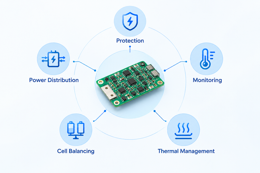
A battery PCB board provides the electrical infrastructure needed to connect a battery with the circuits and components it powers. Depending on the battery configuration and application, the PCB may support power distribution, battery protection, voltage and temperature monitoring, cell balancing, and thermal management. These functions are typically implemented through dedicated components and circuits mounted on the PCB rather than by the bare PCB itself.
Power Distribution
The PCB provides conductive paths for delivering electrical power from the battery to the connected circuits and loads. For battery applications with higher current requirements, the design needs to consider trace width, copper thickness, copper areas, connectors, and temperature rise to ensure that the power paths meet the application's requirements.
Battery Protection
Battery protection circuits can help protect rechargeable batteries against abnormal operating conditions such as overcharge and over-discharge. The PCB provides the electrical connections and layout needed to integrate protection components, such as protection ICs and MOSFETs, into the battery circuit.
Voltage and Temperature Monitoring
Battery-related PCBs can incorporate circuits for monitoring battery or individual cell voltage and temperature. Voltage monitoring helps detect conditions outside the required operating range, while temperature-sensing components can provide information for thermal protection and control.
Thermal Management
Power components and charging circuits can generate heat during operation. A well-designed PCB can help manage this heat through appropriate copper areas, component placement, thermal vias, and suitable PCB materials. The specific thermal design depends on the power level, component characteristics, and mechanical environment of the product.
Cell Balancing
In battery packs containing multiple cells, balancing circuits can help maintain appropriate voltage levels between cells. However, cell balancing is not required for every battery PCB; whether it is needed depends on the battery architecture and the functions implemented by the battery management or protection circuit.
Summary Table
| Function | What the PCB Supports | Key Design Considerations |
|---|---|---|
| Power Distribution | Provides conductive paths between the battery and connected loads | Trace width, copper thickness, current, temperature rise |
| Battery Protection | Integrates protection circuits for abnormal battery conditions | Protection ICs, MOSFETs, current paths |
| Voltage Monitoring | Provides connections for monitoring battery or cell voltage | Sensing traces, circuit layout, signal integrity |
| Temperature Monitoring | Integrates temperature-sensing components and related circuits | Sensor placement, heat sources, thermal conditions |
| Thermal Management | Helps distribute and dissipate heat generated by components | Copper area, thermal vias, component placement, PCB material |
| Cell Balancing | Supports balancing circuits in multi-cell battery packs | Cell configuration, balancing circuit, sensing connections |
Benefits of a Battery PCB Board
A well-designed battery PCB can help integrate electrical connections, protection circuits, monitoring functions, and power-management components within a compact board area. Key benefits include:
Reliable Power Delivery: Properly designed conductive paths help accommodate the electrical requirements of the battery and connected loads.
Improved Thermal Management: Appropriate copper areas, component placement, and suitable PCB structures can help manage heat generated by power components.
Compact Integration: Multilayer, flexible, or HDI PCB technologies can help integrate more circuitry into space-constrained products.
Manufacturing Consistency: A PCB designed according to defined manufacturing capabilities and design rules is easier to fabricate and assemble consistently.
Types of PCB Designs Used in Battery Applications
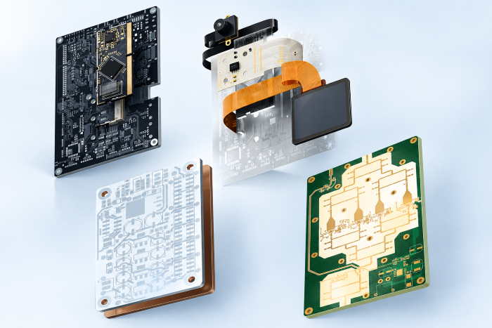
Battery PCB designs vary according to the electrical, mechanical, and space requirements of the final product. Layer count is one of the basic considerations, while flexible and HDI technologies can be selected when the product requires a different form factor or higher routing density.
Therefore, these PCB designs should not be viewed as completely separate categories. For example, a battery application may use a multilayer PCB, while an HDI structure can be applied when higher interconnection density is required. The most suitable approach depends on the circuit complexity, available space, current requirements, and mechanical structure of the product.
| PCB Design | Main Characteristics | Typical Application Considerations |
|---|---|---|
| Single-Layer PCB | Uses a single copper layer and has a relatively simple routing structure. | Suitable for simpler battery-related circuits with limited routing and component density requirements. |
| Multilayer PCB | Uses multiple copper layers to provide additional routing space and allow more complex circuit structures. | Suitable when power, control, sensing, and other circuits need to be integrated within a limited board area. |
| Flexible PCB (FPC) | Uses a flexible substrate and can bend or conform to the mechanical structure of the product. | Useful for compact products or applications where the circuit must fit around limited or irregular spaces. |
| HDI PCB | Uses high-density interconnection technologies such as microvias to increase routing density within a compact area. | Suitable for space-constrained products that require dense interconnections and compact PCB layouts. |
Key Design Considerations for Battery PCBs
Designing a PCB for battery-powered applications requires more than simply connecting the battery to other components. The PCB must accommodate power distribution, heat generation, component density, and electrical safety while maintaining reliable performance. The following factors should be considered during PCB design to ensure the board meets the requirements of the battery-powered system.
Current-Carrying Capacity
Battery PCBs may carry relatively high currents, particularly in power delivery and charging circuits. Trace width, copper thickness, copper areas, and the overall current path should be considered together to handle the required current while controlling temperature rise. For higher-current designs, wider traces, larger copper areas, and appropriate power planes can help reduce resistance and heat generation.
Thermal Management
Charging and power-management components can generate heat during operation, making thermal management an important part of battery PCB design. Copper areas, thermal vias, component placement, and suitable PCB materials can help distribute and dissipate heat. Components that generate significant heat should also be positioned with sufficient consideration for surrounding components and temperature-sensitive circuits.
Space and Routing Density
Battery-powered products often have limited internal space, especially in compact consumer electronics and portable devices. The PCB layout therefore needs to balance component placement, routing space, board size, and connection requirements. Multilayer PCBs can provide additional routing space, while flexible PCB and HDI technologies can help address space constraints and higher interconnection density when required.
Electrical Safety and Reliability
Battery-related circuits require careful consideration of electrical safety and long-term reliability. The PCB layout should provide appropriate isolation between different circuits and maintain reliable power and signal connections. Protection and monitoring components should be placed and routed appropriately so that voltage, temperature, and other battery-related parameters can be monitored effectively.
By considering current capacity, thermal performance, routing density, and electrical reliability together, designers can develop a battery PCB that meets both electrical and mechanical requirements. Material selection, layer structure, and manufacturing capabilities should also be considered early in the design process to ensure the final PCB can be manufactured reliably and consistently.
How Battery PCB Boards Are Made
The process of making a battery PCB board involves several steps:
⦁ Design: The first step is creating a design for the board. This design includes the layout of the circuits and ensures the PCB can handle the power requirements of the battery.
⦁ Material Choice: FR-4 is a common substrate for rigid battery PCBs because it provides a practical combination of mechanical strength, electrical insulation, and thermal performance. For applications with more demanding temperature requirements, higher-Tg FR-4 materials are also available. JLCPCB offers standard FR-4 as well as higher-Tg FR-4 options for multilayer boards.
⦁ Layering: For multilayer battery PCBs, cores, prepreg, and copper foil are arranged according to the required stackup. The stack is then laminated under controlled temperature, pressure, and vacuum conditions to form the multilayer structure. Copper patterns, drilling, plating, solder mask, and surface finishing are subsequently processed according to the PCB design and manufacturing requirements.
⦁ Assembly: Once the PCB is fabricated, components such as resistors, capacitors, power devices, and monitoring ICs can be assembled onto the board using SMT and/or through-hole assembly, depending on the design.
⦁ Testing: After assembly, battery-related PCBAs can undergo different inspection and testing processes depending on the product requirements. JLCPCB's SMT assembly quality-control system includes SPI for solder paste inspection, AOI for component placement and soldering inspection, and X-Ray inspection for hidden solder joints such as those under BGA, QFN, and LGA packages. Functional Circuit Testing (FCT) is also available as a customized SMT service option when functional verification is required.
Battery PCB Design Checklist
| Design Factor | What to Consider |
|---|---|
| Current | Required load current, trace width, copper thickness, and temperature rise |
| Thermal Management | Copper area, thermal vias, component placement, and heat dissipation path |
| Layer Count | Routing density, power distribution, sensing circuits, and board thickness |
| Material | FR-4, high-Tg FR-4, FPC, or metal-core options according to application |
| Space | Component size, routing density, connector position, and mechanical constraints |
| Manufacturing | Minimum trace/space, drill dimensions, copper distribution, and stackup |
| Assembly | Component package, SMT/through-hole requirements, and inspection requirements |
| Testing | Electrical, visual, AOI, X-Ray, or functional testing according to product needs |
FAQ About Battery PCBs
Q: What Is a Battery PCB Board?
A battery PCB board is a printed circuit board used to connect and support the electrical circuits associated with a battery-powered system. Depending on the application, it can support power distribution, battery protection, voltage and temperature monitoring, cell balancing, and thermal management.
Q: What Are the Main Functions of a Battery PCB?
The main functions of a battery PCB include distributing power, supporting battery protection circuits, monitoring voltage and temperature, managing heat, and supporting cell balancing in multi-cell battery systems. The specific functions depend on the battery configuration and application requirements.
Q: What Type of PCB Is Used for Battery Applications?
Battery applications can use single-layer, multilayer, flexible, or HDI PCBs depending on circuit complexity, available space, routing density, and mechanical requirements. Simpler circuits may use single-layer PCBs, while more complex or space-constrained designs may require multilayer, flexible, or HDI structures.
Q: What Should Be Considered When Designing a Battery PCB?
Key design considerations include current-carrying capacity, thermal management, space and routing density, and electrical safety and reliability. Trace width, copper thickness, component placement, thermal vias, layer structure, and electrical isolation should be considered according to the requirements of the battery-powered system.
Q:How Are Battery PCBs Manufactured?
Battery PCBs are typically manufactured through several stages, including PCB design, material selection, layer stackup and lamination, PCB fabrication, assembly, and inspection or testing. The manufacturing process and PCB structure should be selected according to the electrical, thermal, mechanical, and space requirements of the application.
Conclusion
Battery PCBs are an important part of many rechargeable electronic products, providing the electrical connections and circuit infrastructure needed for power delivery, protection, monitoring, and control. As battery-powered products become smaller and more integrated, PCB design must increasingly balance current capacity, thermal management, routing density, mechanical constraints, and manufacturability.
Choosing the appropriate PCB structure, materials, copper thickness, layer count, and assembly process can help create a reliable solution that meets the requirements of the final application. With rigid, flexible, multilayer, and HDI PCB manufacturing capabilities, JLCPCB provides options for battery-related PCB designs across different form factors and technical requirements.
Keep Learning
QFN Package: Structure, PCB Design, and Assembly
Key Takeaways Choose the correct PCB footprint: Follow the QFN manufacturer’s recommended land pattern and package datasheet. Optimize thermal management: Use appropriate thermal pads and thermal vias to improve heat transfer. Control solder paste application: Design stencil apertures to achieve suitable solder volume and reduce assembly defects. Inspect hidden solder joints: Use X-ray inspection when required by the product’s reliability needs and inspection plan. Design for manufacturability (DFM): ......
Navigating Automotive PCB Manufacturing Standards and High-Reliability Fabrication
Key Takeaways Harsh Operating Environments: Engineered to survive 15 years under thermal cycling (-40 °C to 150 °C) and severe vibration. Strict Compliance: Guided by IATF 16949, AEC-Q200 components, and IPC Class 3 standards. Targeted Materials: Leverages high-Tg/heavy copper for power and Rogers substrates for 77 GHz radar. Zero-Defect Inspection: Employs 3D AOI and X-ray testing to eliminate hidden solder joints failures. An automotive PCB has to keep working for fifteen years in the same place. Bo......
Battery PCB Board: What You Need to Know
Key Takeaways Battery PCB boards support power distribution, protection, monitoring, and cell balancing. PCB types include single-layer, multilayer, flexible, and HDI designs. Current capacity, thermal management, and routing density are key design considerations. Reliable manufacturing depends on proper materials, fabrication, assembly, and testing. Battery PCB boards are used in a wide range of battery-powered electronics, from smartphones and laptops to electric vehicles and energy storage systems.......
Medical PCB Manufacturing: Key Standards, Types, and High-Reliability Fabrication
Key Takeaways Strict Compliance: Demands ISO 13485 QMS certification, IPC Class 3 specs (25 µm copper barrels), and IEC 60601-1 safety rules. Targeted Substrates: High-Tg FR-4 handles autoclave heat, polyimide flex serves wearables, and metal/ceramic cores manage high power. Quality & Traceability: Layered AOI, X-ray inspection, and full IPC-1782 lot tracking prevent critical field failures. A medical PCB carries a level of responsibility that consumer electronics rarely face, because a patient’s diag......
A Complete Guide to Package Substrates: Materials, Structure, Types, and PCB Differences
Key Takeaways Definition: A package substrate is the fine-pitch organic carrier connecting a bare die to the system board. Not a PCB: Substrates are routed several times finer than advanced HDI and use entirely different dielectrics. Materials: BT resin cores carry wire-bond and CSP work, while glass-free ABF build-up film carries flip chip. Process: Semi-additive plating, not etching, is what makes single-digit micrometer lines possible. Constraint: Substrate capacity, not wafer supply, now limits hi......
Comprehensive Guide to QFN Packages: Advantages, Types, and Applications in Electronics
Key Takeaways Thermal Vias: Place 0.3mm vias in the exposed pad to draw heat away from the IC. Voiding Control: Apply a window-pane stencil (50–75% coverage) to prevent solder voids. Prevent Wicking: Use tented vias or Via-in-Pad to stop solder from leaking. Hidden Joints: Require X-ray inspection (AXI) since QFN leads are under the package. JLCPCB SMT: Fully supports 0.4mm pitch QFNs, Via-in-Pad, and AXI quality checks. Quad flat no-lead (QFN) packages are a type of IC package that are small, lightwe......