A Complete Guide to Package Substrates: Materials, Structure, Types, and PCB Differences
16 min
- What Is a Package Substrate?
- Package Substrate vs. PCB: Key Differences
- Package Substrate Materials: BT Resin, ABF, and Ceramic
- Package Substrate Structure
- Package Substrate Manufacturing
- Package Substrate Design Rules
- Wire-Bond vs. Flip-Chip Package Substrates
- Package Substrate Types
- Advanced Package Substrates
- Conclusion
- FAQs About Package Substrates
Key Takeaways
- Definition: A package substrate is the fine-pitch organic carrier connecting a bare die to the system board.
- Not a PCB: Substrates are routed several times finer than advanced HDI and use entirely different dielectrics.
- Materials: BT resin cores carry wire-bond and CSP work, while glass-free ABF build-up film carries flip chip.
- Process: Semi-additive plating, not etching, is what makes single-digit micrometer lines possible.
- Constraint: Substrate capacity, not wafer supply, now limits high-end AI package output.
A package substrate sits inside the chip package, so you never see it on the schematic. But it plays a major role in enabling high-pin-count processors. The die uses very fine-pitch connections, while the solder balls underneath the package are much larger and farther apart. The substrate fans out those signals, mechanically supports the package, and survives repeated reflow cycles.
In this guide, you will learn:
- How a package substrate differs from a PCB, layer by layer
- Why BT resin and ABF replace FR-4 inside the package
- Core, build-up, and coreless construction, and what each one costs you
- How fine the line and space rules get, and how they are plated
- Where the substrate-like PCB stops and the IC substrate begins
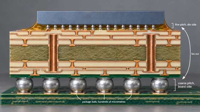
Figure: Flip-chip package cross-section showing signals fanning out from fine-pitch bumps to larger solder balls.
What Is a Package Substrate?
A package substrate is the multilayer carrier between the bare silicon die and the PCB. It connects the tiny pads on the die to the much larger solder balls underneath the package.
What Does a Package Substrate Do?
It has three main jobs:
- Electrical fan-out: spreads very fine die connections out to a wider BGA pitch.
- Mechanical support: provides the thin, fragile silicon die with a strong base.
- Heat spreading: uses internal copper to move heat away from the die.
For example, a die may use pads around 100 µm apart, while the package may use 0.8 mm solder-ball pitch. The substrate bridges that large difference. It does not process signals or perform calculations. Its job is simply to connect two very different scales. That same idea sits behind BGA, CSP, and flip-chip package designs.
Package Substrate vs. Semiconductor Substrate
- In wafer fabrication, the substrate is the crystal on which the device is built, such as silicon, silicon carbide, or gallium nitride. It directly affects the device’s electrical and thermal performance.
- In IC packaging, the substrate is the organic carrier between the die and the PCB. It mainly provides wiring, fan-out, and mechanical support.
So when a datasheet mentions a substrate, check the context. It may mean the semiconductor crystal or the package laminate.
Package Substrate vs. PCB: Key Differences
A package substrate and a PCB both use copper and dielectric layers, but they are built at very different scales. Package substrates can use much finer plated traces, while standard PCBs rely on coarser etched features.
| Parameter | Package Substrate | Multilayer PCB | What It Changes for You |
|---|---|---|---|
| Minimum line/space | 10/10 µm by semi-additive plating, 7/7 µm in development | 0.09/0.09 mm (3.5/3.5 mil) minimum for multilayer boards at JLCPCB | Escape routing density under a fine-pitch part |
| Dielectric | ABF build-up film or BT resin | FR-4 epoxy and prepreg | Loss, moisture uptake, and laser drillability |
| Reinforcement | Glass-free in the build-up layers | Woven E-glass throughout | Whether a small laser via can be cut cleanly |
| Layer structure | Thin core with build-up tiers on each side, or coreless | 1 to 32 layers around a full-thickness core | Total package or board thickness |
| Via formation | Laser-drilled microvias, often stacked | Mechanically drilled holes, 0.15 mm (5.9 mil) minimum | Whether a via can sit inside a pad |
| Interconnect pitch served | Die bumps near 90 to 130 µm (3.5 to 5.1 mil) | Package balls at 0.4 mm (15.7 mil) and up | Which side of the package are you designing |
| Patterning process | Semi-additive: plate the copper you want | Subtractive: etch away the copper you do not want | The physical limit on line width |
Note
The substrate handles everything above the solder balls, while your PCB handles everything below them. The two meet at a land pattern you control, so that interface is where your effort belongs.
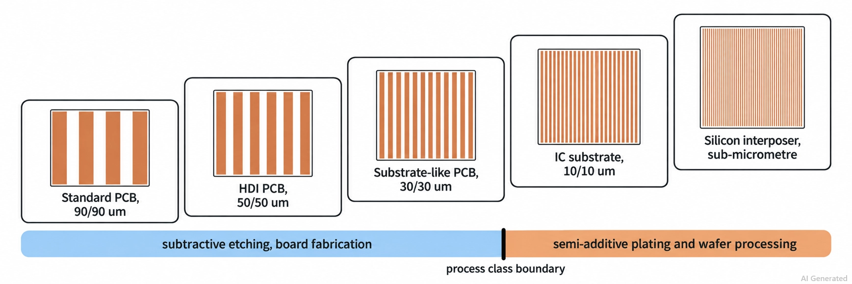
Figure: Interconnect density from standard PCB to HDI, IC substrate, and silicon interposer.
The JLCPCB manufacturing capabilities cited above come from its published capability data, while the 10/10 µm and 7/7 µm line/space figures come from Toppan’s FC-BGA specifications.
The difference is easy to see: 0.09 mm equals 90 µm, so a standard multilayer PCB trace is about nine times wider than a 10 µm package-substrate trace.
Package Substrate Materials: BT Resin, ABF, and Ceramic
| Material | Reinforcement | In-Plane CTE (ppm/°C) | Where It Is Used |
|---|---|---|---|
| FR-4 epoxy | Woven E-glass | 14 to 17 | System boards only, not package interiors |
| BT resin, MGC HL832 family | Woven glass with BT epoxy | 14 down to 3 by grade | Cores for CSP, BGA, and flip-chip substrates |
| ABF build-up film | None, glass-free | Low, grade-dependent | Build-up layers on flip-chip and FCBGA substrates |
| Ceramic, alumina, or AlN | Sintered ceramic body | About 7 | RF, high-power, and hermetic packages |
FR-4 is not well-suited for advanced package substrates. Its woven glass makes it very difficult to drill vias with a laser, and it expands much more than silicon when heated. FR-4 has an in-plane CTE of roughly 14–17 ppm/°C, compared with about 2.6 ppm/°C for silicon. That mismatch puts extra stress on the package connections during heating and cooling.
The closer a substrate sits to the silicon die, the more closely its thermal expansion should match that of silicon. Otherwise, heating and cooling put extra stress on the solder joints.
BT resin shows this clearly; Mitsubishi Gas Chemical lists grades around 14 ppm/°C for general BGA, CSP, and SiP use, while low-CTE flip-chip grades can drop to about 3 ppm/°C, much closer to silicon. That helps reduce stress under large dies.
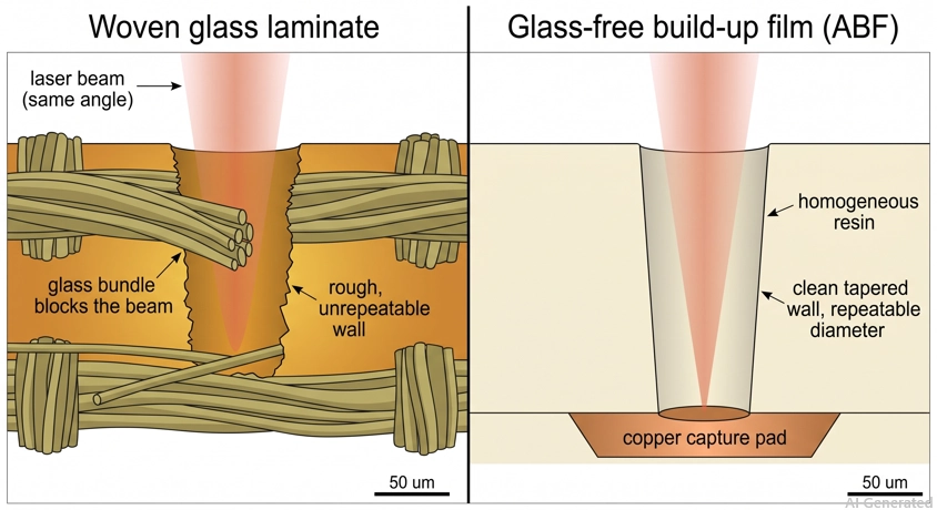
Figure: Glass-reinforced laminate beside glass-free build-up film, showing clean and ragged laser vias.
ABF (Ajinomoto Build-up Film) takes a different approach. It is a thin, glass-free insulating film with low thermal expansion and low dielectric loss. Because it has no woven glass, lasers can form very small and consistent microvias, which is why ABF is widely used in advanced processor substrates.
Package Substrate Structure
A thin, rigid core sits at the center of a substrate stack and carries plated through holes. Build-up layers are then laminated onto each face in turn, each one carrying its own laser microvias, until the required routing depth is reached.
Each element does one job:
- Core: A thin BT or glass-reinforced laminate that supplies stiffness and carries plated through holes between the two outer halves.
- Build-up layer: A laminated film, usually ABF, that adds one routing tier per side and hosts laser microvias to the layer beneath.
- Microvia: A laser-drilled hole, far smaller than any mechanical drill can make, often placed directly over the via below it.
- Solder resist: The patterned coating that defines pad openings and keeps solder off everything else.
- Surface finish: Typically ENEPIG or an organic coating, protecting pads for wire bonding, bumping, or ball attach.
The notation is the same one you already know from an HDI build-up stack-up. In a 2+4+2 substrate, the middle number counts the core layers, and each outer number counts the build-up tiers on that side. A 3+2+3 part, therefore, has three microvia tiers above and below a two-layer core, so it routes more but needs three lamination cycles per side instead of two.
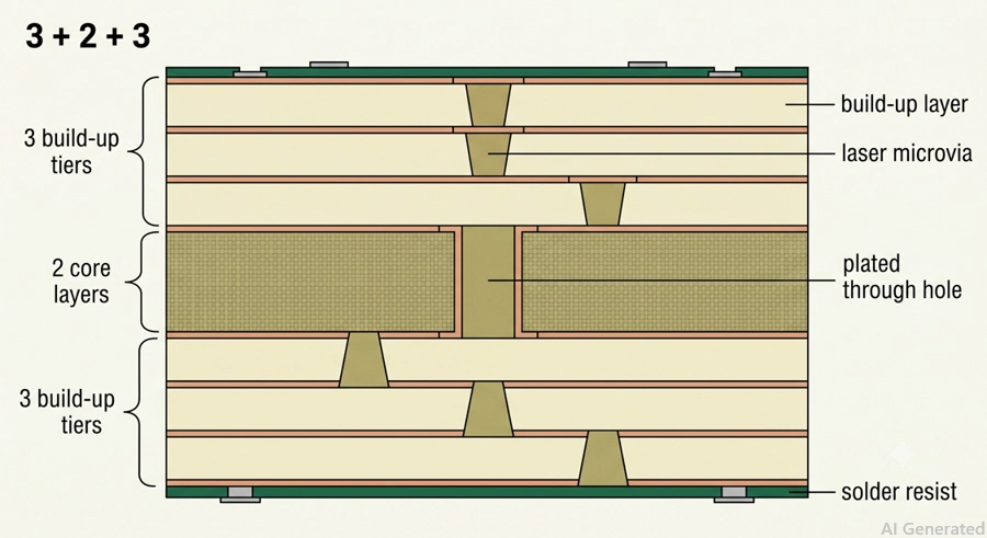
Figure: Build-up notation showing microvia tiers on each side of the substrate core.
Each added build-up layer needs another lamination, laser drilling, plating, and patterning step. That increases both cost and the chance of yield loss. Stacked microvias provide even greater routing density but add additional process complexity and cost.
Why Some Substrates Have No Core
What Is a Coreless Package Substrate?
Coreless substrates eliminate the core and its plated-through holes, and build every layer as a buildup film. Signals then run through short, stacked microvias instead of a long through-hole, so inductance drops and the finished package gets thinner.
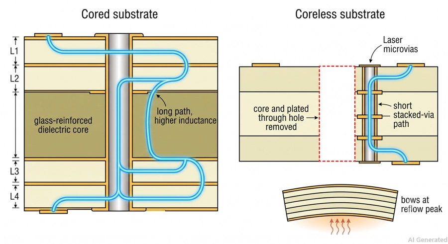
Figure: Cored and coreless substrates, showing the plated through hole removed in coreless construction.
The main trade-off is warpage. A rigid core helps keep the substrate flat, but a coreless design can bend more as it heats during reflow. If the package bows too much, corner solder balls can lift and lose contact.
Package Substrate Manufacturing
Very fine substrate traces are usually plated instead of etched. During etching, copper is removed from the sides as well as the top, which causes undercut and sloped trace walls. As the trace width drops below about 30 µm, that undercut becomes a much larger part of the line, making the process harder to control.
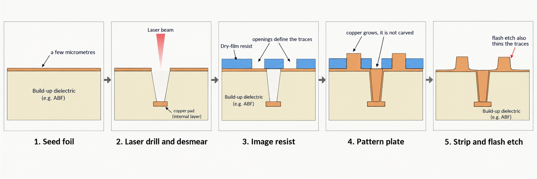
Figure: Modified semi-additive process from seed copper to pattern plating and flash etch.
The modified semi-additive process avoids that by starting with almost no copper, leaving almost nothing to undercut. The sequence runs:
- Laminate a very thin copper foil, on the order of a few micrometers, onto the build-up dielectric.
- Laser drill the microvias and desmear the holes.
- Imagine a dry-film resist in which the openings define exactly where copper will grow.
- Electroplate copper into those openings, building the traces upward instead of carving them out.
- Strip the resist, then flash etch away the thin seed foil between the traces.
The key difference between mSAP and full SAP is the seed layer.
In mSAP, the final flash etch removes the thin copper seed but also slightly thins the plated traces. A thicker seed needs more etching, which limits how fine the traces can be. Full SAP starts with an extremely thin electroless seed layer, enabling it to produce even finer features.
Package Substrate Design Rules
Substrate line and space capability is not one fixed number. It depends on the fabrication process used. The table below shows the range, from standard PCB manufacturing down to the much finer features used in advanced package substrates.
| Line/Space | Patterning Process | Where You See It |
|---|---|---|
| 0.09/0.09 mm (90/90 µm, 3.5/3.5 mil) | Subtractive etch | Multilayer PCB, JLCPCB minimum |
| 30/30 µm (1.2/1.2 mil) | Subtractive etch on thin foil | Substrate-like PCB and subtractive FC-BGA |
| 10/10 µm (0.4/0.4 mil) | Semi-additive plating | Production FC-BGA package substrate |
| 7/7 µm (0.3/0.3 mil) | Semi-additive plating | Next-generation FC-BGA, in development |
Each step down the ladder is a change of process, not a tighter version of the same one. If you need finer lines than one rung offers, you change equipment rather than tighten a tolerance.
Wire-Bond vs. Flip-Chip Package Substrates
The main difference is how the die connects to the substrate.
Wire bonding keeps the die face up and uses fine wires around its edges, while flip-chip packaging turns the die face down and connects it directly through an array of bumps.
See our guide to wire bonding vs. flip-chip packaging for a detailed comparison of these two interconnection methods.
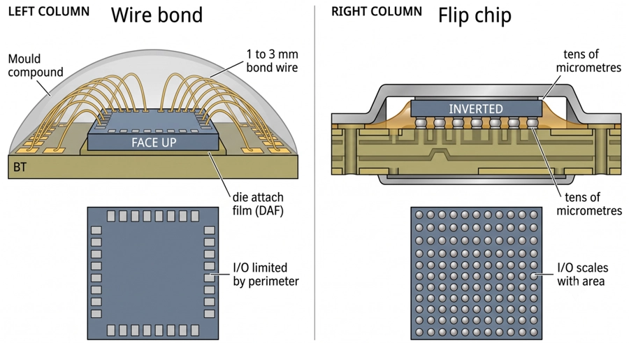
Figure: Same die with peripheral wire bonds and area-array flip-chip bumps.
- Pad location: Wire bonding uses a peripheral ring of pads, so the I/O count grows only with the die perimeter. Flip-chip uses the whole die face, so I/O grows with area and scales far further.
- Interconnect length: A bond wire runs one to several millimeters, while a flip-chip bump is tens of micrometers tall. Shorter paths mean lower inductance, which is why flip-chip dominates high-speed and high-current parts.
- I/O ceiling: Peripheral bonding runs out of room in the hundreds of pads. Area-array bumping can reach many thousands because it uses a two-dimensional grid instead of a line.
- Substrate demand: A wire-bond part can often be served by a 2- or 4-layer BT substrate with through-holes. A flip-chip part needs build-up tiers to escape the bump field, so layer count and cost rise sharply.
- Thermal path: An inverted die exposes its back face upward, so a lid or heat spreader can contact it directly. A face-up wire-bond die is covered by mold compound, which conducts poorly.
Note
Wire bonding remains cheaper and is still the right answer for low-I/O parts. Flip chip is what you buy when the pin count or the switching speed leaves no alternative.
Package Substrate Types
Most substrate-based packages fall into four main families. Their names usually combine the die-connection method with the package type, making part numbers easier to understand.
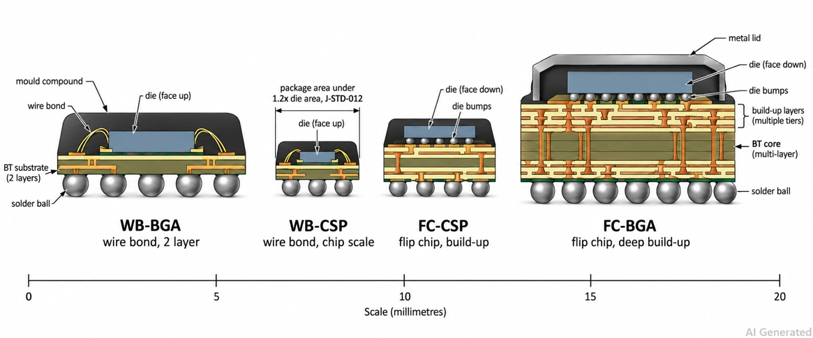
Figure: Four package families at the same scale, from wire-bond BGA to flip-chip BGA.
- Wire-Bond BGA (WB-BGA): A wire-bonded die on a 2 or 4 layer BT substrate with plated through holes, carrying solder balls at 0.5 mm (19.7 mil) pitch and up. It is the low-cost workhorse for microcontrollers and mid-range logic.
- Wire-Bond CSP (WB-CSP): A compact wire-bonded package designed to keep the package footprint close to the die size. J-STD-012 defines a chip-scale package as a single-die package that can be surface-mounted and has a package area no greater than 1.2 times the die area.
- Flip-Chip CSP (FC-CSP): A flipped die on a small build-up substrate, common in mobile application processors where both height and routing density are constrained.
- Flip-Chip BGA (FCBGA): A flipped die on a large multilayer build-up substrate, used for CPUs, GPUs, FPGAs, and AI accelerators. Toppan lists FC-BGA structures with up to 10 stacked vias, which shows how deep the build-up gets.
When selecting a package for a PCB design, our guide to BGA package types explains the key differences, applications, and PCB design considerations.
Advanced Package Substrates
High-end processors may require more connections than an organic substrate can directly handle. To increase density, designers place an additional carrier, such as a silicon interposer, between the die and the package substrate.
Silicon Interposers and 2.5D Packaging
A silicon interposer is a thin die with no transistors, carrying only wiring and through-silicon vias. It is fabricated using wafer processing rather than laminate processing, so its lines are sub-micrometers, whereas an organic buildup layer stops near 7 µm. That gap is why multiple dies that must exchange terabits per second sit on an interposer instead of directly on the substrate.
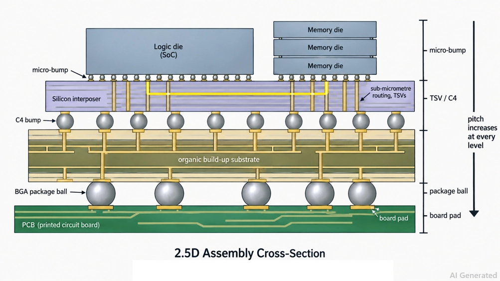
Figure: A 2.5D assembly stacking die, interposer, package substrate, and system board
The stack can have four levels: die, interposer, package substrate, and PCB. Each level spreads the connections to a wider pitch. In wafer-level packaging, that redistribution happens directly on the wafer, so no separate organic substrate is needed.
Glass Core Substrates
Glass has been proposed as a replacement for the organic core because its expansion coefficient is close to that of silicon, and it remains flat when heated. A flatter carrier at reflow means fewer open corner balls on very large packages, which is exactly the failure that limits how big an organic FC-BGA can get. Glass also supports finer through vias than mechanical drilling can produce in laminate.
A glass core helps reduce warpage, but it does not provide interposer-level wiring density on its own. That is why early glass-core packages still use conventional build-up layers around the core.
Why ABF Capacity Limits AI Chip Supply
High-end chip packaging is now limited partly by substrate capacity. Counterpoint Research estimates an ABF supply gap of about 10% in late 2026, rising to 20% in 2027. T-glass supply is also tight.
One reason is scale: an AI chip can use about 10 times more substrate material than a standard PC processor, while new substrate factories take years to reach full production. This does not directly affect normal PCB fabrication, but it can increase the lead time and availability risk for large, advanced FC-BGA components.
Conclusion
Package substrates bridge the gap between fine-pitch die connections and the larger features a PCB can handle. They also require different materials, equipment, and fabrication processes than standard PCB manufacturing. For most board designers, the substrate itself is not the part to design.
The real focus is the interface around it: land pattern, via-in-pad, fanout, stackup, and reflow process.
Package substrates may look like tiny PCBs, but they use different materials, finer features, and more advanced build-up processes. BT resin and ABF replace FR-4, while core, build-up, and coreless designs balance density, cost, and warpage. The key boundary is scale: once wiring moves beyond substrate-like PCB capability, the design enters true IC-substrate territory.
FAQs About Package Substrates
Q: What Is the Difference Between an IC Substrate and a PCB?
An IC substrate connects the bare die to the package solder balls. A PCB connects fully packaged components. IC substrates also use much finer traces than standard PCBs.
Q: What Is ABF and Why Is It Used in Package Substrates?
ABF (Ajinomoto Build-up Film) is a thin insulating material widely used in advanced package substrates. Its glass-free structure supports very small laser-drilled microvias.
Q: What Is a Coreless Package Substrate?
A coreless substrate has no rigid central core. It uses build-up layers and stacked microvias, making the package thinner but more sensitive to warpage.
Q: Is a Substrate-Like PCB the Same as an IC Substrate?
No. A substrate-like PCB (SLP) is still a PCB, but with finer features. An IC substrate sits inside the semiconductor package and uses even finer interconnects.
Keep Learning
Navigating Automotive PCB Manufacturing Standards and High-Reliability Fabrication
Key Takeaways Harsh Operating Environments: Engineered to survive 15 years under thermal cycling (-40 °C to 150 °C) and severe vibration. Strict Compliance: Guided by IATF 16949, AEC-Q200 components, and IPC Class 3 standards. Targeted Materials: Leverages high-Tg/heavy copper for power and Rogers substrates for 77 GHz radar. Zero-Defect Inspection: Employs 3D AOI and X-ray testing to eliminate hidden solder joints failures. An automotive PCB has to keep working for fifteen years in the same place. Bo......
Battery PCB Board: What You Need to Know
Key Takeaways Battery PCB boards support power distribution, protection, monitoring, and cell balancing. PCB types include single-layer, multilayer, flexible, and HDI designs. Current capacity, thermal management, and routing density are key design considerations. Reliable manufacturing depends on proper materials, fabrication, assembly, and testing. Battery PCB boards are used in a wide range of battery-powered electronics, from smartphones and laptops to electric vehicles and energy storage systems.......
Medical PCB Manufacturing: Key Standards, Types, and High-Reliability Fabrication
Key Takeaways Strict Compliance: Demands ISO 13485 QMS certification, IPC Class 3 specs (25 µm copper barrels), and IEC 60601-1 safety rules. Targeted Substrates: High-Tg FR-4 handles autoclave heat, polyimide flex serves wearables, and metal/ceramic cores manage high power. Quality & Traceability: Layered AOI, X-ray inspection, and full IPC-1782 lot tracking prevent critical field failures. A medical PCB carries a level of responsibility that consumer electronics rarely face, because a patient’s diag......
A Complete Guide to Package Substrates: Materials, Structure, Types, and PCB Differences
Key Takeaways Definition: A package substrate is the fine-pitch organic carrier connecting a bare die to the system board. Not a PCB: Substrates are routed several times finer than advanced HDI and use entirely different dielectrics. Materials: BT resin cores carry wire-bond and CSP work, while glass-free ABF build-up film carries flip chip. Process: Semi-additive plating, not etching, is what makes single-digit micrometer lines possible. Constraint: Substrate capacity, not wafer supply, now limits hi......
Comprehensive Guide to QFN Packages: Advantages, Types, and Applications in Electronics
Key Takeaways Thermal Vias: Place 0.3mm vias in the exposed pad to draw heat away from the IC. Voiding Control: Apply a window-pane stencil (50–75% coverage) to prevent solder voids. Prevent Wicking: Use tented vias or Via-in-Pad to stop solder from leaking. Hidden Joints: Require X-ray inspection (AXI) since QFN leads are under the package. JLCPCB SMT: Fully supports 0.4mm pitch QFNs, Via-in-Pad, and AXI quality checks. Quad flat no-lead (QFN) packages are a type of IC package that are small, lightwe......
Unlocking Smaller and Smarter PCBs with Embedded Components
Have you ever opened a smartwatch or a pair of wireless earbuds, looked at the miniature chip inside, and wondered how engineers could pack so much functionality into such a small enclosure? While surface-mount technology (SMT) has become incredibly sophisticated—with the advent of ultra-small 0201 and 01005 packages—there is a physical limit to how many components can be crammed onto the surface of a board. To bypass this bottleneck, the electronics manufacturing industry is increasingly turning to e......