Demystifying Bare PCB Quality for Reliability-Critical Applications
16 min
- Understanding the Essence of a Bare PCB
- Essential Production Quality Indicators for Unpopulated Boards
- The Crucial Role of Bare Board Testing
- How JLCPCB Ensures Zero-Defect Bare PCB Manufacturing
- FAQ about Bare PCB
- Conclusion
Key Takeaways
- Early Defect Catching: Catching faults at the bare board stage costs only the PCB, avoiding wasted components and rework later.
- Perfboard Risks: Zero PCBs lack reference planes and plated holes, causing signal noise above 10–20 MHz and pad lifting.
- Critical Material Specs: Reliability depends on hole barrel copper (20–25 µm), Tg, Td, and CTI ratings matching your operating environment.
- Finish & Shelf Life: HASL and ENIG last ~12 months, while OSP and Immersion Silver/Tin expire in ~6 months.
- Complete Inspection: AOI finds visible shape defects, while netlist-driven electrical testing verifies actual circuit connectivity.
A bare PCB is your last chance to catch a fabrication defect before it becomes an expensive assembly failure. Fixing a small fault at this stage may cost only the board. Once components are soldered, the same fault can waste parts, demand rework, and delay the build. This final fabrication checkpoint therefore, deserves your careful attention before component assembly begins. Copper thickness, laminate properties, surface finish, and electrical testing determine whether the finished board assembles correctly and keeps working throughout its service life.
In this guide, you will learn:
- What a bare PCB is, and where it sits between fabrication and assembly
- Why a zero PCB is not a substitute, and where it stops working
- Copper weight, laminate Tg, Td, and CTI, in numbers, you can check
- Surface finish thickness and shelf life, finish by finish
- How bare board testing finds opens and shorts that your eyes cannot
- What AOI catches, what electrical test catches, and what neither does
Understanding the Essence of a Bare PCB
Picture a city whose roads and junctions are finished before traffic arrives. A bare PCB is similar: its copper routes, holes, and protective coatings are complete, but no components carry current yet. The assembly adds those parts and activates the designed circuit.
What is a Bare PCB and Where Does It Fit in Product Development?
A bare PCB is the completed board before assembly adds any components. The factory has already built its conductive paths and protective layers; you or the assembly line supplies the parts later.
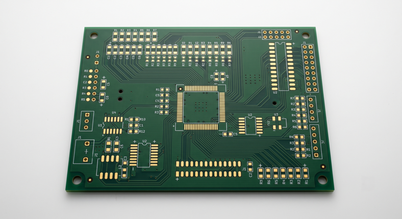
Strip one down, and you find six layers of work:
- The substrate, usually FR-4, woven glass cloth, is soaked in epoxy and cured hard
- Etched copper, on the outer faces and any buried inner layers
- Plated through holes, copper barrels carrying signals side to side
- Solder mask is the coating that keeps solder off everything but the pads
- Silkscreen, the white legend printing designators, and polarity marks
- A surface finish, a thin protective coating over the exposed copper
This handover marks the end of fabrication and the start of assembly, making it your last inexpensive checkpoint. A two-layer bare board can cost two dollars.
Bare Board vs. Zero PCB: Moving Beyond Perfboard Prototyping
A zero PCB is not a blank version of your design. It is a general-purpose board with no design in it at all: a grid of isolated holes on 2.54 mm (100 mil) pitch, each ringed by a copper pad. It is also called a perfboard or dot matrix board.
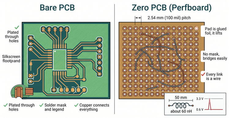
Three elements are missing, and each poses a practical issue:
- No plated through-holes: Copper foil is only bonded on one side of the pad. Repeat this process several times, and the adhesive may become softened, allowing the pad to come up with the part.
- No solder mask or silkscreen: Pads are bare, making it easier to bridge closely spaced joints; no markings mean there is no identification of parts or holes.
- No copper connections: All connections need to be made with wires, which have their own resistance, inductance, etc.
Let’s put on exact figures: A piece of wire, for example, 50 mm (2 inches) of 30 AWG wire has about 60 nH of inductance. That inductance can generate approximately 0.6 V of noise on the power rail if the current changes by 20 mA in 2 ns. That is a big blow to the logic margin on a 3.3 V board. If a PCB trace is laid over a ground plane, the inductance will be reduced to approximately 15-25 nH, and a power plane can further reduce the inductance to below 1 nH.
So a zero PCB stops being viable at four points:
- Above roughly 10 to 20 MHz, with no reference plane and no controlled impedance.
- Below 1.27 mm (50 mil) pitch, because the grid is fixed at 2.54 mm (100 mil).
- Above one or two amps, where current runs through a hand joint instead of a copper pour.
- Beyond one unit, because each takes hours and no two come out identical.
Stripboard, or Veroboard, sits in between. Continuous copper strips remove some wiring, and it still has no plated holes, no mask, and no plane. See our PCB design rules guide.
Essential Production Quality Indicators for Unpopulated Boards
Appearance alone cannot confirm bare-board quality. Two boards may look identical yet differ twofold in copper thickness, resin quality, or coating thickness, and each difference changes reliability throughout normal service.
Substrate Integrity, Copper Weight, and Layer Adhesion
Start with copper weight, the number most often misread. One ounce means one ounce of copper spread over one square foot, which is 35 microns (1.4 mil) thick. Half an ounce is 17.5 microns (0.7 mil), and two ounces is 70 microns (2.8 mil). On the outer layer,s the factory starts with thinner foil and plating brings it up, so "1 oz outer" is a finished thickness rather than a starting one. The number worth checking is the copper inside the hole: IPC-6012 asks for 20 microns (0.8 mil) average in the plated barrel for Class 2, and 25 microns (1 mil) for Class 3.
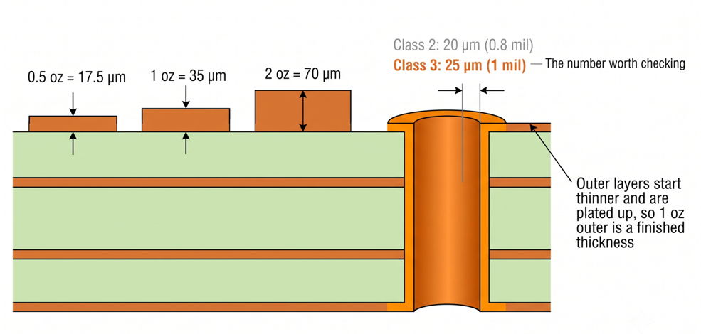
Three laminate numbers tell you what the substrate survives:
- Tg, the glass transition temperature: Above it, the resin softens and expands through the board thickness several times faster, which pulls the barrels apart. Standard FR-4 sits at 130 to 140 degrees C and high Tg at 170 to 180 degrees C. Keep your hottest operating temperature 20 to 30 degrees C below it, and see how to select the Tg of a PCB.
- Td, the decomposition temperature, is the temperature at which the resin has lost 5% of its mass. Lead-free reflow peaks near 245 to 260 degrees C, so ask for Td of 340 degrees C or better on boards facing two or three passes.
- CTI, the comparative tracking index: The voltage a surface survives against 50 drops of contaminated water before a carbon track burns across it. Standard FR-4 lands near 175 to 250 V, and high-CTI grades reach 600 V, so a low CTI forces wider creepage gaps on mains circuits.
Layer adhesion is where IPC-A-600 does its work. Measling is white spots where resin pulled away from the glass weave, crazing is the same, joined into lines, and delamination is a full separation seen as a blister. All three are judged by how far they close the gap between conductors. Tg tells you what the board survives in service, and Td tells you what it survives in the oven.
Solderability and Protective Surface Coating Uniformity
Exposed copper starts oxidizing immediately, and solder will not wet oxide reliably. A surface finish protects each pad by blocking oxygen. A judge who finishes by its thickness and, equally important, the uniformity of its coverage across the panel.
| Surface Finish | Typical Coating Thickness | Shelf Life | What a Thin or Uneven Coating Looks Like |
|---|---|---|---|
| HASL, leaded and lead-free | 2.5 to 7.5 microns leaded, 1.25 to 2.5 microns lead-free | About 12 months | Domed pads, so fine-pitch parts rock instead of sitting flat |
| ENIG | Nickel 3 to 6 microns (120 to 240 microinch), gold 0.05 to 0.125 microns (2 to 5 microinch) | 12 months or more | Pinholes in thin gold let the nickel below oxidize |
| OSP | About 0.2 to 0.5 microns (8 to 20 microinch) | Around 6 months | Invisible film, so failure shows as dull or pinkish copper |
| Immersion silver | 0.12 to 0.4 microns (5 to 16 microinch) | Around 6 months | Yellow or brown tarnish, worst near the board edges |
| Immersion tin | 1.0 micron (40 microinch) minimum, 1.15 to 1.3 typical | Around 6 months | Dull gray where copper-tin intermetallic ate the free tin |
Gold thicker than about 0.125 µm (5 microinch) can actually be a warning sign rather than an advantage. Too much gold can make the solder joint brittle, while the plating process can also attack the nickel underneath.
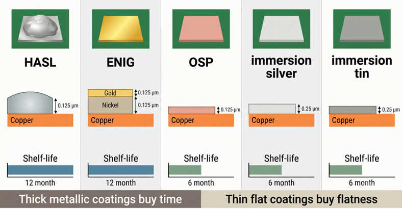
Thickness alone is not enough; coverage must also be uniform. Check pads across the panel, especially at the edges and center. A finish measuring 4 µm in the center but only 1 µm at the edge can pass an average reading while still causing assembly failures during solder paste printing and reflow.
The Crucial Role of Bare Board Testing
Bare board testing is the cheapest quality gate you will pass through. A defect caught here costs a board. Caught after assembly, it costs the board, the components, the placement time, and a slot in your schedule.
Eliminating Open and Short Circuits Prior to Component Placement
Bare board testing checks every design net in two complementary ways. Continuity confirms that intended connections exist. Isolation confirms that separate conductors remain electrically separate. Together, they expose hidden opens and shorts.
Those failures come from a short list of causes, and most are invisible:
- A copper sliver from under-etching, bridging two traces that should never meet.
- A scratch in the etch resist, thinning a trace until it opens.
- A void in a plated via barrel, so the copper tube inside the hole is not continuous.
- Drill breakout, where the drill wandered outside its pad.
- Inner layer misregistration, shifting a buried layer against the drilled holes.
The cost of catching a defect roughly multiplies by ten at each stage downstream, and the bare board is the earliest stage. A board that fails here is scrapped. The same board found at the final test takes your components and your delivery date with it.
Electrical Continuity Testing: Flying Probe vs. Automated Bed-of-Nails
Before choosing a machine, answer the important question: what reference does the tester use to judge your board?
The right answer is an IPC-D-356A netlist, a text file your CAD tool exports alongside the Gerbers. It names every net and gives the location, layer, hole size, and access of every pad on it. Send it, and the shop tests your copper against your schematic. Send Gerbers alone, and the shop extracts a netlist from the artwork instead, which finds etching and drilling faults but can never tell you the artwork was wrong. The older alternative is self-learning from a golden board: run a known-good first article through the tester and store its connections as the reference. The trap is obvious. If the golden board has a defect, every board afterward matches that defect and passes.
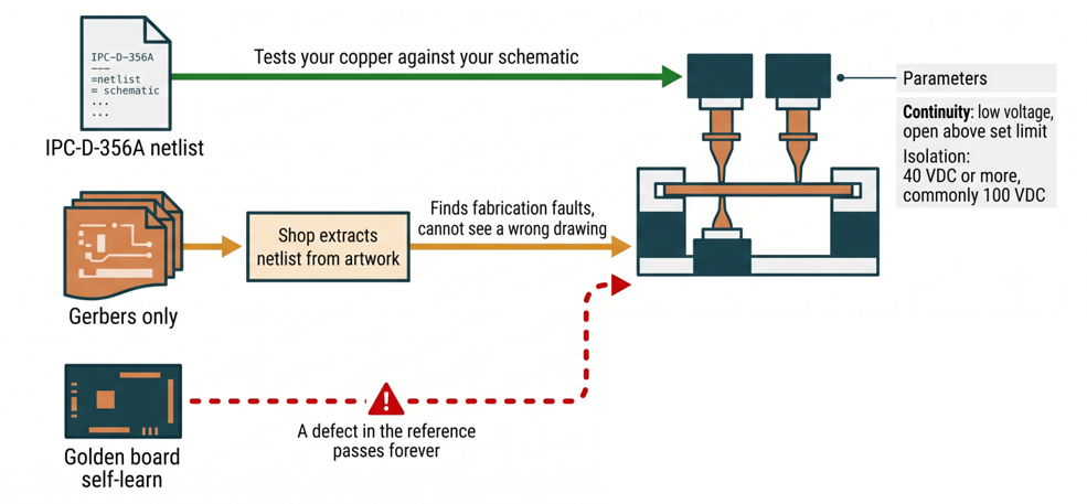
A dedicated fixture uses a separate spring probe for each test point on one specific board. A universal grid fixture uses a fixed bed of probes, typically from 2.54 mm (100 mil) down to about 0.64 mm (25 mil) pitch. A translator made from drilled plates then guides each probe to the actual pads on the PCB. The main difference is flexibility. With a universal fixture, only the translator plates change for each board. Both types make sense when the same PCB is tested repeatedly in production.
Electrical test cannot see:
- A barrel that conducts today but is 8 microns (0.3 mil) thick and will crack in reflow
- A trace necked to 60% of its drawn width, which passes continuity and still runs hot
- Solder mask misregistered onto a pad, or silkscreen ink printed across one
- Oxidation or contamination, so nothing about whether the solder will actually wet
- Controlled impedance, board thickness, warp, or outline dimensions
How JLCPCB Ensures Zero-Defect Bare PCB Manufacturing
AOI and electrical testing catch different bare-board defects. Automated optical inspection checks physical shape; electrical test checks connectivity. Omitting either one leaves an entire class of failures hidden until after component assembly begins.
High-Precision CNC Machining and Automated Optical Inspection (AOI)
Drilling accuracy makes everything downstream possible. Everything downstream is possible with drilling accuracy. JLCPCB is able to drill 0.15mm (6mil) diameter holes on 2-layer or higher boards, with a minimum finished via of 0.25mm (10mil), and they require at least 0.20mm (8mil) at 1 oz copper thickness for the hole annular ring; 0.25mm (10mil) is recommended. The collar of copper that remains around a hole after it has been drilled is the annular ring. Registration can wander by tens of microns across a panel, and a ring built to 0.05 mm (2 mil) may disappear on one side, and the connection hangs on a sliver.
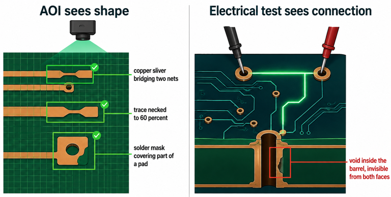
AOI, or automated optical inspection, photographs the etched copper and compares every image with CAM data using pixel-by-pixel comparison across each layer. It catches defects that have a visible shape: slivers, nicks, pinholes, missing copper, spacing violations, and solder mask shifted onto a pad. JLCPCB runs AOI after pattern plating and checks inner layers before lamination, the last stage when a buried defect remains accessible.
| Bare Board Defect | Found by AOI | Found by Electrical Test | What It Costs If It Ships |
|---|---|---|---|
| Coppersilver bridging two nets | Yes | Yes | A board that is dead the moment you power it |
| Trace necked to 60% of the drawn width | Yes | No | Runs hot, then opens in the field months later |
| Void inside a plated via barrel | No | Yes | An intermittent open nobody can locate |
| Solder mask covering part of a pad | Yes | No | An open joint that cannot be soldered |
| Oxidized or contaminated finish | No | No | Non-wetting across a whole panel at reflow |
100% Free Bare Board Testing for Enterprise-Grade Reliability
JLCPCB states that every board receives 100% AOI and electrical testing before shipment at no separate fabrication charge. Testing uses either flying probes or a bed-of-nails fixture. Both checks are included instead of being offered as optional line items. On a five-piece order of two-dollar boards, a test charge can represent much of the total, tempting buyers to decline it. The untested board can then consume a full day while you probe a circuit that was never at fault.
Check the remaining specification directly against your design. JLCPCB lists 1 to 32 layers on Grade A laminate from suppliers including Nan Ya, KB, and Shengyi. Trace and space start at 0.10 / 0.10 mm (4 / 4 mil) with 1 oz copper. Board thickness spans 0.4 to 4.5 mm (16 to 177 mil), with plus or minus 10% tolerance above 1.0 mm. Finish choices include HASL, lead-free HASL, ENIG, or OSP, and ENIG is required for 6-layer and RF builds.
Ready to Turn Your Design into a Finished Bare PCB?
Upload your Gerbers and your IPC-D-356 netlist together on the JLCPCB instant quote page, so the boards are tested against your schematic rather than your artwork. If you are assembling them too, check the JLCPCB parts library before finalizing footprints, and our guide to bare board quality control and testing covers the full inspection chain.
Specifically, Class 3 is not a checkbox that makes a board better. Against Class 2, it removes annular ring breakout entirely, where Class 2 tolerates up to 90 degrees of it behind a teardrop. It raises the average barrel copper from 20 microns (0.8 mil) to 25 microns (1 mil), and copper wrap onto the surface pad from 5 microns (0.2 mil) to 12 microns (0.47 mil). All three cost money and yield, so ask for Class 3 where downtime is unacceptable, not by default.
FAQ about Bare PCB
Q: What is a bare PCB?
A bare PCB is a finished circuit board with no components soldered to it. It has the substrate, etched copper, plated holes, solder mask, silkscreen, and a surface finish, and nothing else.
Q: Is a bare board the same thing as a zero PCB?
No. A bare board carries your specific design in etched copper. A zero PCB, also called a perfboard, is a general-purpose grid of isolated holes on 2.54 mm (100 mil) pitch with no circuit in it and no plated holes.
Q: Does bare board testing cost extra?
At JLCPCB, it does not. Every board gets 100% AOI and electrical testing, by flying probe or bed-of-nails, before shipping. Some suppliers do charge for it, so confirm before comparing quotes.
Q:How long can I store bare PCBs before assembling them?
It depends on the finish. HASL and ENIG typically hold about 12 months, while OSP, immersion silver, and immersion tin are usually rated around 6 months. Store them sealed with desiccant and count from the manufacturer's date.
Q: If a board passed the AOI and electrical test, is it guaranteed to be good?
No. AOI finds defects with a shape, and an electrical test finds defects with a resistance. Neither detects oxidation, contamination, or a finish aged past its shelf life, which is why storage and handling still matter.
Conclusion
A bare PCB looks like the simplest part of a build, which is why price often dominates its purchase. Yet the delivered board can differ from your specification in barrel copper, laminate Td, or surface-finish uniformity. None of those differences is obvious from across a workbench, although each one can shorten the board's life.
Judge bare-board quality by evidence you can check: copper weight, barrel-plating class, laminate Tg, Td, and CTI, finish thickness, manufacture date, and confirmation of electrical testing against your supplied netlist. Send that netlist with your Gerbers. Choose the finish for the date you will assemble, not the date you design. This timing protects solderability during storage. That keeps bare board testing at the stage where a defect still costs two dollars.

Popular Articles
• Understanding the Basics of Electronic Devices and Circuits
• Understanding Digital Circuit Timing: Setup Time, Hold Time, Contamination Delay & Clock Skew
• PCBs Explained: A Simple Guide to Printed Circuit Boards
• Guide to the Top 10 Commonly Used Electronic Components
• Digital 101: Fundamental Building Blocks of Digital Logic Design
Keep Learning
Polyimide Flex PCB: A Complete Guide for Engineers
A polyimide flex PCB can be folded about 285,000 times when the base film is 25 µm (1 mil) thick. Make that film 75 µm (3 mil), and the same MIT fold test gives up near 6,000 cycles. Bending is a strain problem, not a material problem. Copper sits above the center of the stack, so a bend forces it to stretch around the longer outer path. Figure 1: A polyimide flex circuit folded tight, with a stiffener holding the connector A thicker stack places the copper farther out, resulting in more stretch at th......
Flex PCB Bend Radius: Calculation, Minimum Radius & Design Guidelines
Flex PCB bend radius is the one dimension on an FPC that no design rule check will catch. Bend the circuit tighter than its material allows; the outer copper stretches from its elongation limit, and then it cracks. Figure 1: A flex circuit formed around a mandrel, with bend radius and stack thickness A flex circuit bends around a neutral axis near the middle of its stack. Copper below that line is squeezed, and copper above it is pulled. So the further a layer sits from the line, the harder it is to w......
Flexible Circuit Connector: Types, Features & Selection Guide
A flexible circuit connector clamps onto the bare copper at the end of a flex circuit, so nothing is soldered at that joint. The tail slides into the housing, and an actuator presses a row of spring contacts onto the pads. Every connector is built around one tail thickness. TE's 0.5 mm pitch 2328702 family expects 0.30 mm (12 mil) of flex, because the contact beams are deflected by exactly that dimension. Figure 1: Cross-section of a 0.5 mm pitch FPC connector with the tail inserted Feed it a bare sin......
FPC vs FFC: Understanding the Key Differences Between Flexible Circuit Technologies
The FPC vs FFC decision is really a question about how the copper was made. An FFC consists of flat copper strips laminated between two PET films. Every conductor runs straight from end to end at one fixed pitch, because nothing in that process can make a trace turn or branch. An FPC starts as copper-clad polyimide and is etched exactly like a rigid board. Traces can turn, taper, split onto a second layer, and land under a soldered component. The finished circuit can be as thin as 0.1 mm (4 mil). Figu......
A Comprehensive Guide to Capacitor ESR: What It Is, Good Values, and How to Measure It
Key Takeaways Definition: Capacitor ESR (equivalent series resistance) is the single resistance that represents the losses inside a real capacitor, from its electrodes, terminations, electrolyte, and dielectric. Why It Matters: Ripple current flowing through the ESR produces a ripple-voltage step on the supply rail and I²R heating in the capacitor, which limits the capacitor's ripple-current rating and service life. Conditions Matter: ESR varies with frequency, temperature, capacitance, case size, and......
Understanding IPC-6012 Standards for High-Reliability Rigid PCB Fabrication
Key Takeaways IPC-6012 vs. IPC-A-600: IPC-6012 is the binding specification, while IPC-A-600 is only for visual reference. Class 2 vs. Class 3: Class 3 requires thicker copper (25μm vs. 20μm) and zero plating voids. Coupon Verification: Quality is tested by microsectioning panel coupons after thermal stress. Upfront Callout: Specify the class on drawings upfront; boards cannot be upgraded later. IPC-6012 is the line on your fabrication drawing that decides what your supplier is allowed to ship. Most d......