How to Reduce Insertion Loss for Better High-Speed PCB Performance
14 min
- Main Factors That Contribute to Insertion Loss
- Practical Design Techniques to Minimize Insertion Loss
- Manufacturing Best Practices for Low Insertion Loss
- JLCPCB's Expertise in Low-Insertion-Loss PCB Production
- FAQ about Insertion Loss
- Conclusion
Key Takeaways
Reducing insertion loss is essential for achieving reliable high-speed PCB performance. By selecting low-loss materials with lower Df, optimizing trace routing and stackup design, minimizing via transitions, using smoother copper foils, and applying precision manufacturing techniques, designers can significantly lower both dielectric and conductor losses. These strategies help maintain better signal integrity, wider eye openings, and higher data rates in multi-gigabit designs.
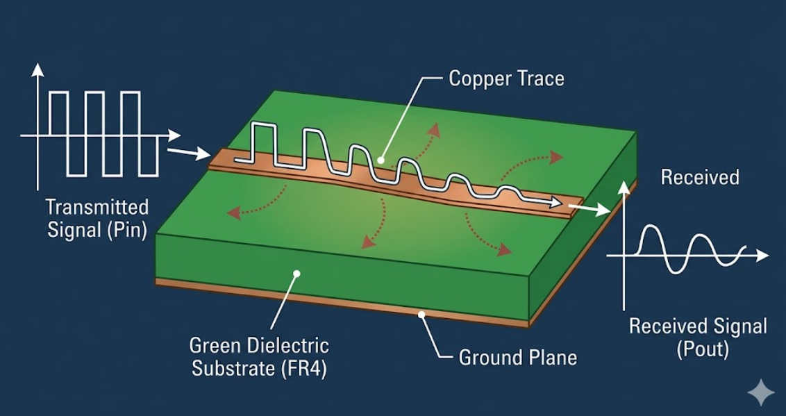
Have you ever designed a high-speed channel on your PCB that – in theory – looked perfect, only to discover that the signal at the receiver was far from what had come out of the transmitter? That aggravating loss of signal strength is referred to as insertion loss. It is one of the most important performance indicators in today's world of high-speed PCB design, and neglecting it could quietly destroy your data links. Insertion loss is an indication of the overall loss of signal power between two points in a transmission line. The value is called S-Parameter and is represented in decibels (dB) (S21 for forward direction or S12 for reverse direction). The simplest form of the insertion loss formula is:
Insertion Loss (dB) = 10 log10 (Pout / Pin)
Where Pout is the power delivered to the load, and Pin is the power into the transmission line. Since there is never an increase in power in a passive channel, insertion loss is always negative. The -3 dB indicates that the signal power is being reduced by 50%.
How Insertion Loss Affects Signal Quality and Data Rate
As the insertion loss rises, the amplitude of the signal at the receiver decreases. But there's more to the issue than poor signals. Insertion loss is frequency-dependent; that is, high-frequency portions of your signal are attenuated more than low-frequency portions. This will change the shape of your digital waveform.
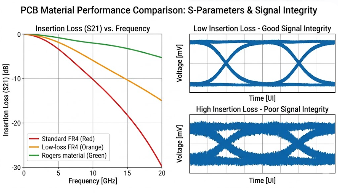
Excessive insertion loss is indicated on an eye diagram as a closed eye opening or a compressed eye opening. The vertical eye height is lowered, which decreases the voltage margin. The width of the eye is reduced horizontally, reducing the timing margin. Both effects raise your bit error rate (BER), and when the eye falls below the receiver threshold, the link fails altogether. The moral of the story is simple. The higher the data rate, the tighter the insertion loss budget. From the laminate you select to the routing of your traces, every design decision directly affects whether or not your channel passes or fails.
Main Factors That Contribute to Insertion Loss
Material Properties: Dielectric Constant and Loss Tangent
Much of the total insertion loss is caused by the dielectric material around your copper traces, particularly frequencies above 1 GHz. There are two material properties that dominate this behavior: the dielectric constant (Dk) and the dissipation factor (Df), or loss tangent. The loss of the dielectric is due to the oscillation of the polar molecules in the substrate caused by the alternating electric field.
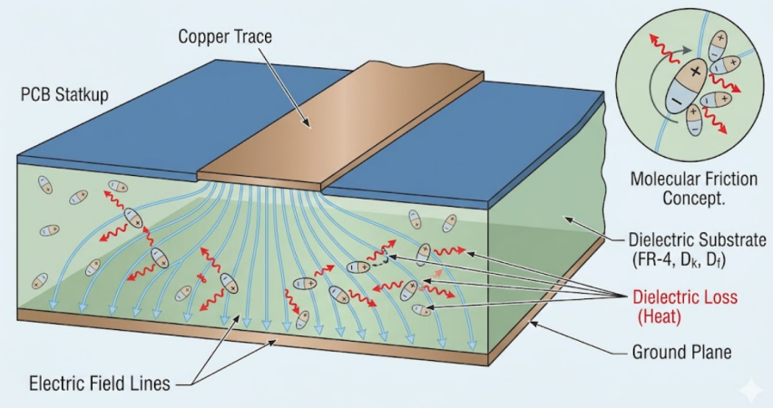
This molecular friction turns the signal energy into heat. The dissipation factor (Df) is a measure of exactly how lossy this process is. The larger the Df, the more energy is lost as heat rather than being transferred to the receiver. The following is a list of Dk and Df for various materials, according to their use cases:
| Material | Dk (at 10 GHz) | Df (at 10 GHz) | Typical Application |
|---|---|---|---|
| Standard FR4 | 4.2 - 4.7 | 0.017 - 0.025 | General digital, up to ~3 GHz |
| Mid-Loss FR4 (e.g., Megtron 4) | 3.8 - 4.0 | 0.005 - 0.010 | 5-10 GHz serial links |
| Low-Loss (e.g., Megtron 6) | 3.4 - 3.7 | 0.002 - 0.004 | 10-25 GHz, PCIe Gen4/5 |
| Rogers RO4003C | 3.38 | 0.0027 | RF, microwave, mmWave |
| Rogers RO4350B | 3.48 | 0.0037 | RF, mixed-signal |
| PTFE/Teflon (RT/duroid 5880) | 2.2 | 0.0009 | mmWave, satellite, 77 GHz radar |
An indirect role is also played by the dielectric constant (Dk). The greater the Dk, the slower the propagation of the signal, and the shorter the wavelengths at any frequency. This makes the electrical length longer, and so the total accumulated dielectric loss over a physical trace run. The lower the Dk, the faster the signal will travel, and the lower the total loss for a given trace length.
Trace Design, Copper Roughness, and Surface Finish Impact
The second big source of insertion loss is conductor loss, which is the loss due to the resistance of the copper traces. Conductor loss is straightforward at DC and low frequency and is based on the trace resistance, which is a function of the trace width, thickness, and copper conductivity. However, at high frequencies, it's a bit more complex. As the frequency increases, the current will tend to flow in a progressively thinner layer near the surface of the conductor. The skin depth of copper is only ~2.1 micrometers at 1 GHz and ~0.66 micrometers at 10 GHz. This is equivalent to increasing the AC resistance of the trace since a smaller cross-sectional area of the copper is conducting.
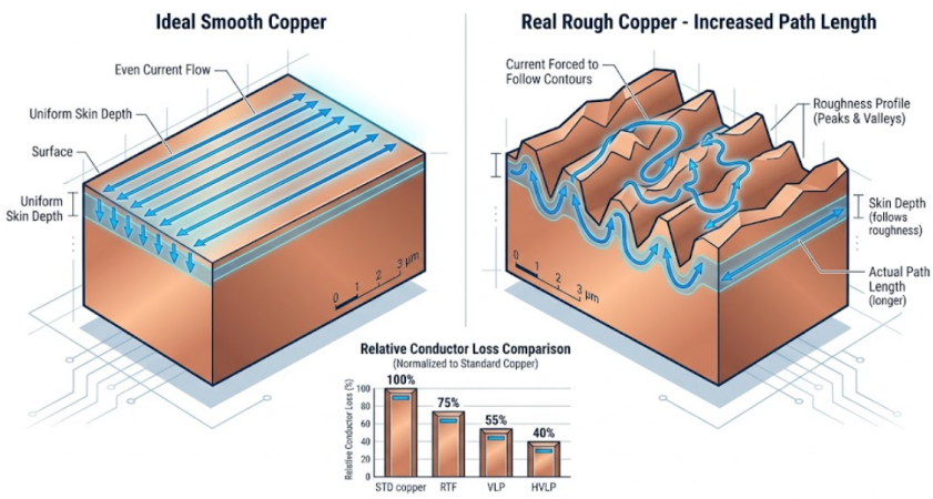
This is where copper roughness is important. Standard electrodeposited (ED) copper has an RMS roughness (Rq) of about 1.0 to 1.8 micrometers. As the skin depth gets closer to the surface roughness, the path that the current follows gets longer and more tortuous. The electrons have to climb over the peaks and dip into the valleys of the rough surface, causing a much higher effective resistance. This is why low-profile copper foils are becoming more and more common in high-speed designs:
- Standard ED Copper (STD): Rq around 1.0 - 1.8 um
- Reverse-treated foil (RTF): Rq around 0.5 - 1.0 um
- Very low profile (VLP): Rq around 0.3 - 0.5 um
- Hyper very low profile (HVLP): Rq around 0.15 - 0.3um
The surface finish also influences the conductor loss at the interface between the conductor and the surface finish. ENIG (Electroless Nickel Immersion Gold) adds a nickel layer that has a much lower conductivity than copper and thus can lead to higher losses on the surface traces. Immersion Silver or OSP (Organic Solderability Preservative) is often used for high-speed surface microstrip lines since it eliminates the lossy nickel barrier layer.
Practical Design Techniques to Minimize Insertion Loss
Optimized Transmission Line Routing and Stackup Planning
The aim is to minimize the dielectric loss and conductor loss by means of smart geometry and layer planning. First, think about the topology of the transmission line. Traces are thinner on inner layers and shave a smaller width for the same impedance goal when using stripline configurations (traces buried between two reference planes), which provide better shielding and often more consistent impedance. Microstrip traces (on outer layers with one reference plane) can be wider with the same impedance, which results in less resistive loss. Embedded microstrip (microstrip covered by prepreg but not between two planes) provides a good compromise for very high-speed channels.
To keep insertion loss under control, follow these trace routing practices:
- Minimize the length of traces as much as practicable. Insertion loss is linear in length. Each millimeter saved directly translates into channel loss savings.
- Minimize via transitions. Loss is added for every via stub and impedance discontinuity. Avoid stubs on high-speed nets by using back-drilled vias or blind/buried vias.
- Use continuous reference planes. Do not cross splits/gaps in reference planes with high-speed signals. The plane discontinuities result in impedance bumps, return path disruptions, and local increases in loss.
- Use appropriate trace widths. The DC and AC resistance of wider traces is lower, which means there is less conductor loss. Use the widest practical trace width, and work with your stackup to get to the desired impedance.
- No unnecessary bends and no serpentine tuning. Each bend causes some small perturbation in the impedance. If you need to match the length of your serpentine, make gentle curves instead of sharp 90-degree cuts.
Stackup directly affects the relationship between trace width, dielectric thickness,s, and impedance. High-speed design requires a well-designed stack-up, with each signal layer accompanied by an adjacent, continuous ground plane. A typical 8-layer high-speed stackup can be described as follows:
| Layer | Function | Notes |
|---|---|---|
| L1 | Signal (microstrip) | High-speed signals, wider traces preferred |
| L2 | Ground plane | Continuous, unbroken reference |
| L3 | Signal (stripline) | Inner high-speed routing |
| L4 | Power plane | PDN, secondary reference |
| L5 | Power plane | PDN, secondary reference |
| L6 | Signal (stripline) | Inner high-speed routing |
| L7 | Ground plane | Continuous, unbroken reference |
| L8 | Signal (microstrip) | High-speed signals, wider traces preferred |
Choosing Low-Loss Materials and Controlled Impedance Strategies
The most important decision for insertion loss performance is material selection. There is no clever routing that can make up for a lossy substrate if your signal frequency requires it. For any high-speed channel, controlled impedance is a requirement. Impedance mismatches result in reflections (return loss), which in turn result in re-reflections that indirectly degrade insertion loss. State tolerances on impedance of +/- 10 % for standard designs, and +/- 5 % for critical channels. Be sure to collaborate with your fabricator to get the stackup you need at the dimensions you can make while achieving your target impedance.
Manufacturing Best Practices for Low Insertion Loss
Precision Etching and Copper Profile Control
Even the highest design goals can be thwarted by manufacturing variation. How the etching is done, which affects the trace geometry, directly influences the insertion loss, since the final trace width, the cross-sectional shape, and the edge profile are defined by the etching process. Chemical etching produces an isotropic etch, which means that the etchant undercuts the copper as well as etching it downwards. This results in a trapezoidal cross-section instead of the commonly assumed ideal rectangular cross-section by most field solvers. Undercut (also known as etch factor) is a function of copper weight, etchant chemistry, and process control. An undercut that is too great will cause a constriction at the top of the trace and result in a smaller cross-sectional area and higher conductor losses. In such high-speed, fine-pitch traces, the following parameters must be carefully controlled by the manufacturer:
- Etch compensation: Widen art to allow for undercut as anticipated
- Etchant concentration and temperature: controlled in a narrow range to ensure uniformity of etch rate
- Conveyor speed (total etch time and uniformity across the panel)
The bonding interface copper foil profile is also controlled by advanced manufacturing equipment. The roughened tooth side of the copper is laminated to the prepreg. As mentioned above, this roughness causes a direct increase in conductor loss at high frequencies. Manufacturers that sell in the high-speed market have low-profile and very-low-profile copper foils that are designed for this purpose.
Advanced Testing and Measurement Methods
A Vector Network Analyzer (VNA) is the typical measurement tool for insertion loss. A VNA sends a standard signal at a variety of frequencies and measures the S-parameters of the DUT. For the S21 parameter, you will directly get the insertion loss. Today, VNAs are available to operate from DC up to 70 GHz or higher to span the entire spectrum of existing high-speed protocols.
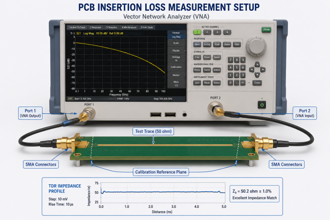
Time Domain Reflectometry (TDR) is another option that can be used in conjunction with VNA measurement to display the impedance profile of the trace. Even if TDR cannot measure the insertion loss directly, it can indicate a change in impedance, which results in reflections and an indirect increase in loss. Built-in TDR is available on many of today's oscilloscopes and VNAs.
JLCPCB's Expertise in Low-Insertion-Loss PCB Production
Premium Low-Loss Materials and High-Precision Fabrication
If low insertion loss is a requirement for your design, then your manufacturer's material stock and process capability will be the deciding factors. In addition to the standard and mid-loss FR4 laminate materials, JLCPCB offers a wide range of high-frequency laminate materials, such as Rogers laminate, Isola laminate, and other high-quality laminate materials.
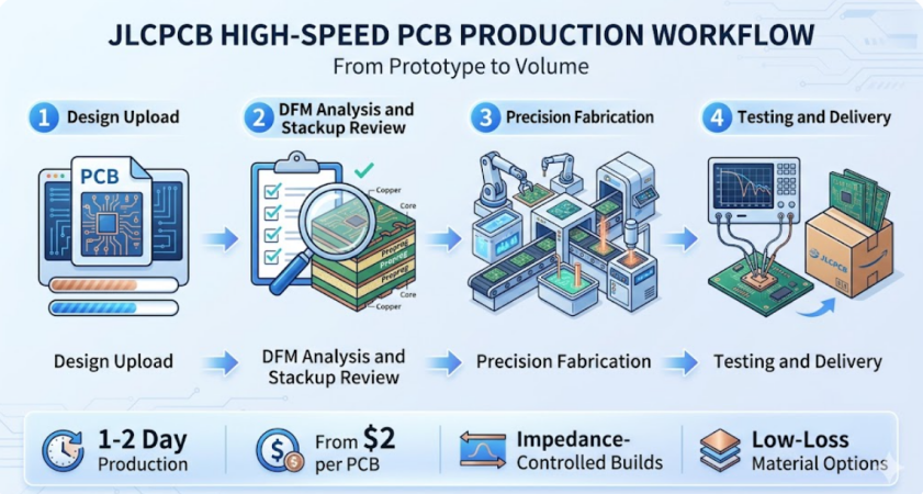
This material flexibility means that you don't have to settle for less. The material can be used for an RF front-end using Rogers RO4350B or in a low-loss FR4 variant for a high-speed digital backplane—either application is available and is ordered from the same platform. JLCPCB's processes are optimized for tight impedance control, and controlled impedance tolerances are available to meet the requirements of multi-gigabit serial links.
Reliable High-Frequency Manufacturing from Prototype to Volume
When it comes to producing high-speed PCBs, consistency is essential. If the prototype is within insertion loss specifications, it is useful only if the production run is of the same quality. All JLCPCB production processes are designed for repeatability,y and in-process controls are put in place to monitor critical parameters throughout the production process.
Production times begin at 1-2 days for standard builds, and pricing begins at $2 for PCBs, so the cost and time to make another iteration with a high-speed design are very low. Requiring a test for three different stackup configurations to determine the optimum insertion loss performance? All three variants are available on your bench in a week.
FAQ about Insertion Loss
Q: What is insertion loss in a PCB?
Insertion loss is the reduction in signal power as it travels through a PCB transmission line. It is measured in decibels (dB) using the S21 S-parameter from a Vector Network Analyzer. A value of -3 dB means half the signal power has been lost.
Q: What are the main causes of insertion loss?
The two primary contributors are dielectric loss (energy absorbed by the substrate material, quantified by dissipation factor Df) and conductor loss (resistive loss in copper traces, worsened by skin effect and copper roughness at high frequencies). Via transitions, connectors, and impedance mismatches also add to the total channel loss.
Q: How do I measure insertion loss on a PCB?
Use a Vector Network Analyzer (VNA) to measure the S21 parameter of a test trace or channel. Design dedicated test coupons on your production panel that match the stackup and trace geometry of your critical nets. Calibrate the VNA properly and de-embed fixture effects for accurate results.
Q: Which PCB materials have the lowest insertion loss?
PTFE-based materials like Rogers RT/duroid 5880 (Df approximately 0.0009) offer the lowest loss. Rogers RO4003C (Df approximately 0.0027) and low-loss FR4 variants like Megtron 6 (Df approximately 0.002-0.004) provide excellent performance at lower cost points. Standard FR4 (Df approximately 0.017-0.025) has the highest loss.
Conclusion
Insertion loss is not simply a specification to check off a compliance list. It is the basic measure that defines if your high-speed channel is providing a clean and reliable data path or noise. As we have discussed throughout this article, it is a part of the design and manufacture that needs attention throughout the entire process, from material selection and copper roughness to trace routing and stackup planning, to etching precision and post-fabrication measurement.
The fortune is that the tools and knowledge to control insertion loss are more readily available than ever. Low-loss laminates are readily available, EDA tools offer in-built field solvers to accurately predict losses, and manufacturers such as JLCPCB can offer material choices and process control for reliable low-loss board fabrication.
Keep Learning
PCB Basics: 50ohm PCB Trace with simple PI matching
When working with the RF (Radio Frequency) design, the transmission of signals between antennas and RF components on a PCB demands careful attention to detail. One critical aspect is the design of the antenna trace, which serves as the conduit for RF signals to propagate efficiently. In this article, we will delve into the significance of maintaining a 50 Ohm characteristic impedance for antenna traces in PCB design, along with best practices for achieving optimal performance in RF applications. Impor......
The Benefits of Coplanar Waveguide in High-Frequency PCB Design
Key Takeaways Coplanar waveguide (especially GCPW) improves high-frequency PCB performance by keeping the return path close and confining fields, which boosts signal integrity and reduces EMI/radiation. It also gives more impedance/layout flexibility (tuning both trace width and gap), but demands tighter manufacturing control of gap tolerances, copper roughness, and material Dk/Df—so field-solver impedance design and DFM checks are essential, with low-loss laminates preferred at higher GHz. Have you e......
6-Layer PCB Stackup and Buildup Guidelines
Printed Circuit Boards (PCBs) are the backbone of modern electronics, providing the necessary infrastructure for connecting and supporting various electronic components. As electronic devices become more complex and compact, the demand for multi-layer PCBs has increased. Among these, the 6-layer PCB is a popular choice for many applications. This article will delve into the specifics of 6-layer PCB stackup, its applications, optimal configurations, and guidelines for selecting the best manufacturer. W......
PCB Antenna Design: Types, Principles, and Best Practices
In the world surrounded with wireless communication, the demand for compact, inexpensive and reliable antennas has never been higher. Antennas are the application of electromagnetic waves. There are many theories and practicals available on antennas, but only few of them get recognised. For wireless data transfer the one solution can be usage of Printed Circuit Board (PCB) antennas. Using PCB antennas represents a convenient solution for integrating them directly into electronic devices, eliminating t......
Designing Antennas on PCB: A Beginner to Advance Guide
In today’s world of widespread wireless connectivity, the demand for small, affordable, and reliable antennas is higher than ever. Antennas act as real-world implementations of electromagnetic wave principles. They enable the sending and receiving of signals for a variety of wireless uses. While there is a lot of theoretical and experimental research in this area, only a few designs become widely used in actual products. Among the different options, Printed Circuit Board (PCB) antennas have become a p......
Backplane Basics: What it is and Why it Matters in High-Speed Electronics
Key Takeaways System Backbone: Backplanes act as passive interconnect boards, routing high-speed data and power across sub-cards without hosting central CPUs. Solderless Press-Fit: They use press-fit connectors to reliably hold thousands of pins while preventing thermal distortion on thick boards. Thick Multilayer Design: Built with 2.0–3.2 mm board thickness, 6–32 layers, and strict ±0.05 mm PTH hole tolerances for superior rigidity. Backdrilling for SI: Controlled-depth backdrilling removes unused v......