Low Loss PCBs : Advanced Materials for Superior High-Speed Signal Performance
14 min
- Understanding Low-Loss PCBs and Their Growing Importance
- Key Benefits of Low-Loss PCB Materials
- Design and Manufacturing Best Practices
- JLCPCB's Advanced Capabilities in Low-Loss PCB Fabrication
- FAQ about Low Loss PCB
- Conclusion
Key Takeaways
Low Loss PCBs using advanced materials like Rogers RO4003C, RO4350B, and PTFE laminates deliver superior signal integrity by dramatically reducing dielectric loss at multi-gigahertz frequencies. Ideal for 5G, mmWave, RF, and high-speed digital designs, these boards offer significantly lower insertion loss, stable impedance, and better thermal performance compared to standard FR4. By choosing the right low-loss laminate and partnering with experienced manufacturers like JLCPCB, engineers can achieve reliable high-frequency performance from prototype to volume production.
As each signal passes through a PCB, it loses a small amount of energy at each stage. In the majority of consumer electronics, it is not a significant loss. But if you are designing circuits to operate at multi-gigahertz frequencies, working with radar systems, or building infrastructure for 5G networks, any extra loss per inch of the order of a few decibels can make or break your design. That's where the low-loss PCB makes the game different. The need for low-loss materials has increased dramatically over the last few years. Standard FR4 just doesn't match the pace of data rates that exceed 25Gbps and RF applications that enter the millimeter-wave band.
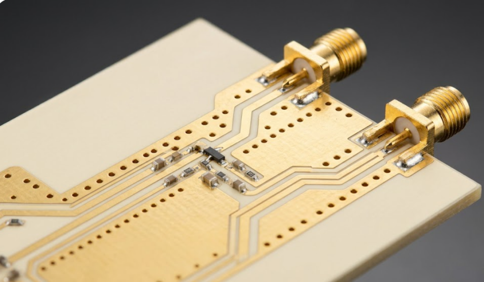
It causes signal amplitude to decay, skews eye diagrams, and creates in-band noise floors that impair receiver sensitivity. For long trace runs and high operating frequency, engineers require materials with good signal fidelity. In this guide, we will go over what is considered “low loss” in a PCB, the top materials in this category, the best practices for designing and manufacturing them, and demonstrate how JLCPCB's advanced PCB fabrication technology for PTFE and Rogers laminates can help you realize these challenging designs.
Understanding Low-Loss PCBs and Their Growing Importance
What Low Loss PCBs Are and How They Work
A low-loss PCB is a printed circuit board that is made using a laminate material with low dielectric loss at high frequencies. Technically, the most important feature is the very low value of the dissipation factor (Df), also referred to as loss tangent (tan delta). The standard FR4 is in the range of 0.017 to 0.025 Df, while true low-loss materials are 0.004 or less, and ultra-low-loss laminates, such as Rogers RT/duroid 5880, are below 0.001.
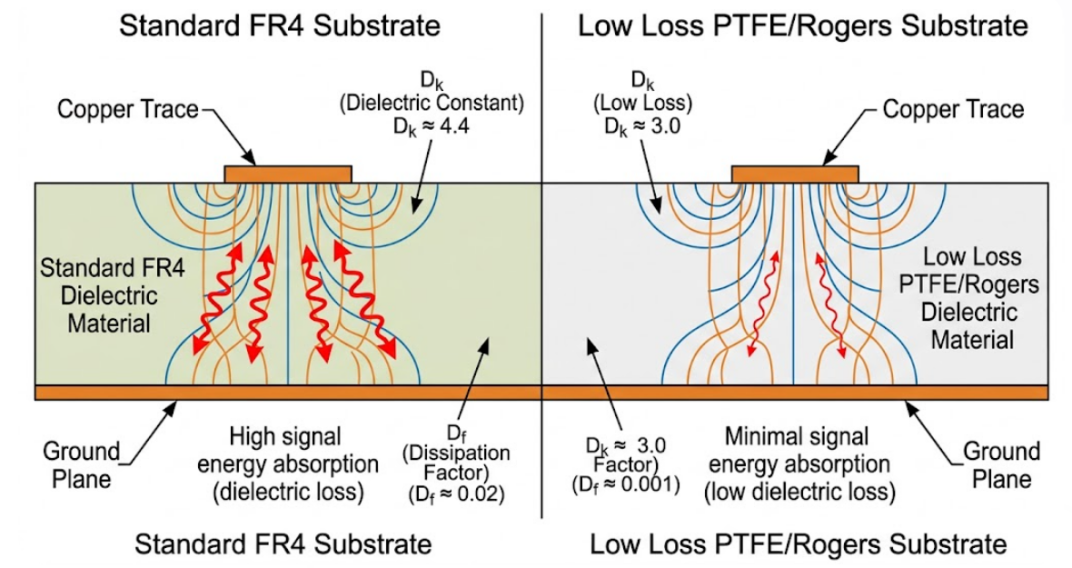
But why is Df so important? As an EM wave travels along a transmission line, it absorbs some of the energy from the transmission line and converts it to heat energy. This is the dielectric loss, and it is higher at higher frequencies and longer traces. The smaller the Df, the less energy will be absorbed, and the more of the original signal will reach the receiver without any change.
There's another reason, too. Low-loss materials also exhibit a low and stable Dk (dielectric constant) over the frequency and temperature range. This stability is of great importance since the Dk is directly related to impedance control in high-speed designs. But if Dk changes as temperature or frequency change, your perfectly engineered 50-ohm trace turns into a different beast, and mismatches and reflections occur.
Why They Are Essential for 5G, RF, and High-Speed Digital Applications
The electronic industry is currently undergoing a giant frequency shift. The FR2 bands are 24.25 GHz to 52.6 GHz for 5G New Radio. The frequency of automotive radar systems is 77 GHz. Ka-band frequencies are from 26.5 to 40 GHz. For these frequencies, the insertion loss per unit length of standard FR4 becomes too large.
Let's look at an example. For a 50 ohm microstrip trace on a standard FR4 (Df ~0.02) at 10 GHz, the insertion loss could be approximately 0.8-1.0 dB per inch. That loss is brought down to about 0.3 dB per inch with the same trace geometry on Rogers RO4003C (Df ~0.0027). That change over 6" of trace translates to over 4 dB of saved signal, and can be the difference between a successful or failed link budget.
Key Benefits of Low-Loss PCB Materials
Significantly Reduced Signal Loss and Better Integrity
The obvious advantage of low-loss materials is simple: a greater amount of your transmitted signal reaches your destination. This can be seen in a number of tangible ways throughout your design.
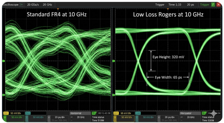
- Reduced insertion loss (S21): Lower insertion loss (S21) indicates that there is less attenuation of the signal per unit length due to the dielectric absorption, which helps to maintain the amplitude of the signal above the threshold of sensitivity of the receiver.
- More open eye diagrams: With less frequency-dependent loss, there is less inter-symbol interference (ISI), leading to wider, more open eye diagrams at the receiver.
- Improved return loss (S11): Stable Dk values allow for tighter impedance control, thereby minimizing reflections and achieving better impedance matching over the bandwidth.
- Minimized phase distortion: When Dk is consistent over frequency, it is possible for different spectral components of a signal to travel at close to the same velocity, maintaining signal shape.
- Reduced noise floor: There is less thermal noise in the substrate due to lower dielectric loss, which gives a better signal-to-noise ratio.
These enhancements directly result in higher receiver sensitivity, longer communication range, and higher data throughput for RF and antenna applications. For digital designs, there are fewer bit errors and a wider margin for the equalization hardware to operate.
Improved Thermal Performance and Long-Term Reliability
Low-loss materials provide advantages beyond just electrical. Many of these expensive laminates are designed for use in extreme environments where the FR4 laminate cannot be used.
For example, materials based on PTFE are very thermally stable and can be modified with ceramic fillers to fit the requirements in terms of coefficient of thermal expansion (CTE). The Rogers RO4000 series laminates feature a thermoset resin system with woven glass reinforcement and have a controlled CTE of about 46 ppm/C in the Z-axis, compared to generic FR4 formulations.
| Property | Standard FR4 | Rogers RO4003C | Rogers RO4350B | PTFE (RT/duroid 5880) |
|---|---|---|---|---|
| Dk (at 10 GHz) | 4.2 - 4.7 | 3.38 | 3.48 | 2.20 |
| Df (at 10 GHz) | 0.017 - 0.025 | 0.0027 | 0.0037 | 0.0009 |
| Moisture Absorption (%) | 0.10 - 0.15 | 0.06 | 0.06 | 0.02 |
| Thermal Conductivity (W/mK) | 0.29 | 0.71 | 0.69 | 0.20 |
| Tg (C) | 130 - 180 | >280 | >280 | N/A (thermoset) |
Balancing Performance, Cost, and Manufacturability
Here is the thing that every engineer faces: the best-performing material is not always the right choice. Selecting a low-loss laminate involves balancing three competing factors, and getting this balance wrong can derail your project.
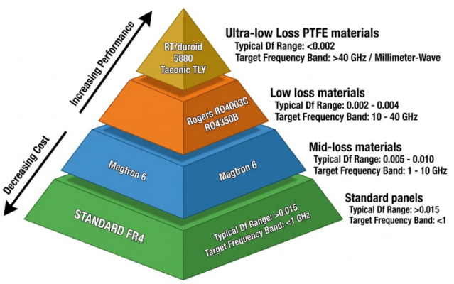
Performance vs. cost: Pure PTFE laminates can cost 5 to 10 times more than standard FR4 per panel. Rogers RO4000 series laminates sit at roughly 2 to 4 times FR4 pricing but offer excellent low-loss performance that satisfies most applications below 20 GHz. Before reaching for the most exotic material, run your link budget analysis and determine the actual Df threshold your design requires.
Manufacturability matters: Not every fabrication house can process every material. PTFE requires specialized drilling parameters (lower feed rates to prevent smearing), modified hole preparation chemistry, and careful handling due to its soft, deformable nature. Rogers RO4000 series, by contrast, processes on the same lines as FR4. This is a major practical advantage.
Hybrid stackups offer a smart compromise. Many designs use a mixed-material approach, placing low-loss laminates only on the layers where RF or high-speed signals are routed, while using standard FR4 or mid-loss materials for power distribution and low-speed digital layers. This keeps costs manageable without sacrificing performance where it counts.
A good rule of thumb for material selection based on frequency is as follows:
| Operating Frequency | Recommended Material Class | Example Laminates |
|---|---|---|
| Below 1 GHz | Standard or mid-loss FR4 | Standard FR4, Isola 370HR |
| 1 - 10 GHz | Low-loss thermoset | Rogers RO4003C, Megtron 6 |
| 10 - 30 GHz | Low loss / ultra-low loss | Rogers RO4350B, Isola Astra MT77 |
| 30 - 77+ GHz | Ultra-low loss PTFE | RT/duroid 5880, Taconic TLY |
Design and Manufacturing Best Practices
Impedance Control and Transmission Line Optimization
Impedance Control and Transmission Line Optimization deals with the control of the transmission line's impedance and optimization of the design. There are some differences in thinking when designing with the low-loss materials compared to the normal FR4 work. The benefits of these materials are the tighter Dk tolerances, but only when they are used properly in the stackup and routing.
Begin with your topology of transmission lines. Microstrip is used on outer layers for most RF designs for ease of component mounting and tuning, and stripline is used on inner layers for better shielding and lower radiation loss. Another great choice is a coplanar waveguide with ground (CPWG), which is especially suitable for mmWave designs requiring tight field confinement.
The following are the key steps to designing a low loss impedance controlled system:
Set your desired Impedance upfront: Typical values are 50 ohm single-ended for RF and 100 ohm differential for high speed digital. The Dk of your material is directly related to the trace width required to achieve these targets.
Adopt the manufacturer suggested Dk values at the operating frequency: Dk at 1 MHz are not valid at 10 GHz. Always use data from the material datasheet that is specific to the frequency.
Include the surface roughness of copper: The roughness of the copper foil is a major factor of loss at frequencies greater than 5 GHz. Use low-profile or very-low-profile (VLP) copper foil (RMS roughness less than 1.5 um) instead of standard electrodeposited copper (3-5 um).
Minimize via transitions: Each signal via creates an impedance mismatch and parasitic inductance. Above 10 GHz, use back-drilled vias or blind/buried via structures to minimize via stub length.
Maintain continuous reference planes: Avoid splits or gaps between the reference ground plane for high-speed and/or RF signals. Impedance discontinuities and increased radiation result from return current disruption.
Use stitching along transmission lines to apply: To suppress parallel plate modes and waveguide effects, introduce ground vias at regular intervals (less than lambda/20 at the highest frequency of interest) for CPWG and shielded stripline designs.
Precision Etching and Process Consistency
However, fabricating low-loss PCBs requires more process control than regular FR4 manufacturing. The material reacts differently in the process of drilling, etching, and laminating,n and a fabricator not used to working with these types of materials will yield inconsistent results.
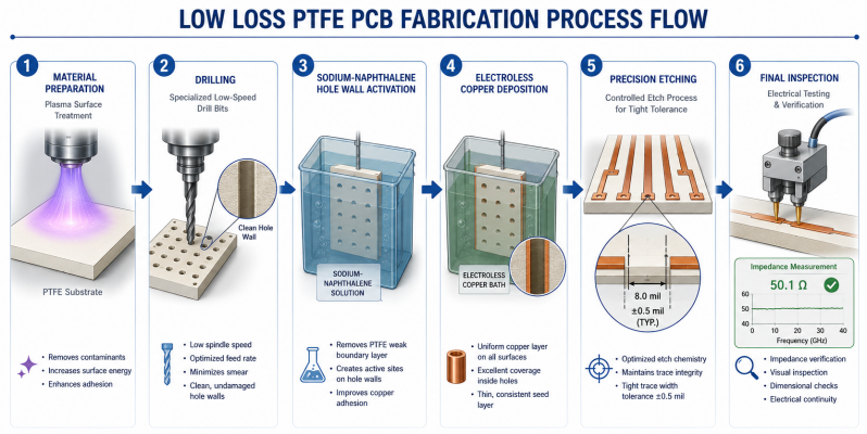
- Drilling: PTFE materials are soft and have a tendency to smear during mechanical drilling. The spindle speed has to be reduced, the feed rate decreased, and special bits with modified geometries must be used. Laser drilling using CO2 or UV laser is preferred for microvias because they can be drilled without mechanical deformation, resulting in cleaner holes.
- Copper adhesion: PTFE is intrinsically not adherent to copper. To achieve bonding to the electroless copper deposition step, the surface of the parts must be treated with plasma or sodium-naphthalene. If not treated, copper will delaminate from the substrate during thermal cycling.
- Etching precision: In mmWave frequencies, even a 0.5 mil (12.7 um) variation in the trace width will cause a change of impedance by several ohms. To control the impedance of the PCB across the panel, the etching tolerance needs to be tight, usually within 0.5 mil or less for low-loss PCB fabrication.
Hybrid stackups (PTFE or Rogers with FR4 layers) will need to be laminated with controlled lamination profiles. There are various materials with different flow characteristics and cure temperatures, and the press cycle should be able to accommodate all materials in the stackup without over-curing or under-bonding any of the layers.
JLCPCB's Advanced Capabilities in Low-Loss PCB Fabrication
Premium Material Partnerships and High-Precision Production
In the field of low-loss PCB fabrication, JLCPCB has spent a lot of money on materials and process capabilities. JLCPCB provides engineers with the two most trusted material families in the RF and high-speed domain: PTFE and Rogers laminates. This allows for the use of materials such as Rogers RO4003C, RO4350B, and PTFE-based laminates, and the use of a manufacturer that has the specific knowledge of processing for each material.
Whether the substrates are PTFE or require precision etching for tight impedance tolerances, JLCPCB's production lines are designed to meet these challenging requirements. This brings a fabrication partner that is ready to provide the necessary precision and consistency required by low-loss designs without the long lead times and high costs that have been common with more advanced material PCBs.
Reliable Scalable Manufacturing from Prototype to Volume
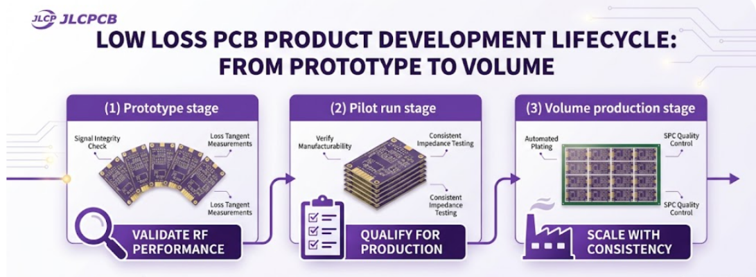
For low-loss PCB projects, a ramp-up starting with a few prototypes for validation, followed by a small pilot run, and then scaling to volume production is often experienced. At every stage, JLCPCB ensures quality, supporting this entire lifecycle. Ordering just 5 boards for prototype testing can be done with fast turnaround, which will allow you to test your RF for your application on real hardware before going through the process of a larger run.
Once you are ready to scale, the same process controls and material sourcing are all applicable to production, ensuring that the boards you qualified in prototyping are the same as those you will receive in production. This prototype-to-production consistency is very important for low-loss designs, as RF performance is very sensitive to manufacturing variation. The etching chemistry or lamination pressure from your prototype to your production batch can vary by tenths of a decibel, which can make a significant difference in a tightly budgeted mmWave link.
FAQ about Low Loss PCB
Q: What is a low-loss PCB?
A low-loss PCB is a printed circuit board made with laminate materials that have a very low dissipation factor (Df), typically below 0.005. These materials minimize the amount of signal energy absorbed by the substrate at high frequencies, resulting in lower insertion loss and better signal integrity.
Q: When should I use a low-loss CB material instead of standard FR4?
Consider low-loss materials when your design operates above 1 GHz and signal integrity is critical, when your link budget analysis shows that FR4 dielectric loss causes unacceptable signal attenuation, or when you are working with RF, mmWave, 5G, or high-speed digital protocols like PCIe Gen4/Gen5.
Q: What is the difference between Rogers and PTFE laminates?
Rogers RO4000 series laminates use a ceramic-filled hydrocarbon thermoset resin system and can be processed on standard FR4 fabrication equipment. PTFE (Teflon-based) laminates like RT/duroid 5880 offer even lower losses but require specialized manufacturing processes.
Q: Does JLCPCB support low-loss PCB fabrication?
Yes. JLCPCB mainly supports PTFE and Rogers laminates for low-loss PCB fabrication. Their production capabilities include the specialized processing these materials require, along with DFM engineering review, impedance-controlled manufacturing, and consistent quality.
Conclusion
The use of low-loss PCBs is no longer a military niche requirement, since they are used in satellite systems and military radar. As the world moves toward the mainstream of 5G, automotive radar, high-speed networking, and IoT edge computing, materials that maintain signal integrity at multi-gigahertz frequencies are increasingly in demand. The three keys to a successful low-loss design are understanding the role of dissipation factor, choosing the appropriate laminate for your frequency range, and working with a manufacturer with proven process capability for these materials.
The lesson here is that in the low-loss world, material selection and manufacturing execution go hand-in-hand. Even the best laminate in the world will be suboptimal if it is made by a shop that doesn't know how to process the laminate. With support for PTFE and Rogers laminates, along with DFM review and consistent prototype-to-production quality, JLCPCB is a great option for engineers who require low-loss performance without the traditional cost and lead time. For a high-frequency or high-speed design, try JLCPCB's high-quality material options and discover how they can help you create your next project.
Keep Learning
PCB Basics: 50ohm PCB Trace with simple PI matching
When working with the RF (Radio Frequency) design, the transmission of signals between antennas and RF components on a PCB demands careful attention to detail. One critical aspect is the design of the antenna trace, which serves as the conduit for RF signals to propagate efficiently. In this article, we will delve into the significance of maintaining a 50 Ohm characteristic impedance for antenna traces in PCB design, along with best practices for achieving optimal performance in RF applications. Impor......
The Benefits of Coplanar Waveguide in High-Frequency PCB Design
Key Takeaways Coplanar waveguide (especially GCPW) improves high-frequency PCB performance by keeping the return path close and confining fields, which boosts signal integrity and reduces EMI/radiation. It also gives more impedance/layout flexibility (tuning both trace width and gap), but demands tighter manufacturing control of gap tolerances, copper roughness, and material Dk/Df—so field-solver impedance design and DFM checks are essential, with low-loss laminates preferred at higher GHz. Have you e......
6-Layer PCB Stackup and Buildup Guidelines
Printed Circuit Boards (PCBs) are the backbone of modern electronics, providing the necessary infrastructure for connecting and supporting various electronic components. As electronic devices become more complex and compact, the demand for multi-layer PCBs has increased. Among these, the 6-layer PCB is a popular choice for many applications. This article will delve into the specifics of 6-layer PCB stackup, its applications, optimal configurations, and guidelines for selecting the best manufacturer. W......
PCB Antenna Design: Types, Principles, and Best Practices
In the world surrounded with wireless communication, the demand for compact, inexpensive and reliable antennas has never been higher. Antennas are the application of electromagnetic waves. There are many theories and practicals available on antennas, but only few of them get recognised. For wireless data transfer the one solution can be usage of Printed Circuit Board (PCB) antennas. Using PCB antennas represents a convenient solution for integrating them directly into electronic devices, eliminating t......
Designing Antennas on PCB: A Beginner to Advance Guide
In today’s world of widespread wireless connectivity, the demand for small, affordable, and reliable antennas is higher than ever. Antennas act as real-world implementations of electromagnetic wave principles. They enable the sending and receiving of signals for a variety of wireless uses. While there is a lot of theoretical and experimental research in this area, only a few designs become widely used in actual products. Among the different options, Printed Circuit Board (PCB) antennas have become a p......
Backplane Basics: What it is and Why it Matters in High-Speed Electronics
Key Takeaways System Backbone: Backplanes act as passive interconnect boards, routing high-speed data and power across sub-cards without hosting central CPUs. Solderless Press-Fit: They use press-fit connectors to reliably hold thousands of pins while preventing thermal distortion on thick boards. Thick Multilayer Design: Built with 2.0–3.2 mm board thickness, 6–32 layers, and strict ±0.05 mm PTH hole tolerances for superior rigidity. Backdrilling for SI: Controlled-depth backdrilling removes unused v......