
Achieving Reliable High-Speed Performance with PCB Transmission Lines
11 min
- What PCB Transmission Lines Are and Why They Matter
- Key Types of PCB Transmission Lines
- Essential Design Techniques for Optimal Transmission Lines
- Manufacturing Considerations for High-Performance Transmission Lines
- JLCPCB's Expertise in High-Speed Transmission Line PCBs
- FAQ about PCB Transmission Line
Key Takeaways
PCB Transmission Lines are essential for reliable high-speed PCB performance in USB 3.0, PCIe, DDR4, and RF designs, turning traces into controlled-impedance structures that eliminate reflections, crosstalk, and attenuation. Select microstrip, stripline, or GCPW geometries with accurate calculations, continuous reference planes, mitered bends, and 3W spacing, then rely on precise etching, copper profile control, and TDR testing at JLCPCB for consistent results from prototype to volume production.
Have you ever traced a board that checked all the design rule checks, but the prototype displayed ringing on clock lines or eye diagrams that were more likely to be smudges than clean holes? Your copper traces are not just connections in high-speed design. They are PCB transmission lines, and the simplest method to kill signal integrity is to treat these lines like simple wires. When the rise time of your signal is sufficiently small that the trace length is a substantial portion of the wavelength, all details of that trace count. Whether your signal is clean or corrupted is determined by the width, the distance to the reference plane, the dielectric material, and even how it rounds a corner.
In interfaces such as USB 3.0, PCIe, and DDR4, this limit is reached with trace lengths just a few centimeters long. This article will discuss the concept of PCB transmission lines, the most important types in actual designs, the most important techniques used to obtain controlled impedance, and the manufacturing issues that transform a good design into a high-quality product.
What PCB Transmission Lines Are and Why They Matter
Understanding Transmission Lines in High-Speed and RF Designs
A transmission line PCB design is any copper trace whose electrical properties are determined by its distributed inductance and capacitance, and not by mere DC resistance. When the length of a trace is more than about a tenth of the signal wavelength, it turns into a transmission line, with voltage and current traveling as electromagnetic waves in the trace geometry and the dielectric around it.
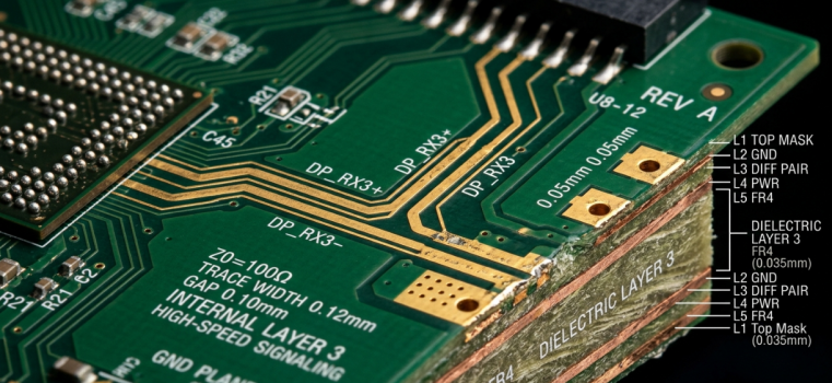
Characteristic impedance is dependent on trace width, copper thickness, dielectric constant (Dk) of substrate, and distance to reference ground plane. With a trace width of 8 to 12 mils, a microstrip can be used to obtain a 50 ohm transmission line impedance of a standard FR4 (Dk 4.2 to 4.7). The 50 ohm standard is the basis of most RF components, connectors, and interface standards.
Common Signal Integrity Challenges They Solve
When transmission lines are not properly designed, a predictable set of problems emerges:
- Reflections occur whenever impedance changes along the signal path. A trace that widens, passes over a ground plane gap, or meets a mismatched load creates ringing and overshoot that cause false triggering.
- Crosstalk is the undesired interaction between neighboring traces. Close parallel traces cause near-end crosstalk (NEXT) and far-end crosstalk (FEXT) on adjacent signals.
- Attenuation: The progressive loss of signal due to the conductor resistance and dielectric absorption. At higher frequencies (above 1 GHz), dielectric loss can be the major factor, so material choice becomes essential.
Key Types of PCB Transmission Lines
Microstrip, Stripline, and Coplanar Waveguide Options
There are three fundamental transmission line geometries in PCB design. Microstrip is the most common, consisting of a trace on an outer layer with a ground plane on the adjacent inner layer. The signal propagates through a mix of substrate and air, giving an effective Dk of 3.3 to 3.8 on FR4 and a propagation delay of approximately 6 ps/mm.
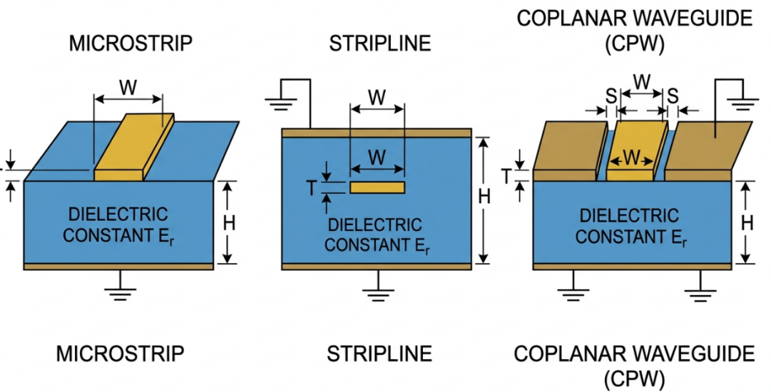
Stripline is a trace embedded between two ground planes on the inner layers. Fully enclosed by dielectric, it offers superior EMI shielding and more consistent impedance, with a propagation delay of approximately 7 ps/mm on FR4. It requires at least a 4-layer board.
A coplanar waveguide (CPW) places ground conductors on the same layer as the signal trace, flanking it on both sides. The grounded variant (GCPW) adds a ground plane beneath. CPW is popular in RF and mmWave designs for its excellent impedance control and easy component integration without ground vias.
| Parameter | Microstrip | Stripline | Coplanar Waveguide (GCPW) |
|---|---|---|---|
| Trace Location | Outer layer | Inner layer (between planes) | Outer layer with coplanar grounds |
| Effective Dk (FR4) | 3.3 to 3.8 | 4.2 to 4.7 | 3.5 to 4.0 |
| Propagation Delay (FR4) | ~6 ps/mm | ~7 ps/mm | ~6.2 ps/mm |
| EMI Shielding | Moderate | Excellent | Good |
| Minimum Layers | 2 | 4 | 2 |
| Common Applications | USB, HDMI, general digital | DDR, high-speed buses | RF, mmWave, 5G |
Choosing the Right Type for Your Application
The choice of the type relies on frequency range, EMI considerations, and the budget for the number of layers:
- General high-speed digital (USB, PCIe, HDMI): The default is microstrip. Very easy to design, very easy to inspect, and can be used with most PCB transmission line calculator tools.
- High-speed buses (DDR4/5, multi-lane PCIe): Stripline offers superior crosstalk isolation between closely-spaced differential pairs.
- RF and microwave (above 6 GHz): GCPW has the lowest radiation loss and impedance control in the millimeter-wave frequencies.
- Mixed-signal boards: Use stripline with sensitive analog signals and microstrip with less sensitive digital interfaces.
A combination on the same board is frequently used in many designs. A 6-layer PCB could have DDR4 stripline on the inner layers and USB microstrip on the outer layers.
Essential Design Techniques for Optimal Transmission Lines
Impedance Calculation and 50 Ohm Line Design
For a microstrip, the characteristic impedance can be approximated as:
Z0 = (87 / sqrt(Er + 1.41)) x ln(5.98 x H / (0.8 x W + T))
Where Er is the dielectric constant, H is the dielectric height to the ground plane, W is the trace width, and T is the copper thickness. The width of a 50 ohm FR4 (Er = 4.4) microstrip with 1 oz copper and 8 mil dielectric height would be about 14.5 mil. The width required is approximately 18 mil on Rogers RO4003C (Er = 3.38).
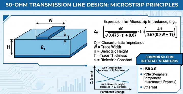
Finally, there should be a PCB transmission line calculator. EasyEDA, Altium, and Saturn PCB Toolkit tools consider etch profile and frequency-dependent properties that are not included in easy formulas. In the case of differential pairs, USB 3.0 targets 90 ohm, PCIe targets 100 ohm, DDR targets 100ohms,m and LVDS targets 100 ohm.
Routing Rules, Bend Optimization, and Ground Plane Strategies
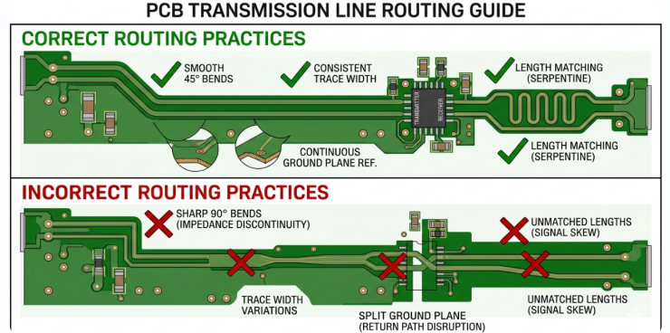
Once trace widths are defined, routing execution determines whether the impedance stays controlled.
Maintain a continuous reference plane. The return current follows the path of least impedance directly beneath the signal trace. Never route high-speed signals over plane splits, slots, or voids. This is the single most important rule.
Optimize bends to avoid impedance discontinuities:
1.Use 45-degree mitered bends for standard high-speed digital designs
2.Use curved bends with a radius of at least 3x trace width for RF above 10 GHz
3.Avoid 90-degree corners, which create capacitive discontinuities at high frequencies
Minimize via transitions. Each via introduces parasitic inductance. Place ground stitching vias adjacent to every signal via to provide a low-inductance return path. For differential pairs, place ground vias on both sides of the signal via pair.
Use the 3W space rule: Ensure that there is at least three times the trace width between adjacent traces to ensure that crosstalk is below about -40 dB. On differential pairs, match with length equal to that of the pairs, but serpentine tuning (not tight accordion) should be used.
Manufacturing Considerations for High-Performance Transmission Lines
Precise Etching, Copper Profile Control, and Layer Registration
Your design geometry should be replicated faithfully in the manufacturing process, since even minor variations have a direct impact on the impedance realized. The accuracy of the trace width is determined by etching. Chemical etching is used to etch copper both laterally and vertically (undercut), forming a trapezoidal cross-section. Normal undercut decreases width by 0.5-1.5 mil each side. Manufacturers make it up by pre-widening artwork, which is calibrated to each copper weight.
Above 3 GHz, copper surface roughness is important. The skin effect causes current to be limited to the conductor surface, and coarse surfaces enhance loss. Roughness of standard foil is 1 to 2 micrometers, and low-profile foils of 0.3 to 0.5 micrometers are 0.5 to 1.0 dB/inch less than 10 GHz. The accuracy of registering the layer is plus or minus 2 to 3 mils, which causes traces to move relative to the ground plane, changing dielectric height and impedance.
Ensuring Consistent Impedance Across Production
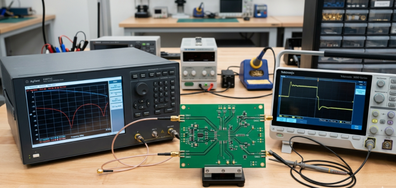
Manufacturers use impedance test coupons on every production panel, measured with a time domain reflectometer (TDR), to verify impedance at every point along the test trace. Achieving tight tolerances requires:
1.Dielectric thickness control to within plus or minus 0.5 mil during lamination
2.Etch compensation maintaining trace width within plus or minus 0.5 mil
3.Consistent copper plating thickness across the panel
4.Stable lamination profiles for a uniform dielectric constant
5.Regular TDR calibration and coupon validation
| Impedance Tolerance | Trace Width Control | Dielectric Control | Typical Application |
|---|---|---|---|
| +/- 10% | +/- 1.0 mil | +/- 1.0 mil | General high-speed digital |
| +/- 7% | +/- 0.75 mil | +/- 0.75 mil | USB 3.0, PCIe Gen3/4 |
| +/- 5% | +/- 0.5 mil | +/- 0.5 mil | RF, mmWave, PCIe Gen5 |
JLCPCB's Expertise in High-Speed Transmission Line PCBs
Advanced Fabrication for Accurate Impedance and Low Loss
When your design demands controlled impedance, the manufacturer matters. JLCPCB's process begins with precise stackup management using well-characterized materials like Shengyi S1000-2M and NP-155F. For higher frequencies, Rogers, PTFE, and hybrid stackups are supported, with each material's Dk profiled in the impedance tools. Every impedance-controlled order is verified using TDR coupon testing on the same production panel, targeting plus or minus 10 percent tolerance with tighter options available.
Integrated DFM Support and High-Frequency Manufacturing Capabilities
JLCPCB's DFM review catches transmission line-specific issues before fabrication, evaluating:
- Trace widths are too narrow for reliable etching at the selected copper weight
- Dielectric heights that cannot achieve the requested impedance
- Via placements that create impedance discontinuities
- Ground plane voids that disrupt return current paths
For engineers using EasyEDA, the stackup editor and impedance calculator are tied directly to JLCPCB's materials and process capabilities. The impedance values you calculate during design match what you get in production. Advanced features include controlled impedance on inner and outer layers, via-in-pad with epoxy fill, and edge-plated ground connections for GCPW structures.
Reliable Production from Prototypes to Volume Runs
JLCPCB maintains the same process parameters from prototype through volume production. The stackup, etch compensation, and lamination profiles from your prototype are reused for production runs, ensuring consistent signal integrity. With production starting from $2 and turnaround as fast as 1 to 2 days, you can iterate quickly on impedance-sensitive designs, validate with TDR measurements, and scale to volume with confidence.
FAQ about PCB Transmission Line
Q: What is a transmission line in PCB design?
A transmission line is a copper trace whose behavior is dominated by distributed inductance and capacitance rather than DC resistance. This happens when trace length exceeds roughly one-tenth of the signal wavelength, making the trace geometry the primary factor controlling signal propagation.
Q: Why is 50 ohms the standard for PCB transmission lines?
It is a compromise between minimum attenuation (around 77 ohms) and maximum power handling (around 30 ohms). Decades of standardization around 50 ohm connectors and test equipment have cemented it as the universal default.
Q: What is the difference between microstrip and stripline?
Microstrip runs on an outer layer with one ground plane beneath it. Stripline runs on an inner layer between two ground planes, offering better EMI shielding but requiring at least a 4-layer board. Microstrip is simpler and allows direct component access.
Q:Does the ground plane affect transmission line impedance?
Absolutely. The ground plane is half of the transmission line structure. Any discontinuity, such as splits or voids, disrupts the return current path and creates impedance discontinuities. A solid, continuous ground plane is the most important rule for impedance control.
Keep Learning
Building Reliable High-Speed Performance with Effective Timing Analysis
Key Takeaways Timing analysis is essential for high-speed PCBs — clean signals can still fail if they miss setup or hold windows. Focus on setup time, hold time, clock skew, and propagation delay to ensure reliable data sampling. Prioritize length matching, controlled impedance, and proper stackup to maintain positive timing margins. Combine static timing analysis with dynamic simulation for best results. Precision manufacturing is critical — small variations in impedance or dielectric thickness can d......
Low Loss PCBs : Advanced Materials for Superior High-Speed Signal Performance
Key Takeaways Low Loss PCBs using advanced materials like Rogers RO4003C, RO4350B, and PTFE laminates deliver superior signal integrity by dramatically reducing dielectric loss at multi-gigahertz frequencies. Ideal for 5G, mmWave, RF, and high-speed digital designs, these boards offer significantly lower insertion loss, stable impedance, and better thermal performance compared to standard FR4. By choosing the right low-loss laminate and partnering with experienced manufacturers like JLCPCB, engineers ......
How to Reduce Insertion Loss for Better High-Speed PCB Performance
Key Takeaways Reducing insertion loss is essential for achieving reliable high-speed PCB performance. By selecting low-loss materials with lower Df, optimizing trace routing and stackup design, minimizing via transitions, using smoother copper foils, and applying precision manufacturing techniques, designers can significantly lower both dielectric and conductor losses. These strategies help maintain better signal integrity, wider eye openings, and higher data rates in multi-gigabit designs. Have you e......
How to Create the Perfect PCB Stackup for High-Speed and Reliable Designs
Key Takeaways A well-designed PCB stackup is the foundation of high-speed, reliable designs, determining signal integrity, controlled impedance, and EMI performance. Use symmetrical layers with adjacent reference planes, proper dielectric spacing, and copper balancing to avoid warpage and crosstalk. Choose standard FR4 for <3 GHz or low-loss materials (Megtron 6, Rogers) for higher speeds, and work closely with manufacturers for optimal results. Mastering your stackup is essential for high-speed succe......
Achieving Reliable High-Speed Performance with PCB Transmission Lines
Key Takeaways PCB Transmission Lines are essential for reliable high-speed PCB performance in USB 3.0, PCIe, DDR4, and RF designs, turning traces into controlled-impedance structures that eliminate reflections, crosstalk, and attenuation. Select microstrip, stripline, or GCPW geometries with accurate calculations, continuous reference planes, mitered bends, and 3W spacing, then rely on precise etching, copper profile control, and TDR testing at JLCPCB for consistent results from prototype to volume pr......
Backdrill Vias: Enhancing Signal Integrity in High-Speed PCBs
Key Takeaways Backdrill vias remove unused copper stubs from plated through-hole vias, shortening the residual stub to under 0.15 mm (6 mils). This eliminates impedance discontinuities, reflections, and resonances in high-speed signals above 5–10 Gbps. It delivers better return loss, insertion loss, lower jitter, and clearer eye diagrams — all while keeping simple stack-ups and far lower cost than blind/buried vias. Use backdrilling for any stub longer than 15 mils (0.381 mm), especially on boards thi......