
How to Create the Perfect PCB Stackup for High-Speed and Reliable Designs
13 min
- Why a Well-Designed PCB Stackup Is Critical
- Key Principles of Effective PCB Stackup Design
- Choosing the Right Materials and Configurations
- Manufacturing Considerations for Reliable Stackup Implementation
- JLCPCB's Expertise in Advanced PCB Stackup Fabrication
- FAQ about PCB Stackup
- Conclusion
Key Takeaways
A well-designed PCB stackup is the foundation of high-speed, reliable designs, determining signal integrity, controlled impedance, and EMI performance. Use symmetrical layers with adjacent reference planes, proper dielectric spacing, and copper balancing to avoid warpage and crosstalk. Choose standard FR4 for <3 GHz or low-loss materials (Megtron 6, Rogers) for higher speeds, and work closely with manufacturers for optimal results. Mastering your stackup is essential for high-speed success.
Have you ever laid out a gorgeous 6-layer PCB, and then passed all your DRCs and still gone to sleep at night, with signal integrity after fabrication? Most likely, it was not your routing. Your PCB stackup was. A layer stackup is the structural basis of any multilayer board, and a poor choice can quietly ruin even the most painstakingly routed designs. A designed PCB stackup defines the path of signals, the distribution of power, and the level of rejection of electromagnetic interference by your board. The stackup is where performance starts, whether you are creating a USB 3.0 hub or a DDR4 memory interface. Today, we will take a tour of all the information you will need to know about PCB stackup design, starting with how to arrange the layers and how to make them symmetrical, up to what material to use, how to design impedance, and how to manufacture.
Why a Well-Designed PCB Stackup Is Critical
The Role of Stackup in Signal Integrity and Power Integrity
Any high-speed signal on your PCB is a transmission line. The impedance of that transmission line depends on the trace width, distance to the reference plane, and the dielectric constant of the material between the traces. All three parameters are defined by your stackup. To assure signal integrity, an optimally fabricated stackup provides controlled impedance on important nets. USB 3.0 has a 90-ohm differential impedance requirement, PCIe has 85 ohms, and the data lines of DDR4 must be carefully matched with controlled impedance. These targets can hardly be achieved without the right stackup.
To achieve power integrity, stackup defines the performance of your power delivery network. When the power and ground planes are in close proximity, naturally distributed capacitance, commonly referred to as interplane capacitance, is produced. A 4-mil dielectric spacing between a pair of tightly-paired power and ground planes can yield about 90 pF/square inch. This inherent capacitance can be used to reduce high-frequency noise without extra decoupling devices.
Common Problems Caused by Poor Stackup Choices
Poorly conceived stackup results in issues that are hard and costly to resolve post-fabrication:
- Impedance mismatch: Dielectric thickness is inaccurately set and results in an impedance mismatch, which results in signal reflections and poor eye diagrams.
- Excessive crosstalk: NEXT and FEXT crosstalk can be coupled with a trace-to-trace in the case of two signal layers separated by no ground plane.
- EMI radiation: Signals that do not have a continuous reference plane emit electromagnetic energy at board edges and slots in return paths.
- Warpage and delamination: An asymmetric stackup leads to uneven lamination stress, which results in warpage and unreliable solder joints.
- Power supply noise: Power and ground planes are far apart to provide the lowest interplane capacitance.
These issues are added to the growing signal speed. A 100 MHz design may be able to survive a mediocre stackup, whereas a 5 Gbps SerDes link will not.
Key Principles of Effective PCB Stackup Design
Layer Arrangement, Symmetry, and Balance Rules
Symmetry is the first stackup design rule. The arrangement of the layers over the center of the board should be a reflection of the arrangement under the board. This is not merely a design choice, but a manufacturing necessity. Asymmetric stackups result in differential stress in the lamination cooling process, which results in board warpage.
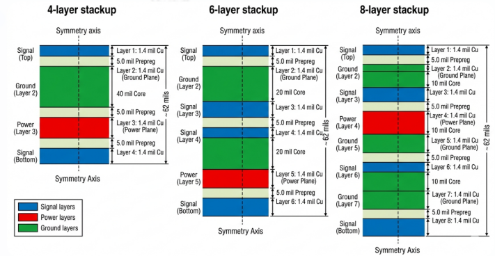
For a standard 4-layer board, the classic arrangement is:
| Layer | Function | Typical Thickness |
|---|---|---|
| L1 (Top) | Signal + Components | 1.2 mil (copper) + prepreg to L2 |
| L2 | Ground Plane (GND) | 1.2 mil (copper) |
| L3 | Power Plane (VCC) | 1.2 mil (copper) |
| L4 (Bottom) | Signal + Components | 1.2 mil (copper) + prepreg from L3 |
This design offers every signal layer an adjacent reference plane to control impedance, and the GND and VCC planes create a loosely coupled pair to deliver power. In 6-layer and 8-layer designs, the same concepts are applicable. Where feasible, always alternate signal layers with plane layers.
Impedance Control and Reference Plane Strategies
The control of impedance begins in the stackup, not the router. The characteristic impedance of a trace on a microstrip or stripline stackup is a function of three parameters that are defined by the stackup: dielectric thickness, dielectric constant (Dk), and copper weight. In a microstrip on FR4 (Dk of about 4.2 to 4.5), a 50-ohm single-ended impedance would be achieved with a trace width of 4 to 5 mils with a 4-mil dielectric to reference plane. The following are the most important strategies of reference plane management:
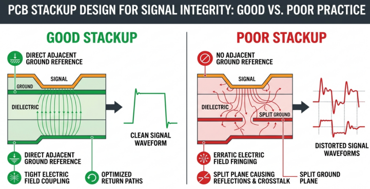
1.Each signal layer should have a continuous reference plane on an adjacent layer.
2.Ground planes but not power planes should be used as the reference for high-speed differential pairs.
3.When a signal passes through layers using a via, make both reference planes an identical net. Otherwise, install stitching vias in the area of the return current.
4.Do not divide a ground plane along a high-speed signal route. The diverted return current forms a huge loop, which radiates EMI.
5.Suppress plane-to-plane cavity resonance between board edges with ground stitching vias.
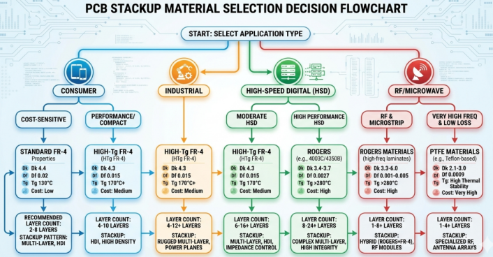
Choosing the Right Materials and Configurations
Low-Loss Laminates and Prepreg Options
The workhorse of the PCB industry is FR4, which has a Dk of about 4.2-4.7 and a Df of about 0.017-0.025. In designs with frequencies under 3 GHz, standard FR4 is quite suitable and economical. Above 5 GHz frequencies, dielectric loss is a critical issue. Here comes the low-loss laminates into the scene:
| Material | Dk (at 10 GHz) | Df (at 10 GHz) | Tg (C) | Typical Use Case |
|---|---|---|---|---|
| Standard FR4 | 4.2 - 4.7 | 0.017 - 0.025 | 130 - 140 | General-purpose, < 3 GHz |
| Mid-Tg FR4 | 4.2 - 4.5 | 0.015 - 0.020 | 150 - 160 | Automotive, industrial |
| High-Tg FR4 | 4.0 - 4.4 | 0.012 - 0.018 | 170 - 180 | Lead-free assembly, server |
| Megtron 6 (Panasonic) | 3.4 | 0.002 | 185 | 10+ Gbps SerDes, backplanes |
| Rogers RO4003C | 3.38 | 0.0027 | 280 | RF, microwave to 40 GHz |
| Rogers RO4350B | 3.48 | 0.0037 | 280 | RF power amplifiers |
| PTFE (Teflon) | 2.1 - 2.2 | 0.0009 | 327 | mmWave, 77 GHz radar |
Prepreg (pre-impregnated fiberglass) is the bonding agent between the copper and core layers when laminating. There are 106, 1080, 2116, and 7628 standard glass styles with varying resin content and thickness. Tight dielectric spacing is done with thinner prepregs (106, 1080), whereas thicker prepregs (2116, 7628) are more mechanically strong.
Standard vs. Custom Stackup for Different Applications
Not all designs require a custom stackup. In most of the applications, a standard stackup of a manufacturer is economical in terms of cost and lead time.
Standard stackups are suitable for:
- General-purpose, 2- and 44-layer boards with medium speeds.
- Designs with lax impedance tolerances (within 10%)
- IoT devices and consumer electronics below 200 MHz.
- Cost-sensitive prototypes
Custom stackups are necessary when:
- Impedance tolerance should be at + or -5 percent or less.
- Constructions made of mixed materials are necessary (FR4 prepreg Rogers core with FR4 prepreg)
- There are HDI structures with microvias and sequential lamination.
- Specific dielectric spacing is needed for controlled impedance at high frequencies.
Always include your impedance requirements, important frequencies, and preferred material preferences when asking for a custom stackup. This assists the manufacturer in optimizing both performance and manufacturability.
Manufacturing Considerations for Reliable Stackup Implementation
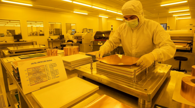
Lamination Precision and Registration Accuracy
Lamination: The act of gluing all the layers of a multilayer PCB by heat and pressure. The prepreg resin is a flowing liquid that flows into the cracks and solidifies to create a solid dielectric. This step will directly influence the values of your final dielectric thickness and impedance.
Normal lamination parameters are:
- Ramping the temperature to 170-185 degrees Celsius based on the resin system.
- Application of pressure 250-400 PSI to provide uniform bonding.
- Curing time of 60-90 minutes at maximum temperature.
- Regulated cooling to reduce thermal stresses and warpage.
Registration accuracy is a measure of the accuracy with which each layer is registered with the rest. The registration is usually between 2 and 3 mils in the case of standard multilayer PCBs. In HDI designs using microvias, registration with tighter tolerances (1 mil or less) is necessary. Misalignment of via-to-pad and impedance variations can be due to poor registration.
Ensuring Uniform Thickness and Void-Free Results
The dielectric thickness must be uniform to achieve uniform impedance in the board. Variations in thickness are caused by a number of factors:
1.Copper density change: Thick copper regions have less resin flow space, leading to local thickness variations. This is counteracted by copper balancing on all layers.
2.Resin starvation: The lack of resin in the prepreg causes gaps and delamination. Prepreg with sufficient resin content should be used in your copper distribution.
3.Press uniformity: Modern presses are vacuum lamination presses, and they prevent the formation of air bubbles and provide uniform pressure throughout the panel.
The IPC-6012 (Qualification and Performance Specification of Rigid PCBs) establishes tolerances of acceptable dielectric thickness of various classes of boards. In the case of Class 2 (dedicated service) boards, tolerance usually is within the range of plus or minus 10 percent. In the case of Class 3 (high reliability), tighter tolerances are used, and manufacturers need to be able to demonstrate the capability based on cross-sectional analysis.
JLCPCB's Expertise in Advanced PCB Stackup Fabrication
Wide Range of Stackup Options and Material Support
JLCPCB offers PCB stackup designs of simple 2-layer to complex multilayer designs, with material selections of standard FR4 and high-frequency laminates such as Rogers in RF applications. JLCPCB offers pre-defined stackup selections, including dielectric thicknesses and Dk values that are documented in the stackup, when controlled impedance is required by the designer. These standard stackup details are available in their ordering platform, where you can access them without having to guess at all when designing the PCB stackup.
DFM Feedback for Optimal High-Speed Performance
JLCPCB's DFM (Design for Manufacturability) review checks your Gerber files and stackup specifications before production begins, catching potential issues such as:
- Dielectric spacing that may not achieve the requested impedance
- Layer arrangements that could lead to warpage or registration problems
- Via structures that conflict with the chosen stackup construction
- Copper distribution imbalances that might cause thickness variation
Getting this feedback before fabrication saves both time and money. It is far better to adjust a dielectric thickness in your design files than to discover an impedance failure after receiving your boards.
Consistent Quality from Prototype to Volume Production
The same process controls and material specifications are upheld by JLCPCB in both small and large production volumes, a single prototype panel or a large production run. PCBs can be as cheap as $2, and can be produced within 1 to 2 days, so you can rapidly run through iterations without sacrificing their stackup quality. When EasyEDA designers utilize the JLCPCB manufacturing platform, it forms an unbroken workflow. It is possible to define your stackup, route your board, and generate production files all in one ecosystem, minimizing the chance of miscommunication between design intent and fabrication execution.
FAQ about PCB Stackup
Q: What is a PCB stackup, and why does it matter?
A PCB stackup is the arrangement of copper layers, dielectric materials (core and prepreg), and solder mask that make up a multilayer circuit board. It directly determines impedance control, signal integrity, power delivery performance, EMI behavior, and mechanical reliability of the finished board.
Q: How many layers do I need for my design?
A simple microcontroller board may only need 2 layers. Designs with controlled impedance requirements, such as USB 3.0 or DDR4 interfaces, typically need at least 4 layers. Complex designs with multiple high-speed buses or high pin-count BGAs often require 6, 8, or more layers.
Q: What is the difference between core and prepreg in a stackup?
Core is a cured laminate with copper foil bonded on both sides, rigid with a precisely known thickness. Prepreg is a semi-cured (B-stage) fiberglass sheet that flows and cures under heat and pressure during lamination to bond cores together. The final thickness of prepreg can vary slightly depending on the surrounding copper density.
Q: How do I achieve controlled impedance in my stackup?
Specify the target impedance (such as 50 ohms single-ended or 100 ohms differential) on your fabrication drawing. Use an impedance calculator during design to choose appropriate trace widths, then let the manufacturer fine-tune dielectric thickness to meet those targets within tolerance.
Q: Can I mix different materials in a single stackup?
Yes, hybrid stackups are common in RF and high-speed designs. A typical example is a Rogers core for the top signal layers combined with standard FR4 for the remaining layers. However, mixed-material stackups require careful CTE (Coefficient of Thermal Expansion) matching to avoid reliability issues during thermal cycling.
Q: What is the 20H rule, and does it still apply?
The 20H rule recommends that the ground plane should extend at least 20 times the dielectric height (H) beyond the power plane edge to reduce fringing field radiation. While its effectiveness is debated in modern high-speed design, keeping ground planes larger than power planes remains a good practice for minimizing edge radiation.
Conclusion
Keep Learning
Building Reliable High-Speed Performance with Effective Timing Analysis
Key Takeaways Timing analysis is essential for high-speed PCBs — clean signals can still fail if they miss setup or hold windows. Focus on setup time, hold time, clock skew, and propagation delay to ensure reliable data sampling. Prioritize length matching, controlled impedance, and proper stackup to maintain positive timing margins. Combine static timing analysis with dynamic simulation for best results. Precision manufacturing is critical — small variations in impedance or dielectric thickness can d......
Low Loss PCBs : Advanced Materials for Superior High-Speed Signal Performance
Key Takeaways Low Loss PCBs using advanced materials like Rogers RO4003C, RO4350B, and PTFE laminates deliver superior signal integrity by dramatically reducing dielectric loss at multi-gigahertz frequencies. Ideal for 5G, mmWave, RF, and high-speed digital designs, these boards offer significantly lower insertion loss, stable impedance, and better thermal performance compared to standard FR4. By choosing the right low-loss laminate and partnering with experienced manufacturers like JLCPCB, engineers ......
How to Reduce Insertion Loss for Better High-Speed PCB Performance
Key Takeaways Reducing insertion loss is essential for achieving reliable high-speed PCB performance. By selecting low-loss materials with lower Df, optimizing trace routing and stackup design, minimizing via transitions, using smoother copper foils, and applying precision manufacturing techniques, designers can significantly lower both dielectric and conductor losses. These strategies help maintain better signal integrity, wider eye openings, and higher data rates in multi-gigabit designs. Have you e......
How to Create the Perfect PCB Stackup for High-Speed and Reliable Designs
Key Takeaways A well-designed PCB stackup is the foundation of high-speed, reliable designs, determining signal integrity, controlled impedance, and EMI performance. Use symmetrical layers with adjacent reference planes, proper dielectric spacing, and copper balancing to avoid warpage and crosstalk. Choose standard FR4 for <3 GHz or low-loss materials (Megtron 6, Rogers) for higher speeds, and work closely with manufacturers for optimal results. Mastering your stackup is essential for high-speed succe......
Achieving Reliable High-Speed Performance with PCB Transmission Lines
Key Takeaways PCB Transmission Lines are essential for reliable high-speed PCB performance in USB 3.0, PCIe, DDR4, and RF designs, turning traces into controlled-impedance structures that eliminate reflections, crosstalk, and attenuation. Select microstrip, stripline, or GCPW geometries with accurate calculations, continuous reference planes, mitered bends, and 3W spacing, then rely on precise etching, copper profile control, and TDR testing at JLCPCB for consistent results from prototype to volume pr......
Backdrill Vias: Enhancing Signal Integrity in High-Speed PCBs
Key Takeaways Backdrill vias remove unused copper stubs from plated through-hole vias, shortening the residual stub to under 0.15 mm (6 mils). This eliminates impedance discontinuities, reflections, and resonances in high-speed signals above 5–10 Gbps. It delivers better return loss, insertion loss, lower jitter, and clearer eye diagrams — all while keeping simple stack-ups and far lower cost than blind/buried vias. Use backdrilling for any stub longer than 15 mils (0.381 mm), especially on boards thi......