Solder Paste Layer: How to Create and Optimize It
13 min
- Quick Answer: What Is the Solder Paste Layer?
- Paste Mask vs Solder Mask: Don't Confuse Them
- How the Solder Paste Layer Becomes Your Stencil
- How to Generate the Solder Paste Layer (KiCad, Eagle, Altium, EasyEDA)
- Optimizing the Solder Paste Layer
- Common Solder Paste Layer Mistakes
- FAQs About the Solder Paste Layer
- Conclusion: Get Your Solder Paste Layer Right
While designing a PCB, you've probably noticed two layers in your EDA tool that look almost identical: the solder paste layer and the solder mask. Both sit alongside the copper layers and use pad-shaped outlines, making it easy to assume they serve the same purpose. They don't, and knowing the difference matters for how your board gets assembled.
This guide breaks down the solder paste layer (a.k.a. cream layer) — what it is, how it differs from the solder mask, how to generate it, and how to optimize its apertures for clean, consistent joints. For the complete set of files required for PCB assembly, see our guide on Files Needed for PCB Assembly.
Quick Answer: What Is the Solder Paste Layer?
The solder paste layer is the PCB design layer that provides the data used to generate the stencil apertures, which determine where solder paste is deposited on the PCB pads before reflow. In the Gerber package, this layer is typically exported as the GTP (Top Paste) and GBP (Bottom Paste) files.
GTP and GBP are just Protel-style file extensions, and the data inside them still follows the Gerber format specification maintained by Ucamco, the same specification used for your copper, solder mask, and silkscreen layers.
Key takeaways
-
It's a positive layer — shapes mark where paste goes, not where copper is exposed.
-
It is used to manufacture the solder paste stencil, not the PCB itself.
-
It is not the solder mask — the solder paste layer controls where solder paste is deposited, while the solder mask controls where copper is exposed.Without a paste layer, no stencil apertures can be generated.
-
Paste apertures are often equal to or slightly smaller than the PCB pads to improve solder paste release and reduce solder defects.

Solder paste layer apertures shown in a Gerber viewer
Paste Mask vs Solder Mask: Don't Confuse Them
Although the two layers may look similar in a PCB design tool, the core distinction comes down to polarity and purpose. The solder mask (GTS on top, GBS on bottom) is a negative layer — its shapes define where the green (or other colored) coating is removed so copper is exposed for soldering. The paste mask, i.e., the solder paste layer (GTP/GBP), is a positive layer — its shapes define where paste is actually printed, and that data is what a stencil is made from.
A side-by-side comparison makes the difference concrete:
| Attribute | Solder Mask (GTS / GBS) | Solder Paste Layer (GTP / GBP) |
|---|---|---|
| Purpose | Protects copper and exposes pads for soldering | Defines where solder paste is deposited before reflow |
| Polarity | Negative — the opening reveals copper | Positive — the shape itself is the paste deposit |
| Gerber files | GTS (top), GBS (bottom) | GTP (top), GBP (bottom) |
| Physical Output | Defines the openings etched into the solder resist coating | Provides the aperture data used to fabricate stencil openings |
| Size vs. pad | Usually equal to or larger than the pad (mask expansion) | Usually equal to or smaller than the pad (aperture reduction) |
| Manufacturing Stage | PCB fabrication | SMT assembly |
Mixing up these two has a direct consequence: send a manufacturer your solder mask data by mistake instead of your paste layer, and the resulting aperture data won't match what your board needs — leading to improper paste deposition, missing apertures, or a stencil that has to be re-cut.
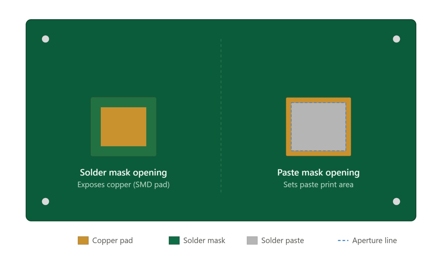
Solder mask vs. paste mask opening
How the Solder Paste Layer Becomes Your Stencil
After you export your Gerber package, the solder paste layer stops being just another design layer and becomes manufacturing data for stencil fabrication. Every aperture defined in the GTP (Top Paste) or GBP (Bottom Paste) file is paste-opening data that a stencil manufacturer processes and translates into a physical opening, typically laser-cut into thin stainless-steel foil. During assembly, a squeegee spreads paste across the finished stencil, forcing it through those openings onto the pads below.
This is why getting the paste layer right matters more than you realize: ordering a stencil is essentially uploading this one file. There's no separate design step at the stencil house — the aperture data you provide is what gets cut, possibly refined by the fabricator's own stencil opening-process standard. Errors in the paste layer become errors in the physical stencil.
Preparing a solder paste layer for a stencil is mostly about getting the aperture geometry right first — after that, selecting the stencil thickness, framing, and finish is the quicker part. Manufacturers such as JLCPCB offer a range of stencil options to suit everything from prototype builds to high-volume production, but the quality of the final stencil still depends on a well-prepared solder paste layer.
How to Generate the Solder Paste Layer (KiCad, Eagle, Altium, EasyEDA)
KiCad
In the PCB editor, go to File > Plot, set the plot format to Gerber, and check F.Paste and B.Paste alongside your copper and mask layers. Enabling "Use Protel filename extensions" only affects file naming — it doesn't change which layers get plotted — but it makes KiCad write these out as .gtp and .gbp, a naming convention widely recognized across the industry.
KiCad's own documentation notes these paste layers exist specifically for stencil manufacturing, not bare-board fabrication. For the full walkthrough, see our KiCad Gerber and drill file generation guide.
Eagle
In Eagle, the solder paste layer is referred to as the Cream Layer. When generating manufacturing files, open the CAM Processor, select the tCream (Layer 31) for the top side or bCream (Layer 32) for the bottom side, and export them using the Gerber RS-274X format. These Gerber files are commonly renamed or exported as GTP and GBP before being sent to the stencil manufacturer.
Altium Designer
Go to File > Fabrication Outputs > Gerber Files, and in the Layers tab select Top Paste and Bottom Paste along with your other layers. Altium exports these as.GTP and .GBP by default, which is the same Protel-style naming most fabricators expect. Altium's fabrication data documentation groups this under its own "Paste Mask" category, separate from Solder Mask — a clear cue it's a distinct file.
EasyEDA
Go to Fabrication > PCB Fabrication File (Gerber). A standard export automatically includes the paste mask layers. Recent EasyEDA versions typically name these as Gerber_TopPasteMaskLayer.GTP and Gerber_BottomPasteMaskLayer.GBP, though exact naming can shift between versions. If you switch to custom export and leave the paste mask layer unchecked, the entire layer is dropped from the zip — worth double-checking before you send files off. See our EasyEDA Gerber generation guide for the full file list.
A couple of habits save real headaches later:
• Always include the paste layer in your Gerber zip when you're ordering a stencil.
• Before sending the Gerber file, open and confirm that the paste apertures actually sit over the correct pads.
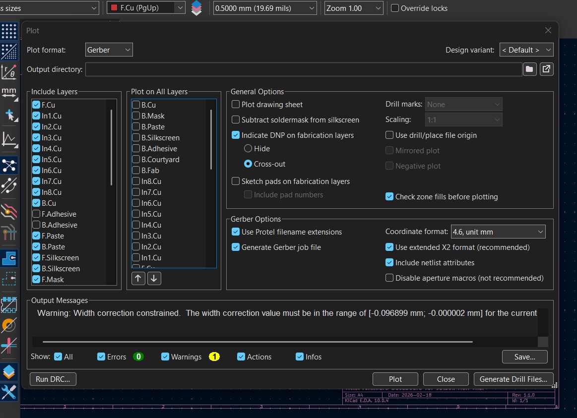
Exporting the F.Paste solder paste layer in KiCad
Choose from Framed/Frameless, Electropolishing, Nano-coating, Step-Stencils, SMD Glue Stencil and more. Starting at $3. No MOQ. 12-Hour production.
Get $11 Coupon Now >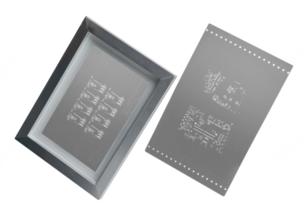
Optimizing the Solder Paste Layer
Aperture Reduction for Fine Pitch
For discrete passive components and fine-pitch ICs, the stencil apertures must be smaller than their matching copper pads. Reducing the aperture area limits the amount of paste applied, preventing excess material from squeezing outward under the component body and causing solder bridges.
According to IPC-7525 (Stencil Design Guidelines), successful paste release depends on two basic design considerations: the aperture's width relative to the stencil thickness (aspect ratio) and the aperture opening area relative to its wall area (area ratio). If these ratios are too small, solder paste may remain inside the stencil aperture instead of transferring cleanly onto the PCB pad. In practice, fine-pitch components often use approximately 10–20% aperture area reduction, although the exact reduction method and amount depend on the component package, pitch, stencil thickness, and the manufacturer's design guidelines. For detailed recommendations, refer to IPC-7525 before finalizing fine-pitch stencil apertures.
Window-Pane for Thermal Pads
Large continuous copper zones, like the exposed center ground pads on QFNs, DFNs, or power MOSFETs, present unique manufacturing challenges. Leaving the paste layer as a massive 1:1 block causes the component to float during reflow and increases solder voids beneath the thermal pad. The fix to this is to divide the paste aperture into a window-pane pattern that covers roughly 50–70% of the copper area. This distributes the solder more evenly while maintaining good thermal contact and improving assembly reliability. For a deeper understanding of thermal pad layout, see our guide on solder pad design.
Through-Hole Pads and Pin-in-Paste
Through-hole pads are not automatically included in the solder paste layer. For Pin-in-Paste (PiP) assembly, dedicated paste apertures must be added explicitly, or they won't appear in the stencil. By default, JLCPCB's CAM process only cuts apertures for pads that already carry paste-layer data; through-hole pad copper and drill layers alone are simply skipped. Check JLCPCB's stencil opening-process standard to see exactly how default aperture rules are applied, since defaults vary between vendors.
Or Let the CAM Optimize It for You
Stencil manufacturers don't just cut each aperture exactly as it appears in the Gerber file. Experienced manufacturers typically run a CAM (Computer-Aided Manufacturing) review before production, evaluating aperture sizes, shapes, and spacing against proven stencil design rules to improve print quality and reduce assembly defects.
At JLCPCB, the CAM process applies its stencil opening-process standards before manufacturing, optimizing paste release instead of reproducing every aperture as a direct 1:1 copy of the pad. Combined with precision laser cutting (±0.003 mm), optional electropolishing, and nano-coating, this produces stencils with cleaner aperture walls and more consistent paste release. To fine-tune this yourself before submitting, see our guides on how to choose a solder paste stencil and SMT stencil design tips, which cover the practical tradeoffs in more depth.
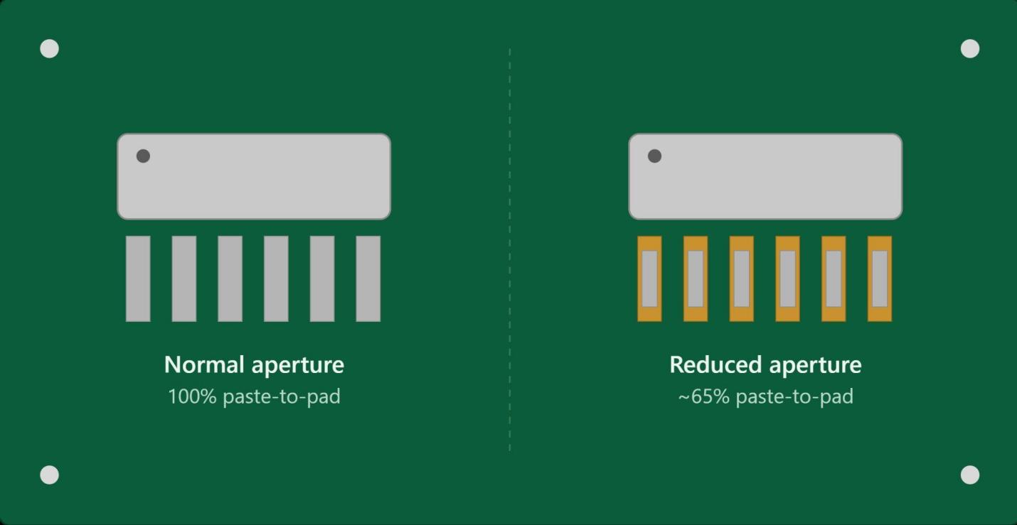
Reduced paste aperture on fine-pitch footprint
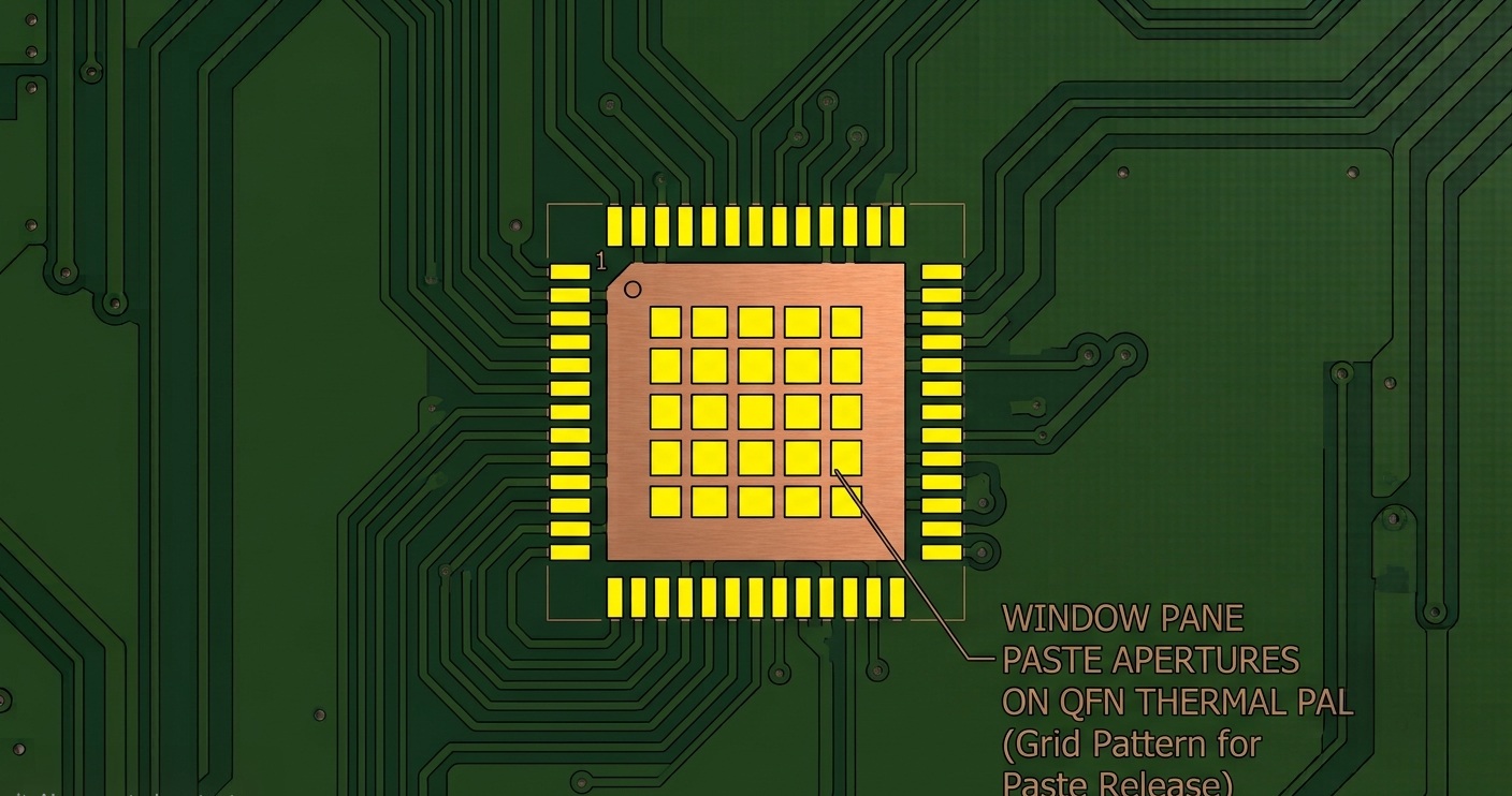
Window-pane paste aperture on a QFN thermal pad
Common Solder Paste Layer Mistakes
Solder paste printing defects like bridging or tombstoning at reflow are mostly caused by a few common mistakes. Check your design against these common oversights before sending your files:
-
No paste layer exported:
Results in no stencil apertures cut. Always include and verify both Top and Bottom Paste layers when exporting Gerber files.
-
Apertures left 1:1 with pads on fine pitch:
Leads to excessive paste volume and severe solder bridging during reflow. Ensure reductions are applied manually or handled via manufacturing CAM systems.
-
Through-hole pads left off the paste layer:
Those holes never get cut for pin-in-paste assembly; add them explicitly.
-
Paste printed over open vias:
Liquid solder will wick down into untented via structures, leaving the primary landing pad starved of solder. Keep paste off open vias or ensure they are tented with a solder mask.
-
Confusing the paste layer with the solder mask:
Yields completely incorrect stencil openings or missing stencils entirely. Double-check all layer bindings inside a standalone Gerber viewer before submission.
FAQs About the Solder Paste Layer
Does every PCB need a solder paste layer?
Not always. A solder paste layer is required only when a PCB will be assembled using surface-mount technology (SMT) and a solder paste stencil. Boards built entirely with through-hole components typically don't require a paste layer unless they use Pin-in-Paste (PiP) assembly techniques.
Can I request aperture changes after I've already sent my Gerber files to a fabricator?
It depends on the manufacturing stage. If the stencil hasn't entered production yet, many manufacturers can review your request and, in some cases, apply aperture modifications during the CAM review or ask you to provide updated Gerber files. Once the stencil has been laser-cut, aperture changes are not possible, and a new stencil will usually be required.
What is the standard thickness for a solder paste stencil?
The standard thickness for most multi-purpose SMT stencils ranges between 0.10 mm and 0.15 mm (4 to 6 mils). Selecting the correct thickness requires balancing your components' needs: ultra-fine-pitch ICs require thinner stencils (0.08 mm / 3 mils) to prevent bridging, while larger power components need thicker stencils to deposit enough paste volume for a secure mechanical joint.
Should I order a framed or frameless stencil for my paste layer?
It depends on how you'll assemble the PCB. Frameless stencils are a cost-effective choice for prototypes, low-volume production, or manual solder paste application, especially when used with a stencil holder or reusable frame. Framed stencils are better suited for medium- to high-volume production because they provide improved rigidity, alignment, and compatibility with automatic stencil printers.
Can a stencil manufacturer modify my paste layer?
Many stencil manufacturers perform a CAM review before production and may apply standard aperture optimizations. However, the quality of the final stencil still depends on the Gerber data you provide, so it's always good practice to review and verify the solder paste layer before submitting it for manufacturing.
Should through-hole pads appear on the paste layer?
Only if you're using pin-in-paste (PiP) reflow, where through-hole components are soldered in the same reflow cycle as SMT components. For conventional through-hole assembly, leave those pads off the paste layer; including them by accident just wastes paste and risks flux residue in the barrel.3
Conclusion: Get Your Solder Paste Layer Right
The solder paste layer is the bridge between your design and a clean SMT print: it is not the solder mask; it needs to be generated and verified carefully, and its apertures deserve the same attention that you give to the trace widths or clearances. Get the shapes and sizes right, verify the file in a Gerber viewer, and the rest of the process will go much more smoothly.
Once that file is correct, ordering a stencil is genuinely just an upload away. And you'll be one step closer to a smoother, more reliable SMT manufacturing process.
Keep Learning
BGA Stencil Design: Apertures, Thickness & Tips
On a ball grid array, every solder joint hides underneath the package where you cannot see it, touch it, or easily rework it. That is exactly why BGA stencil design decides whether the board works: the paste you print is the paste you get, and a print that is slightly too heavy or too light turns into hidden bridges, voids, or starved balls that only an X-ray will reveal. Get the stencil right and the joints reflow clean the first time. Get it wrong and you are chasing intermittent faults after assemb......
Stencil Aperture Design: Geometry, Area Ratio & Tips
Key Takeaways Stencil aperture design controls paste volume, deposit shape, and print registration — it's the key controllable variable in SMT print quality. As per IPC-7525B, two math rules are non-negotiable: stencil area ratio ≥ 0.66 and stencil aspect ratio ≥ 1.5. Aperture geometry is component-dependent: 1:1 with pad for BGA, window-pane splits for QFN/BGA thermal pads, home-plate shapes for 0201/01005 chips, and modest reductions for fine-pitch QFP. Aperture reductions intentionally decrease the......
Red Glue Stencil: Types, Thickness & Ordering Guide
Key Takeaways A red glue stencil deposits adhesive dots under component bodies, not solder paste on electrical pads. Its main use is holding bottom-side SMD parts during wave soldering of through-hole leads. SMT red glue is commonly dyed red so operators can confirm each deposit during inspection. Printable adhesive families include epoxy, acrylic, and UV- or dual-cure materials. Glue stencils are commonly thicker than paste stencils because the dot must reach the component underside. A custom o......
DFN Package Guide: Footprint, Soldering & Stencil Tips
Key Takeaways What a DFN is: A DFN (Dual Flat No-Lead) package is a leadless chip-scale IC package with connection pads on two opposing sides of its underside, usually plus a central exposed thermal pad. Assembly requirements: DFN joints sit hidden under the body, so it needs reflow soldering with a stencil and X-ray or AOI inspection, not hand soldering. Design essentials: Follow IPC-7351 land patterns and IPC-7525 aperture rules, use a thinner stencil foil around 0.1-0.12 mm, and segment the thermal......
A Beginners Guide to Step-Up and Step-Down Stencils
As everyone knows, companies are moving down to 2nm, and electronics are at their peak right now. The component sizes of a PCB likewise drastically shrink during a ten-year period. From 1206, BGAs have shrunk to 0402, 0201, and even smaller. Due to the small size of the components and the requirement for high throughput, defects such as tombstoning, bridging, or poor connections may occur during the soldering process. To address these challenges, specialized stencil technologies such as step-up and st......
Design Guidelines for Industry-Standard Solder Stencil
Solder paste printing is one of the most important processes in PCB assembly, and the design of a stencil directly affects the quality of solder paste application. In a previous article, we discussed stencils and their types in detail. JLCPCB’s advanced stencil options, including step-up/step-down and nano-coated stencils, help engineers achieve higher printing accuracy and assembly reliability. In electronics hardware design, following proper design rules is just as crucial as having the right tools.......