Red Glue Stencil: Types, Thickness & Ordering Guide
11 min
- What Is a Red Glue Stencil?
- When to Use a Red Glue Stencil
- Why Red Glue Is Less Common in Modern SMT Assembly
- How to Customize a Red Glue Stencil for Your Board
- Types of SMT Glue That Can Be Printed Through a Stencil
- How to Order a Red Glue Stencil From JLCPCB
- Specifying a Custom Red Glue Stencil: A Procurement Checklist
- FAQ about Red Glue Stencils
- Conclusion: Treating Red Glue Stencil Selection as a Process Decision
Key Takeaways
A red glue stencil deposits adhesive dots under component bodies, not solder paste on electrical pads.
Its main use is holding bottom-side SMD parts during wave soldering of through-hole leads.
SMT red glue is commonly dyed red so operators can confirm each deposit during inspection.
Printable adhesive families include epoxy, acrylic, and UV- or dual-cure materials.
Glue stencils are commonly thicker than paste stencils because the dot must reach the component underside.
A custom order is defined mainly by foil thickness, aperture geometry, frame format, and surface treatment.
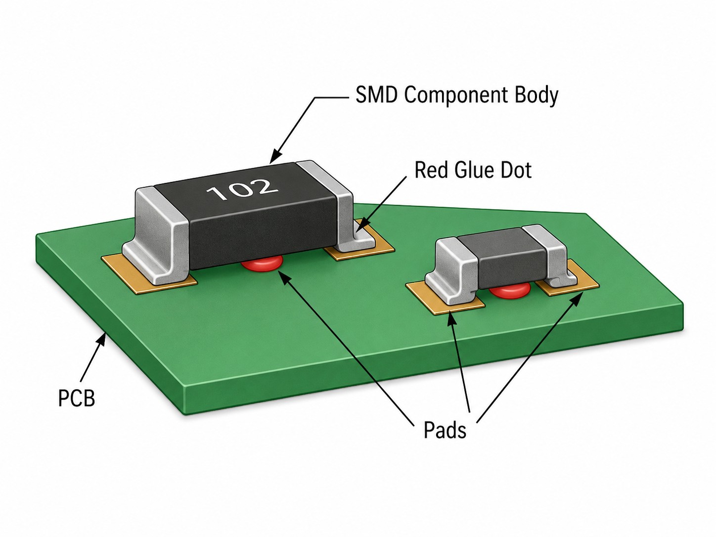
In mixed-technology assembly, bottom-side SMD components may reach wave soldering before any solder joint has formed. Without a mechanical anchor, the moving solder wave can shift or remove them. A red glue stencil prevents this by printing controlled adhesive dots under the component bodies before placement and curing.
"Red glue" is the workshop name for SMT-grade epoxy adhesive (what the industry calls SMT glue), usually dyed red for visual inspection. The stencil itself is a precision-cut metal foil, not a red-coated tool. This guide explains when it is needed, how to specify it, what adhesive it handles, and how to order one.
What Is a Red Glue Stencil?
A red glue stencil is a laser-cut foil that deposits surface mount adhesive at selected PCB locations. Its openings sit between or beside the pads, so cured glue contacts the package underside without contaminating solderable surfaces.
"Red" refers to the adhesive color used for inspection; equivalent circuit board adhesive may be blue, yellow, or clear. Terms such as "SMT glue stencil" "surface mount adhesive stencil" and "glue for PCB components" describe the same application.
JLCPCB uses 304 HTA stainless steel for custom laser-cut stencils and supports both solder-paste and adhesive applications.
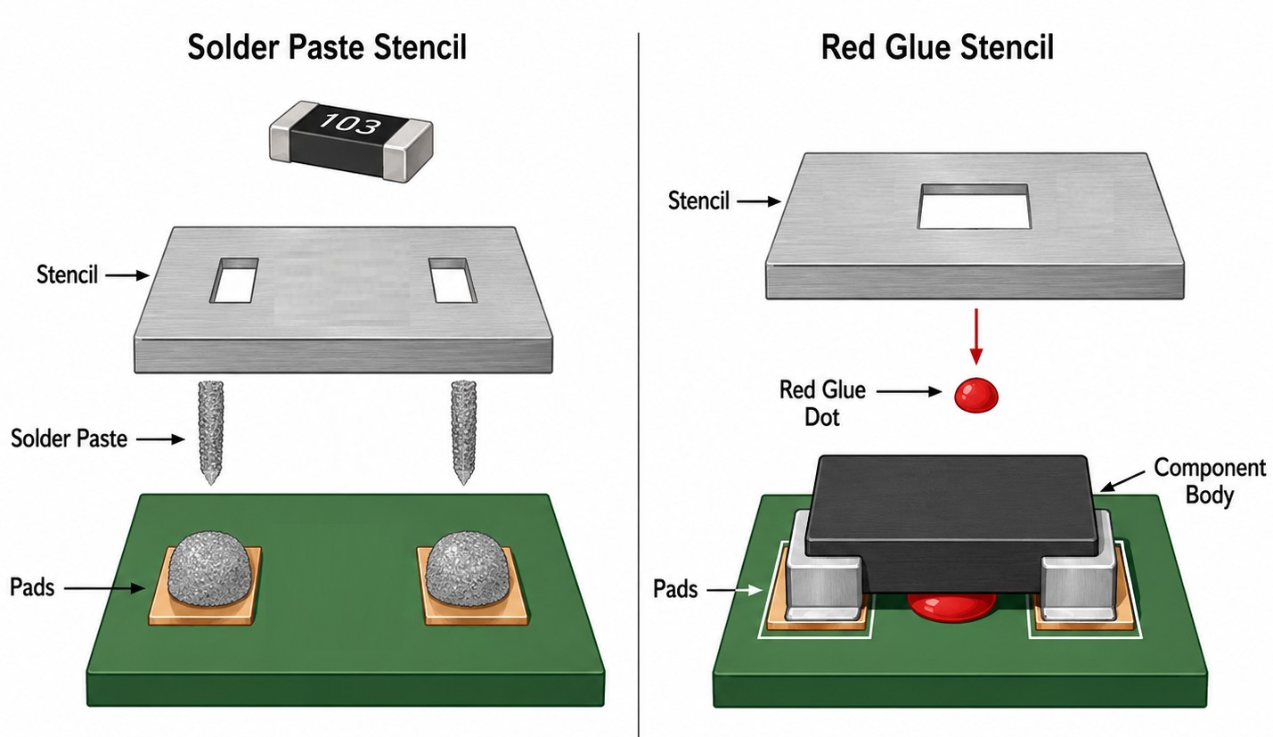
How a Red Glue Stencil Differs From a Solder Paste Stencil
| Aspect | Solder Paste Stencil | Red Glue Stencil |
|---|---|---|
| What It Deposits | Solder paste for electrical and mechanical joints | Non-conductive component adhesive |
| Foil Thickness | Commonly 0.10–0.15 mm | Commonly 0.15–0.30 mm |
| Aperture Logic | Based on pad geometry and paste volume | Based on glue-dot size, count, and position |
| Deposit Location | Directly on PCB pads | Under the component body, away from pads |
| Next Process | Placement and reflow | Placement, cure, and wave soldering |
Mixed-technology production may need both: a paste stencil for reflow and a glue stencil for wave-bound parts. Ordering both stencils from a single Gerber upload guarantees pad-perfect alignment between the two foils. For printing and curing, see How to Apply SMD Glue Using SMT Stencils.
When to Use a Red Glue Stencil
Use red glue only when the assembly route requires it.
Use Cases Where a Red Glue Stencil Earns Its Cost
- Bottom-Side SMD on Wave-Soldered Boards: Adhesive prevents parts from shifting or washing away.
- Mixed SMD and Through-Hole Assemblies: Leaded parts may require a later wave process after SMD placement.
- High-Volume Runs: Above roughly 500 boards per cycle, stencil printing can remove dispensing bottlenecks.
- Tight Dot-Volume Control: A stencil supports repeatable deposits and tight volume control.
- Shock- or Vibration-Sensitive Products: Adhesive can add mechanical support where the environment justifies it.
When a Different Glue Application Method Is Better
| Method | Best For | Volume Fit | Trade-Off |
|---|---|---|---|
| Stencil Printing | Stable designs with many uniform dots | Medium to high | Custom tooling required |
| Time-Pressure or Jet Dispensing | Frequent changes or varied dot sizes | Low to medium | Flexible but slower per board |
| Manual Syringe | Prototypes, repair, and tiny batches | Very low | Lowest consistency |
Red glue stencils sit in the sweet spot of medium-to-high volume, uniform component standoff, and consistent dot-volume needs. Outside those conditions—for prototypes, frequent design changes, or mixed standoff heights—dispensing or manual application is often more economical.
Why Red Glue Is Less Common in Modern SMT Assembly
Many factories now reflow both PCB sides, so bottom-side parts form joints before later processing and do not need glue to survive a full wave. Selective soldering targets only remaining through-hole leads, keeping nearby SMD components away from molten solder. Pin-in-paste and the declining use of through-hole parts reduce glue demand further, especially in consumer electronics.
However, mixed PCB assembly still needs adhesive when bottom-side SMD parts pass over a wave. It also remains useful in high-volume lines and vibration-sensitive industrial or automotive products—where thermal cycling and mechanical shock demand a bond beyond the solder joint alone. Review the complete SMD vs THT assembly route before deciding.
How to Customize a Red Glue Stencil for Your Board
Four parameters control most custom orders: foil thickness, aperture geometry, frame format, and surface treatment.
Foil Thickness
Thickness controls deposit volume and height. A useful starting rule is a dot around 1.5–2 times the component standoff, then validation with the adhesive supplier and a print trial.
Typical thickness is 0.15–0.30 mm: about 0.15 mm for low-standoff chips, 0.18 mm for many SOT/SOIC packages, 0.20–0.25 mm for higher standoffs, and 0.30 mm for large packages or connectors. A step stencil can provide different heights on one board.
Aperture Geometry for Glue Dots
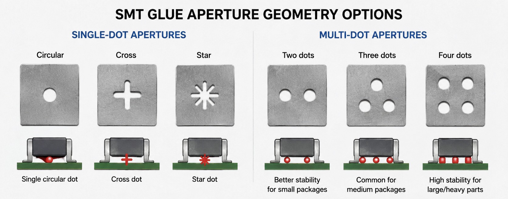
Glue apertures follow the component body, not the copper pads. Small chips may use one central dot; SOICs, QFPs, and connectors may use multiple dots to resist rotation.
A common starting diameter is 50–70% of body width. Too little glue may fail under wave force; excess can squeeze toward the leads. Circular apertures are common, while cross or star shapes can control spread.
Never place glue on solder pads: cured adhesive is insulating and can block wetting. JLCPCB publishes red glue opening rules, while its stencil design guide explains material transfer.
Frame Format: Framed vs Frameless
Framed stencils suit automatic or semi-automatic printers. Frameless foils cost and weigh less, fitting prototypes, small batches, or reusable frames. Select by printer hardware and working area; a custom stencil maker can confirm dimensions.
Surface Treatment Options
Electropolishing smooths aperture walls for better release. Nano-coating reduces foil adhesion and is often worthwhile for runs above 100 boards or viscous glue. For frequent ultrasonic cleaning, choose ultrasonic-resistant frame bonding. Match treatments to aperture size, adhesive, cleaning method, and volume.
Types of SMT Glue That Can Be Printed Through a Stencil
The stencil controls geometry; the SMT glue controls cure, strength, heat resistance, and storage. IPC-SM-817 covers dielectric surface-mount adhesives, including stencil-applied products, and classifies them by cure system.
Epoxy SMT Red Glue
Epoxy is the classic SMT red glue for bottom-side wave soldering. It offers high strength and heat resistance. Typical printable grades are thixotropic, around 80,000–400,000 cP, and may cure near 100–150 °C for 1–5 minutes; some require longer post-cure.
Acrylic Surface Mount Adhesives
Acrylic formulations offer fast fixture times and may cure at ambient or moderate temperature. They suit lines where oven time is a bottleneck, but the grade must withstand later soldering and meet electrical-cleanliness requirements.
UV-Curable and Dual-Cure Adhesives
UV-curable materials can reach handling strength in seconds, often using 365 nm light and product-specific doses around 200–500 mJ/cm². Shadowing under opaque parts is the limitation. Dual-cure products add heat, moisture, or chemical curing for hidden adhesive.
Choosing the Right Adhesive for Your Stencil
Printability depends on viscosity, thixotropy, aperture size, and release. Give the supplier the adhesive part number before finalizing thickness, and match its cure profile to available equipment.
How to Order a Red Glue Stencil From JLCPCB
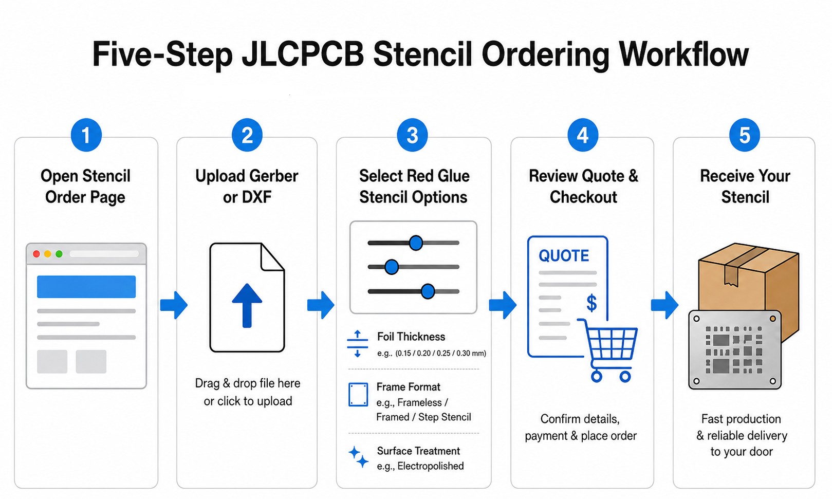
The parameters are similar across suppliers; JLCPCB uses one online workflow for paste and adhesive stencils.
Open the JLCPCB SMT Stencil Page
Use the JLCPCB stencil product page to order with the PCB or as a separate item.
Upload the Gerber or DXF
Include a clearly named adhesive layer and explain special layer naming in the order remarks.
Select the Red Glue Stencil Parameters
Choose foil thickness, framed or frameless format, and treatments such as electropolishing or nano-coating.
Review the Quote and Production Details
JLCPCB lists custom laser-cut stencils from $3 with an MOQ of one.
Confirm the Production File and Place the Order
The fastest listed build time is 12 hours. JLCPCB serves 180+ countries, and express delivery is often around a week, depending on destination and courier.
For mixed-tech boards, order paste and glue stencils from the same PCB origin to reduce layer-offset and alignment errors.
Specifying a Custom Red Glue Stencil: A Procurement Checklist
- Provide a Clearly Labeled Adhesive Layer. Submit a Gerber or DXF showing every glue location. Label the adhesive layer clearly instead of relying on the supplier to derive it from paste data.
- Identify the Adhesive Product. Include manufacturer and part number. This lets the supplier check viscosity, thixotropy, cure profile, and temperature capability.
- Report Important Component Standoffs. Highlight packages above about 0.5 mm standoff or with unusual geometry. Attach the relevant datasheet drawing when dimensions are unclear.
- Select Thickness From Deposit Needs. Base foil thickness on package geometry and adhesive behavior, not on the paste stencil. Ask for a supplier review when uncertain.
- Match the Frame to the Printer. Automatic printers normally need framed stencils. Manual setups often use frameless foils or reusable tensioning frames.
- Choose Treatments Deliberately. Electropolishing and nano-coating can improve release for viscous materials and long runs. They are not mandatory for every design.
- Confirm Lead Time and Shipping. Confirm build time after selecting every option. Advanced finishes, frame size, destination, and courier can change the final schedule.
FAQ about Red Glue Stencils
Q: Can a Red Glue Stencil Be Reused?
Yes. Reuse it for the same PCB revision while the foil remains flat, the apertures are undamaged, and all residue is removed before curing. Store the stencil in a clean, dry cover and protect the aperture area from bending. Inspect fiducials, frame tension, and openings before each run. A layout revision that moves parts or changes glue-dot geometry usually requires a new stencil, even when the PCB outline remains unchanged.
Q: How Should a Glue Stencil Be Cleaned?
Clean it before the adhesive cures inside the apertures. Use only a solvent and method approved by the adhesive manufacturer, because the wrong chemical can leave residue or damage the frame bond. Wipe both sides, then inspect openings against a light source. Before ultrasonic cleaning, confirm that the framed stencil uses an ultrasonic-resistant bonding system and follow the supplier’s cleaning limits.
Q: What Causes Inconsistent Glue Dots?
Typical causes are blocked apertures, poor board support, incorrect squeegee pressure, unsuitable separation speed, or adhesive outside its recommended temperature range. Start by cleaning the stencil and checking PCB-to-stencil contact. Then verify adhesive condition and print settings. If deposits remain incomplete, review aperture geometry, foil thickness, electropolishing, nano-coating, and the adhesive’s storage history.
Q: Can One Stencil Apply Solder Paste and Red Glue?
Normally, no. Paste and adhesive are deposited at different locations and often need different thicknesses. Paste openings sit over copper pads; glue openings sit under component bodies and away from pads. Combining both in one normal stencil creates contamination and process-control risks. Mixed-technology boards usually use one solder-paste stencil and a separate red glue stencil, each generated from its correct manufacturing layer.
Q: Do All Double-Sided PCBs Need SMT Red Glue?
No. Double-sided reflow can solder the first side before the second pass, so adhesive may be unnecessary when component mass and the thermal profile are suitable. Red glue is mainly required when bottom-side SMD parts will face wave soldering before their joints are formed. Review the full assembly sequence before adding a glue step, because it increases material, curing, inspection, and rework effort.
Conclusion: Treating Red Glue Stencil Selection as a Process Decision
A red glue stencil is not a commodity sheet. Thickness controls deposit height, aperture geometry controls volume and location, the frame controls handling, and surface treatment affects release and cleaning.
Select the stencil together with the adhesive, component standoff, soldering route, and production volume. When the stencil is right, the bond is repeatable; when the bond is repeatable, your wave line stops being the stage where components are lost.
Keep Learning
BGA Stencil Design: Apertures, Thickness & Tips
On a ball grid array, every solder joint hides underneath the package where you cannot see it, touch it, or easily rework it. That is exactly why BGA stencil design decides whether the board works: the paste you print is the paste you get, and a print that is slightly too heavy or too light turns into hidden bridges, voids, or starved balls that only an X-ray will reveal. Get the stencil right and the joints reflow clean the first time. Get it wrong and you are chasing intermittent faults after assemb......
Stencil Aperture Design: Geometry, Area Ratio & Tips
Key Takeaways Stencil aperture design controls paste volume, deposit shape, and print registration — it's the key controllable variable in SMT print quality. As per IPC-7525B, two math rules are non-negotiable: stencil area ratio ≥ 0.66 and stencil aspect ratio ≥ 1.5. Aperture geometry is component-dependent: 1:1 with pad for BGA, window-pane splits for QFN/BGA thermal pads, home-plate shapes for 0201/01005 chips, and modest reductions for fine-pitch QFP. Aperture reductions intentionally decrease the......
Red Glue Stencil: Types, Thickness & Ordering Guide
Key Takeaways A red glue stencil deposits adhesive dots under component bodies, not solder paste on electrical pads. Its main use is holding bottom-side SMD parts during wave soldering of through-hole leads. SMT red glue is commonly dyed red so operators can confirm each deposit during inspection. Printable adhesive families include epoxy, acrylic, and UV- or dual-cure materials. Glue stencils are commonly thicker than paste stencils because the dot must reach the component underside. A custom o......
DFN Package Guide: Footprint, Soldering & Stencil Tips
Key Takeaways What a DFN is: A DFN (Dual Flat No-Lead) package is a leadless chip-scale IC package with connection pads on two opposing sides of its underside, usually plus a central exposed thermal pad. Assembly requirements: DFN joints sit hidden under the body, so it needs reflow soldering with a stencil and X-ray or AOI inspection, not hand soldering. Design essentials: Follow IPC-7351 land patterns and IPC-7525 aperture rules, use a thinner stencil foil around 0.1-0.12 mm, and segment the thermal......
A Beginners Guide to Step-Up and Step-Down Stencils
As everyone knows, companies are moving down to 2nm, and electronics are at their peak right now. The component sizes of a PCB likewise drastically shrink during a ten-year period. From 1206, BGAs have shrunk to 0402, 0201, and even smaller. Due to the small size of the components and the requirement for high throughput, defects such as tombstoning, bridging, or poor connections may occur during the soldering process. To address these challenges, specialized stencil technologies such as step-up and st......
Design Guidelines for Industry-Standard Solder Stencil
Solder paste printing is one of the most important processes in PCB assembly, and the design of a stencil directly affects the quality of solder paste application. In a previous article, we discussed stencils and their types in detail. JLCPCB’s advanced stencil options, including step-up/step-down and nano-coated stencils, help engineers achieve higher printing accuracy and assembly reliability. In electronics hardware design, following proper design rules is just as crucial as having the right tools.......