DFN Package Guide: Footprint, Soldering & Stencil Tips
14 min
- Quick Answer: What Is a DFN Package?
- DFN Package Anatomy: Lands, Thermal Pad, and No Leads
- DFN Naming Decoded: SON, WSON, VSON, MLPD, and LLP
- DFN vs QFN: What's the Difference?
- DFN Footprint and Land Pattern Design
- How to Solder a DFN: Why You Need Reflow and a Stencil
- Common DFN Soldering Defects
- DFN Applications and When to Choose a DFN Package
- FAQ about DFN Package
- Conclusion: Designing and Assembling With DFN Packages
Key Takeaways
- What a DFN is: A DFN (Dual Flat No-Lead) package is a leadless chip-scale IC package with connection pads on two opposing sides of its underside, usually plus a central exposed thermal pad.
- Assembly requirements: DFN joints sit hidden under the body, so it needs reflow soldering with a stencil and X-ray or AOI inspection, not hand soldering.
- Design essentials: Follow IPC-7351 land patterns and IPC-7525 aperture rules, use a thinner stencil foil around 0.1-0.12 mm, and segment the thermal-pad aperture into a window-pane grid to keep voiding low.
You've spec'd, or received, a chip in a DFN package: a tiny leadless part with its connection pads hidden underneath the body. Now you need to lay it out and solder it without shorts, opens, or a floating thermal pad.
This guide explains the DFN package end to end: what it is, how it compares to QFN, how to design its footprint, and how to assemble it reliably. For a tour of all SMD IC packages, see our IC package types guide; here we go deep on DFN specifically.
Quick Answer: What Is a DFN Package?
A DFN (Dual Flat No-Lead) package is a leadless, chip-scale surface-mount IC package with connection pads on two opposing sides of its underside, usually plus a central exposed thermal pad. It's compact and thermally efficient, but its joints are hidden, so it needs reflow soldering and X-ray or AOI inspection.
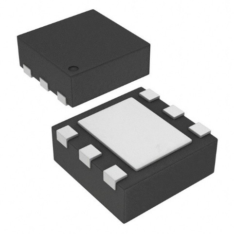
A few things worth knowing up front:
- Lands sit on two opposing sides, not four like QFN.
- Most DFNs include a central exposed thermal pad (EP).
- Low pin counts, but strong thermal and RF performance for the size.
- Not practically hand-solderable; it needs reflow and a stencil.
- Joints are hidden, so X-ray or AOI inspection is standard.
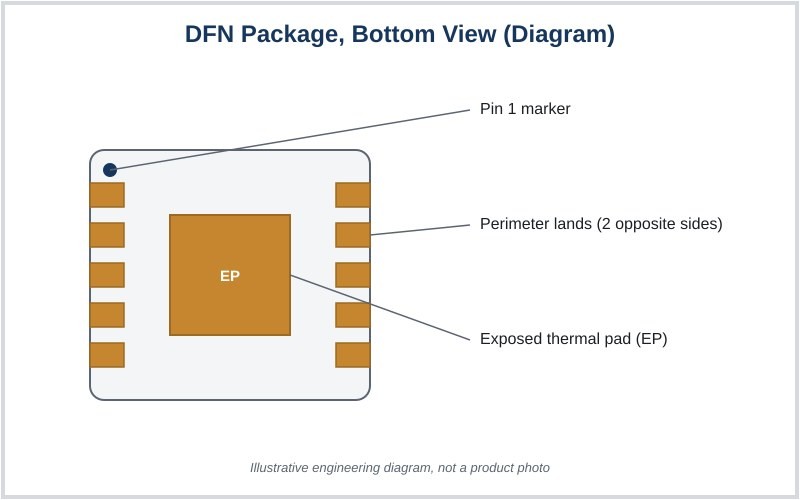
DFN Package Anatomy: Lands, Thermal Pad, and No Leads
Strip away the branding and a DFN is a copper lead frame with a die attached, wire-bonded, and sealed in molding compound. Instead of pins bent out from the sides, the lead frame's perimeter is exposed on two opposite edges as flat lands, sitting nearly flush with the package body.
That construction gives DFN a near-chip-scale footprint and very short internal interconnects, which keeps parasitic inductance low. It's part of why DFN and its relatives show up so often above roughly 100 MHz, in RF front-ends and fast switching regulators, where longer leads would start to matter electrically.
The Exposed Thermal Pad (EP)
Most DFNs, especially DFN-6 and DFN-8 variants used for MOSFETs and LDOs, add a central metal pad on the underside. That pad conducts heat directly from the die into the PCB's copper, rather than relying on the small perimeter lands alone.
It sets up two design questions covered later: how to via it into the board's ground or heat-spreader plane, and how to stencil it without trapping voids. For more on how lands, pads, and other footprint elements fit together, see our SMD Packages Explained guide.
DFN Naming Decoded: SON, WSON, VSON, MLPD, and LLP
Ask five engineers what a DFN really is and you'll get five overlapping answers, because the naming didn't come from one source.
DFN and SON (Small-Outline No-lead) describe the same basic construction; different manufacturers just picked different names. WSON and VSON are the same idea at different package heights.
MLPD (Micro Leadframe Package, Dual) and LLP (National Semiconductor's, later TI's, original name) are two more labels for essentially the same leadless, two-side-land family. MFF2 is a specific DFN-8 variant used for eSIM modules.
JEDEC MO-229 defines the DFN package outline, and JESD75 covers pin assignment conventions, but DFN geometries vary more from vendor to vendor than QFN's do. Whatever the datasheet calls the part, trust its land pattern over any generic template.
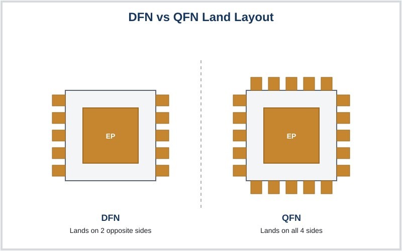
DFN vs QFN: What's the Difference?
The core difference is simple: DFN has lands on two opposite sides, QFN has them on all four. That makes DFN a natural fit for lower pin counts and smaller outlines, while QFN's quad perimeter suits higher pin counts.
Beyond that, assembly rules are nearly identical: both are leadless, both usually carry an exposed pad, and both need reflow soldering rather than an iron.
| Attribute | DFN | QFN |
|---|---|---|
| Lands | Two opposite sides | All four sides |
| Typical pin count | Low to medium | Medium to high |
| Exposed thermal pad | Usually present | Usually present |
| Assembly process | Reflow + stencil, not hand-solderable | Reflow + stencil, not hand-solderable |
Choose DFN over QFN when your pin count is low to medium and a full quad perimeter would just be wasted board space. For the four-side details, see our Ultimate Guide to QFN Package.
DFN Footprint and Land Pattern Design
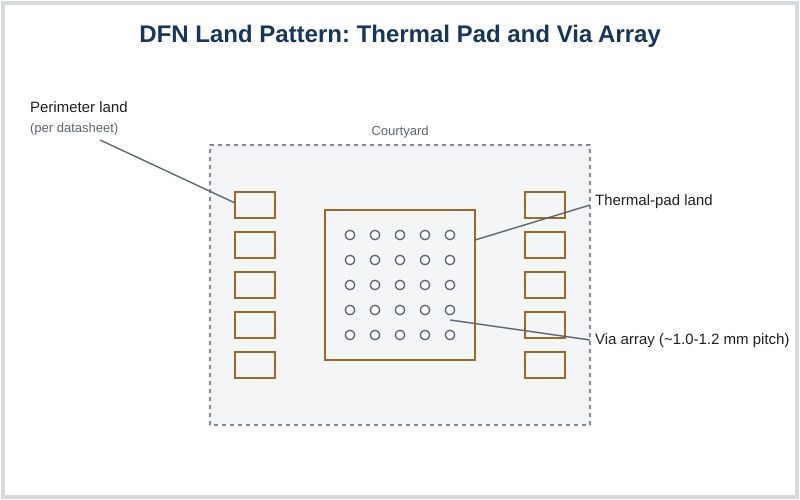
Land pattern basics follow IPC-7351: perimeter land sizing based on the datasheet's terminal dimensions, a courtyard keep-out around the package, and a separate land for the thermal pad.
Thermal Pad and Via Array
Connect the EP to the board's ground or heat-spreader plane with a via array, typically on a 1.0-1.2 mm (39-47 mil) pitch. Tent or plug those vias so solder paste doesn't wick down into them during reflow instead of forming the joint.
SMD vs NSMD Pads
There's a real trade-off in how you define the pad edges.
NSMD (non-solder-mask-defined) pads, where the mask pulls back from the copper, tend to be more reliable under thermal cycling since the copper-to-solder transition sees less stress concentration.
SMD (solder-mask-defined) pads, where the mask overlaps the copper, can reduce bridging risk on very fine pitches, since the mask itself acts as a dam.
For DFN's typical pitches, check IPC-7351 and JEDEC MO-229 guidance and match whichever the datasheet's own land pattern already assumes. Our IC Package Types Guide covers the broader footprint fundamentals this builds on.
Our SMD Packages Explained guide is a good next read if you want the broader SMD footprint conventions this section builds on.
How to Solder a DFN: Why You Need Reflow and a Stencil
Here's the honest reality: a DFN is not practically hand-solderable. The lands sit low and partly hidden under the body, and the exposed thermal pad sits entirely underneath it, so a soldering iron simply can't reach the joints.
Reflow, whether in an oven, on a hot plate, or with hot air, is required, with paste applied by a stencil beforehand. The real question isn't how to hand-solder a DFN. It's how to print and reflow it well.
Stencil Aperture and Thickness for DFN
DFN lands and pitches down to about 0.4 mm (16 mil) need a precise, repeatable paste volume: too little starves the joint, too much bridges neighboring lands.
IPC-7525's aspect-ratio (≥1.5) and area-ratio (≥0.66) guidelines are the basis for sizing apertures that release cleanly at this scale.
What to look for: accurate aperture cutting, since small apertures have little tolerance for edge error, and the right foil thickness. A DFN usually wants a thinner foil, around 0.1-0.12 mm (4-5 mil), so the deposit volume matches its fine lands rather than the thicker foil a coarser-pitch part might use. Our guide on how to choose a solder paste stencil covers this selection in more depth.
Why Paste Release Decides Fine-Pitch DFN
At 0.4-0.5 mm pitch, the limiting factor usually isn't heat. It's whether the printed paste actually releases cleanly from the aperture.
Rough aperture walls hold paste back, leaving starved or inconsistent deposits regardless of how good the reflow profile is.
Clean release comes down to smooth aperture walls plus a low-friction surface. Electropolishing smooths the laser-cut walls and removes micro-burrs, and an optional nano-coating adds a non-stick layer on top. That combination is the general engineering reason fine-pitch DFN prints succeed or fail.
Window-Pane on the Thermal Pad
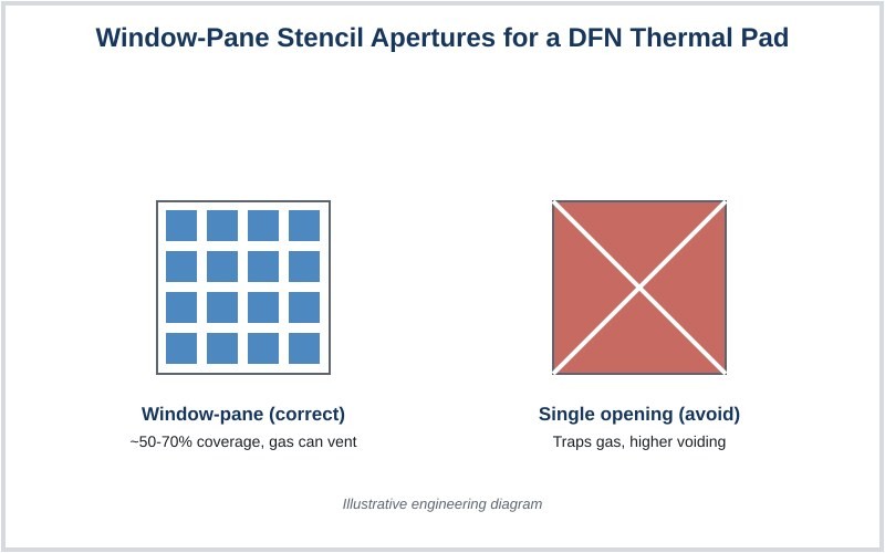
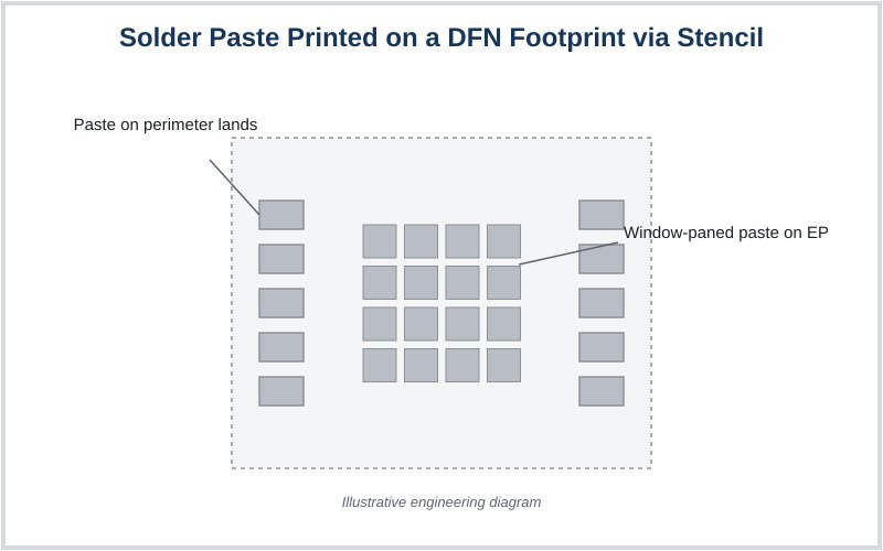
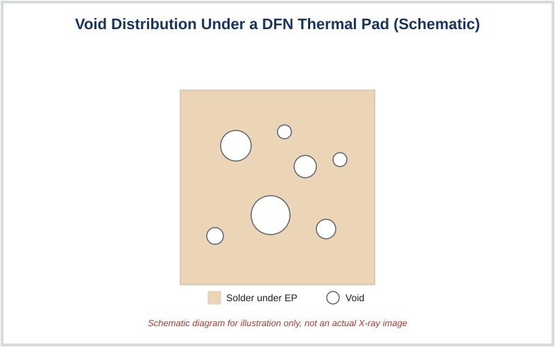
Never print the exposed pad as one big opening. Segment the aperture into a window-pane grid, roughly 50-70% coverage, so flux gas has somewhere to escape during reflow and voiding stays low, ideally under 25%.
Web the stencil over any in-pad vias too, or paste will wick down them instead of staying on the pad.
This pattern has to be defined on the solder paste layer in your design files. Many stencil houses' CAM process will also optimize thermal-pad apertures during file review; see the stencil opening-process standard for how that review works.
Reflow and Inspection
From there it's a standard soak-reflow-cool profile; see our reflow soldering guide for the base mechanics. Because DFN joints sit hidden under the body, inspect with X-ray or AOI rather than a visual check alone.
Texas Instruments' AN-1187 (Leadless Leadframe Package, the successor naming for LLP/DFN) is a useful reference for these steps if you want the assembly guidance straight from a component maker. If building a reliable reflow setup isn't practical for your volume, professional SMT assembly is a reasonable alternative.
Common DFN Soldering Defects
Most DFN soldering problems trace back to one stage: how the paste gets deposited.
| Defect | Root Cause | Fix |
|---|---|---|
| Bridging on fine perimeter lands | Excess paste volume, or apertures too close together | Reduce aperture size; smoother walls; controlled volume |
| Insufficient or open joints | Starved deposits from poor release, or vias wicking paste away | Tent vias; electropolish or nano-coat; correct foil thickness |
| Thermal-pad voiding | A solid EP deposit traps outgassing flux | Window-pane apertures plus an extended soak |
| Floating or skewed part | Too much EP paste lifts the package during reflow | Cut EP paste coverage; keep pad design symmetrical |
Most DFN defects are decided at paste deposition, which the stencil controls. See our guide to solder paste printing defects for patterns that apply across leadless packages generally.
DFN Applications and When to Choose a DFN Package
DFN shines in power-management ICs, current-sense amplifiers, low-noise LDOs, MOSFETs, sensors, and compact formats like the MFF2 eSIM, anywhere a compact footprint and solid thermal performance matter more than raw pin count.
Choose DFN when you need small size and good thermal transfer but the pin count doesn't justify a full quad-perimeter QFN. Choose a leaded package like SOIC or QFP instead if easy hand soldering and visual inspection matter more than board space, since exposed leads are far easier to probe, touch up, and inspect than a hidden DFN joint. See our SMD transistor package guide for more on DFN in MOSFET applications specifically.
FAQ about DFN Package
A few questions come up often enough that they're worth answering directly.
Q: Can You Hand-Solder a DFN Package With a Soldering Iron?
Not reliably. The perimeter lands sit low against the package body, and the exposed thermal pad is completely hidden underneath, so an iron tip can't reach either one cleanly. Some hobbyists manage crude joints on the visible lands with a fine tip and flux, but the thermal pad stays unsoldered, which hurts both heat transfer and mechanical strength. A hot air rework station, or a hot plate, is the realistic minimum for a DFN.
Q: What Pitch Range Do DFN Packages Typically Use?
Most DFN packages use a pitch between 0.4 mm and 0.95 mm (16-37 mil), though 0.5 mm (20 mil) and 0.65 mm (26 mil) are especially common for small analog and power parts. Anything at or below 0.5 mm counts as fine pitch for stencil and paste purposes, which means tighter aperture tolerances, finer paste particle sizes, and less margin for printer misalignment. Always confirm the exact pitch from the specific part's datasheet rather than assuming from the package family name alone.
Q: Do All DFN Packages Have an Exposed Thermal Pad?
No. Small, low-power DFNs, particularly simple logic or low-current analog parts, sometimes skip the exposed pad entirely and rely only on the perimeter lands for both electrical and mechanical connection. When a pad is present, it's usually because the part needs to move meaningful heat, like MOSFETs, LDOs, or power-management ICs, or because the pad doubles as a low-inductance ground connection. Check the specific datasheet; don't assume every DFN in a design needs a via array underneath it.
Q: How Do You Rework or Remove a DFN Package?
Rework needs hot air, not an iron. Preheat the board from below to reduce thermal shock, then apply hot air evenly over the package until solder on both the lands and the thermal pad reflows. Lift the part with tweezers once it's fully liquid rather than prying it, which risks lifting pads or cracking the board. Afterward, reinspect with X-ray or AOI, since the hidden joints won't show a cold or partial reflow visually.
Q: Is DFN or QFN Better for High-Frequency (RF) Circuits?
Both work well at RF, since the short leadless interconnects on either package keep parasitic inductance low compared to leaded parts. QFN's four-side layout and larger ground pad give it a slight edge in some designs, with marginally better shielding and grounding around the die. DFN performs comparably for many applications below roughly 6 GHz, especially at lower pin counts, and its smaller footprint is often the more practical trade-off.
Q: Can a DFN Package Survive Multiple Reflow Passes for a Double-Sided Board?
Yes, as long as its moisture sensitivity level (MSL) rating is respected. Most DFNs are rated MSL 1-3, meaning they tolerate two or more reflow passes without a bake step, provided they haven't exceeded their floor life exposure since leaving dry-pack. If a reel has been open longer than its rated floor life, bake the parts per the MSL label before the second reflow to prevent moisture-driven cracking or delamination. Check the specific part's MSL rating on its datasheet.
Q: What's the Difference Between a DFN and a Standard SOIC Package?
An SOIC has gull-wing leads extending visibly out from both long sides, while a DFN is leadless with pads tucked underneath the body. SOIC's exposed leads are easy to hand-solder, probe, and visually inspect, but its larger footprint costs more board space. DFN trades that convenience for a much smaller footprint and, when it includes a thermal pad, better heat dissipation. Pick SOIC when easy rework and inspection matter most; pick DFN when board space and thermal performance matter more.
Conclusion: Designing and Assembling With DFN Packages
DFN delivers QFN-class size and thermal performance at a lower pin count, but its leadless, thermal-pad construction makes footprint and stencil work the real difference between a clean board and a defective one.
Get the land pattern and the stencil right, and DFN assembly is routine rather than a gamble. Explore JLCPCB's PCB stencil manufacturing capabilities to see the full range of options for your next fine-pitch build.
Keep Learning
BGA Stencil Design: Apertures, Thickness & Tips
On a ball grid array, every solder joint hides underneath the package where you cannot see it, touch it, or easily rework it. That is exactly why BGA stencil design decides whether the board works: the paste you print is the paste you get, and a print that is slightly too heavy or too light turns into hidden bridges, voids, or starved balls that only an X-ray will reveal. Get the stencil right and the joints reflow clean the first time. Get it wrong and you are chasing intermittent faults after assemb......
Stencil Aperture Design: Geometry, Area Ratio & Tips
Key Takeaways Stencil aperture design controls paste volume, deposit shape, and print registration — it's the key controllable variable in SMT print quality. As per IPC-7525B, two math rules are non-negotiable: stencil area ratio ≥ 0.66 and stencil aspect ratio ≥ 1.5. Aperture geometry is component-dependent: 1:1 with pad for BGA, window-pane splits for QFN/BGA thermal pads, home-plate shapes for 0201/01005 chips, and modest reductions for fine-pitch QFP. Aperture reductions intentionally decrease the......
Red Glue Stencil: Types, Thickness & Ordering Guide
Key Takeaways A red glue stencil deposits adhesive dots under component bodies, not solder paste on electrical pads. Its main use is holding bottom-side SMD parts during wave soldering of through-hole leads. SMT red glue is commonly dyed red so operators can confirm each deposit during inspection. Printable adhesive families include epoxy, acrylic, and UV- or dual-cure materials. Glue stencils are commonly thicker than paste stencils because the dot must reach the component underside. A custom o......
DFN Package Guide: Footprint, Soldering & Stencil Tips
Key Takeaways What a DFN is: A DFN (Dual Flat No-Lead) package is a leadless chip-scale IC package with connection pads on two opposing sides of its underside, usually plus a central exposed thermal pad. Assembly requirements: DFN joints sit hidden under the body, so it needs reflow soldering with a stencil and X-ray or AOI inspection, not hand soldering. Design essentials: Follow IPC-7351 land patterns and IPC-7525 aperture rules, use a thinner stencil foil around 0.1-0.12 mm, and segment the thermal......
A Beginners Guide to Step-Up and Step-Down Stencils
As everyone knows, companies are moving down to 2nm, and electronics are at their peak right now. The component sizes of a PCB likewise drastically shrink during a ten-year period. From 1206, BGAs have shrunk to 0402, 0201, and even smaller. Due to the small size of the components and the requirement for high throughput, defects such as tombstoning, bridging, or poor connections may occur during the soldering process. To address these challenges, specialized stencil technologies such as step-up and st......
Design Guidelines for Industry-Standard Solder Stencil
Solder paste printing is one of the most important processes in PCB assembly, and the design of a stencil directly affects the quality of solder paste application. In a previous article, we discussed stencils and their types in detail. JLCPCB’s advanced stencil options, including step-up/step-down and nano-coated stencils, help engineers achieve higher printing accuracy and assembly reliability. In electronics hardware design, following proper design rules is just as crucial as having the right tools.......