
Solder Melting Point Guide: Chart, Alloy Types, and Reflow Considerations
11 min
- What Is The Melting Point Of Solder?
- Solder Melting Point Chart: Common Alloys Compared
- Solder Melting Point Physics: Solidus, Liquidus, and Eutectic Alloys
- Optimizing SMT Reflow Profiles for Solder Melting Points
- Critical Factors Affecting Solder Melting Point Selection
- Solder Melting Point in Rework and Hand Soldering
- FAQ about Solder Melting Points
- Conclusion: Solder Melting Points in Electronics Manufacturing
In the precise world of electronics manufacturing, a difference of just a few degrees can mean the distinction between a perfect, reliable solder joint and a catastrophic "cold" joint failure. While many hobbyists view soldering simply as "melting metal to stick things together," professional PCB assembly requires a nuanced understanding of thermodynamics.
The solder melting point is not simply a single value listed in a datasheet; it is a decisive limit that determines the choice of components, the selection of PCB substrate (FR-4 Tg), and the entire Surface Mount Technology (SMT) reflow profile.
It does not matter if you are working on a consumer IoT device or an automotive control unit; knowing the different alloys' behavior at melting points is crucial for successful manufacturing.
What Is The Melting Point Of Solder?
The melting point of solder depends on its alloy composition. Common solders range from 138°C (Sn42Bi58) to 183°C (Sn63Pb37) and up to 217°C–220°C (SAC305) for standard lead-free SMT assembly.
Solder Melting Point Chart: Common Alloys Compared
The shift of the industry towards RoHS (Restriction of Hazardous Substances) compliance has opened up new possibilities in the realm of solder alloys. Whole alloy choosing is typically a compromise between melting temp, mechanical strength, and price.
Sn63Pb37 Melting Point (Leaded Solder)
Melting Point: 183°C (Eutectic)
Characteristics: Known for its low melting point and superior wetting capabilities. The lower temperature puts less thermal stress on components and the PCB substrate. However, due to lead toxicity, its use is now largely restricted to medical, aerospace, and military applications where reliability trumps environmental regulation.
SAC305 Melting Point (Lead-Free Solder)
Composition: Sn96.5% / Ag3.0% / Cu0.5% (Tin-Silver-Copper)
Melting Range: 217°C – 220°C (Solidus/Liquidus: 217°C / 220°C)
Characteristics: This is the default alloy for most commercial electronics. The melting point is roughly 34°C higher than that of leaded solder. This requires higher reflow oven temperatures, necessitating more robust components and moisture-sensitive device (MSD) handling.
Sn42Bi58 Low-Temperature Solder Melting Point
Melting Point: 138°C (Eutectic)
Characteristics: Containing Bismuth, this alloy melts at a very low temperature. It is ideal for double-sided assembly (to prevent heavy components on the bottom side from dropping off during the second pass) or for heat-sensitive components like cheap LEDs or plastic connectors. However, Bismuth joints are brittle and less resistant to mechanical shock (drop tests).
Sn10Pb88 High-Temperature Solder Melting Point
Melting Range: 268°C – 290°C
Characteristics: Mainly for specialized applications like internal die attach inside a component package. The melting point is high enough to guarantee that the internal joints will not be remelted when the component is soldered to a PCB using standard SAC305.
Types of Solder Alloys and Their Melting Points
| Alloy Type | Composition | Melting Point (Solidus/Liquidus) | RoHS? | Best Use Case |
|---|---|---|---|---|
| Sn63Pb37 (Leaded Eutectic) | 63% Sn, 37% Pb | 183°C (Single Point) | No | Aerospace, Military, Avionics (High Reliability) |
| SAC305 (Standard Lead-Free) | 96.5% Sn, 3% Ag, 0.5% Cu | 217°C – 220°C | Yes | General Consumer Electronics, IoT, Mobile |
| Sn42Bi58 (Low Temp) | 42% Sn, 58% Bi | 138°C (Single Point) | Yes | LEDs, Step-Soldering, Heat-Sensitive Parts |
| Sn99.3Cu0.7 (Cost-Effective) | 99.3% Sn, 0.7% Cu | 227°C (Single Point) | Yes | Wave Soldering, Low-Cost SMT |
| Sn10Pb88 (High-Temperature Leaded Solder, typical composition) | 10% Sn, 88% Pb, 2% Ag | 268°C – 290°C | No | High-Power Die Attach, Automotive Under-hood |
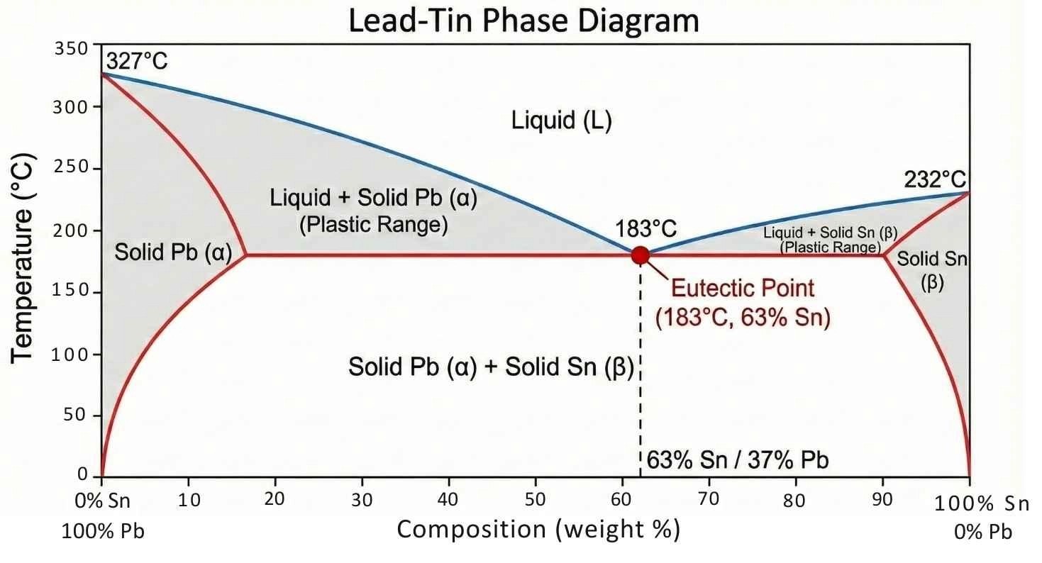
Solder Melting Point Physics: Solidus, Liquidus, and Eutectic Alloys
In order to get a grip on solder melting points, it is important to identify first that the greater part of solders are not simple elements but alloys — blended metals like Tin (Sn), Lead (Pb), Silver (Ag), and Copper (Cu). Thus, the melting process of these mixtures is usually not instantaneous.
Solidus vs. Liquidus Temperature Ranges
Engineers focus on three specific states when analyzing solder alloys:
Solidus: The highest temperature at which the alloy is completely solid. Below this point, the solder has structural integrity.
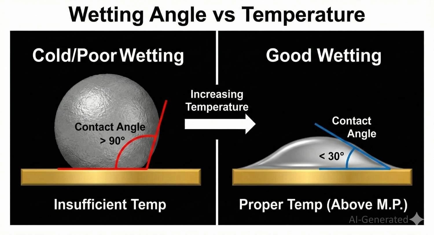
Liquidus: The lowest temperature at which the alloy is completely liquid. Above this point, the solder flows freely and can "wet" the copper pads.
The Plastic Range: For many non-eutectic alloys, there exists a "mushy" zone between the solidus and liquidus temperatures. In this state, the solder is semi-solid — part crystals, part liquid.
Engineering Risk
If a solder joint is mechanically disturbed while in the plastic range (e.g., a conveyor belt vibration), the resulting joint will be granular, dull, and electrically unreliable. This is known as a "disturbed joint."
What is Eutectic Solder and Why Does it Matter?
This brings us to the concept of Eutectic solder. A eutectic alloy has a specific ratio of metals that eliminates the plastic range. For a eutectic alloy, the solidus and liquidus temperatures are identical.
Example: The classic Sn63Pb37 (63% Tin, 37% Lead) is a eutectic alloy. It turns from solid to liquid instantly at exactly 183°C.
This "instant freeze" property is highly desirable in manufacturing because it minimizes the window of opportunity for defects to form during the cooling phase.
Optimizing SMT Reflow Profiles for Solder Melting Points
In a professional assembly environment such as JLCPCB PCB Assembly, knowing the melting point is just the first step. You cannot just set an oven to 217°C for SAC305 and hope for good results. The whole reflow process has to be done according to a certain thermal profile in order to activate the flux and guarantee that the soldering will be done right.
A standard reflow profile consists of four zones, heavily dictated by the alloy's properties:
Preheat Zone
The assembly is slowly heated to activate the flux and drive off volatile solvents.
Soak Zone
Temperature stabilizes just below the solder melting point. This large component (such as inductors) and small component (such as 0402 resistors) heating up together ensures that no tombstoning occurs.
Reflow Zone (TAL)
This is the critical spike. The temperature pushes past the liquidus point. Peak Temp: Usually 20°C to 40°C above the melting point (e.g., 245°C for SAC305). Time Above Liquidus (TAL): The solder must remain molten for 60–90 seconds. Too short, and the solder won't wet the pad; too long, and the heat damages the PCB or creates a brittle Intermetallic Compound (IMC) layer.
Cooling Zone
Rapid cooling to freeze the solder into a fine-grain structure.
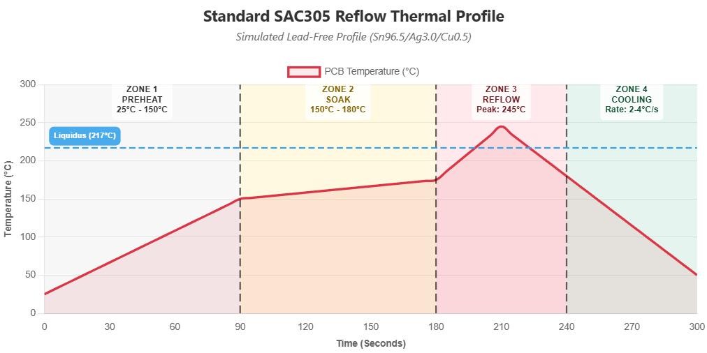
JLCPCB SMT Assembly
At JLCPCB, our SMT lines utilize advanced 10-zone reflow ovens. Our engineers customize these thermal profiles based on whether you select "Leaded" or "Lead-Free" assembly in your order, ensuring the solder melting point is reached safely without thermally shocking your sensitive components.
Critical Factors Affecting Solder Melting Point Selection
Why not just use the lowest melting point solder for everything to save energy? Several technical factors dictate the choice.
Component Thermal Sensitivity and Melting Thresholds
Some components, such as plastic OLED screens or specific electrolytic capacitors, cannot withstand the 245°C peak temperature required for SAC305. In these cases, a low-temp Tin-Bismuth solder (melting at 138°C) is necessary.
PCB Substrate Tg vs. Solder Melting Temps
The Glass Transition Temperature (Tg) of the FR-4 material is the point where the rigid PCB begins to soften and expand.
Standard FR-4 Tg: ~130°C – 140°C.
High Tg FR-4: >170°C. If your lead-free reflow process requires high heat, the PCB expands significantly in the Z-axis (thickness). If the expansion is too drastic, it can rip the copper plating inside the via holes (barrel cracks). For high-reliability lead-free assembly, JLCPCB recommends choosing High-Tg FR-4 during the quoting process.
Service Temperature and Alloy Stability
The environment where the device lives matters. An automotive sensor under the hood might see ambient temperatures of 120°C. If that sensor is soldered with Tin-Bismuth (melting at 138°C), the joints will soften and fail during operation. The service temperature should generally remain well below the alloy's solidus point.
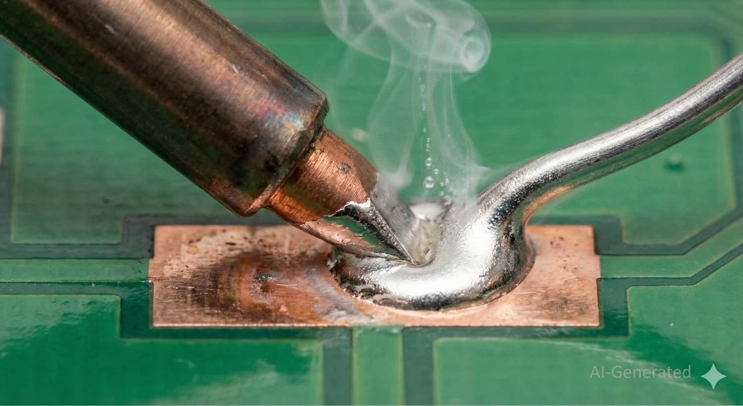
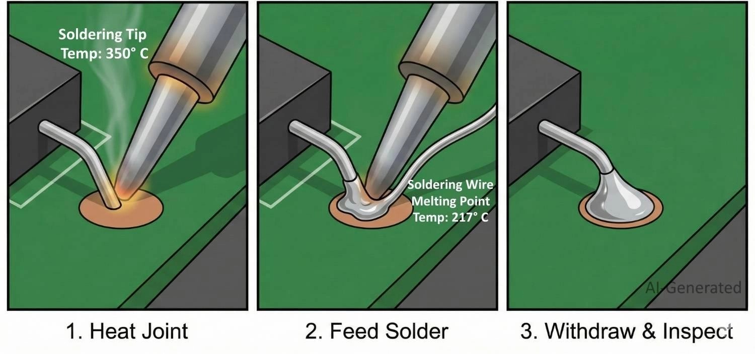
Solder Melting Point in Rework and Hand Soldering
The solder melting point also dictates how manual rework must be handled.
Iron Temperature: For hand soldering, the iron tip acts as a heat reservoir. It must be set significantly higher than the melting point to transfer heat quickly — typically 350°C for leaded and 380°C – 400°C for lead-free.
Desoldering: One popular technician method for getting rid of a hard-to-remove lead-free component is to cover the joint with leaded solder. The soldering creates a new mixed alloy that has a lower melting point; hence, the component can be taken out with less heat stress on the pad.
For complex designs where hand soldering carries a high risk of bridging or overheating, utilizing JLCPCB SMT stencils ensures precise paste application. This allows you to reflow components using a hot plate or oven, guaranteeing the entire board reaches the melting point uniformly.
FAQ about Solder Melting Points
Q: Can I mix leaded and lead-free solder during rework?
Technically, mixing leaded and lead-free solder is possible, but not recommended for high-reliability electronics. The combination of SnPb (Leaded) and SAC305 (Lead-free) results in forming a "ternary" alloy whose melting point is undefined, and it is sometimes lower than that of either original alloy (approx. 177°C). Although this promotes component removal (desoldering), it may create 'hot tearing' or phase segregation, which results in a weaker joint if it is unintentionally left on the board.
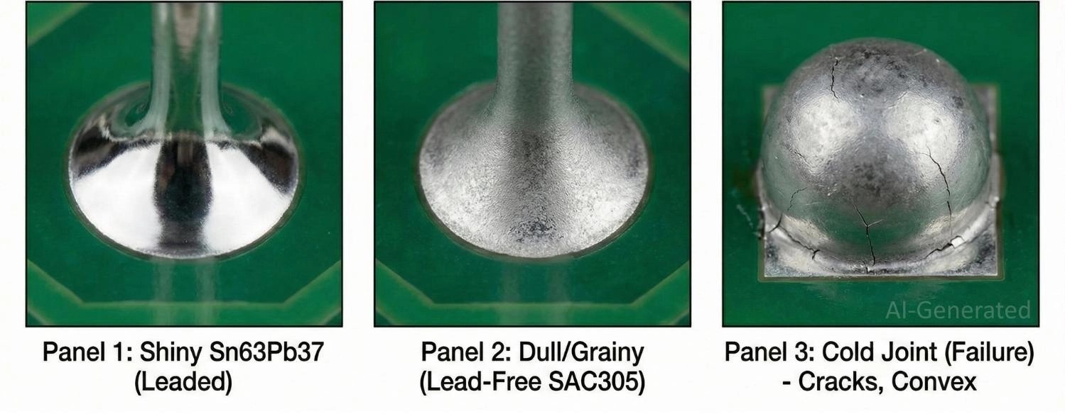
Q: Why do my lead-free solder joints look dull? Is this a "cold joint"?
Not necessarily. A classic "cold joint" (caused by not reaching the melting point) looks granular and dull. However, perfectly good SAC305 joints also look dull and grainy compared to the shiny mirror finish of Sn63Pb37. This is due to the natural grain structure of the high-tin alloy as it cools. Visual inspection criteria must be adjusted when switching from leaded to lead-free processes.
Q: How does "Thermal Mass" affect the melting point in the oven?
The melting point of the solder is fixed, but the time it takes for a specific pad to reach that temperature varies. A small resistor pad might reach 217°C in 3 minutes, while a USB connector ground pin connected to a large copper plane might only reach 200°C in the same time. This is why JLCPCB engineers optimize the "Soak Zone" of the reflow profile — to allow heat to equalize across the board so that heavy copper areas hit the melting point at the same time as small pads.
Q: Does old solder paste affect the melting point?
The metal alloy itself does not change melting points as it ages, but the flux degrades. Old flux loses its ability to remove oxides. If the oxides aren't removed, the solder cannot "wet" the pad even if the oven is well above the melting point. The solder will simply ball up on top of the pad (graping effect — solder paste balling due to insufficient flux activity) rather than flowing into a joint.
Q: What happens if I reflow a board twice?
Double-sided SMT assembly requires the board to go through the oven twice. The solder joints on the first side will re-melt during the second pass (unless using glues or low-temp alloys). While the joint will reform, each reflow cycle increases the thickness of the Intermetallic Compound (IMC) layer. Too many reflow cycles can make the joint brittle and prone to fracture under physical stress.
Conclusion: Solder Melting Points in Electronics Manufacturing
Knowing the melting point of solder is a very important factor in electronics manufacturing. It is the property that bridges the gap between material science and production. No matter if you are playing with the sharp eutectic point of Sn63Pb37 or dealing with the higher thermal demands of SAC305, accuracy is of utmost importance. Just a few degrees off can result in the formation of cold solder joints, lifting of pads, or even destruction of silicon.
Make sure your next project complies with the highest industry standards. By mastering these thermal characteristics, you can adjust your product design to ease the manufacturing process.
Popular Articles
• Common PCB Assembly Methods and Soldering Techniques Explained
• What Is BGA Void? Causes, IPC Limits, and Solutions
• SMD Soldering Tools You Need: Complete Guide from Beginner to Pro
• Reflow Soldering: Everything You Need to Know
• SMT Assembly Process Explained and Equipment Used: A Step-by-Step Guide to PCBA Manufacturing
Keep Learning
Common PCB Assembly Methods and Soldering Techniques Explained
Whether you're designing your first prototype or scaling up to production, understanding PCB assembly methods and soldering techniques is crucial to achieving reliable, high-performance circuit boards. Modern PCBA primarily relies on Surface Mount Technology (SMT) and Through-Hole Technology (THT)—each offering unique advantages for component density, durability, and manufacturability. In this guide, we'll break down the major PCB assembly methods, key soldering techniques such as reflow and wave sold......
12 Professional Soldering Tips and Tricks Every Beginner Should Know
Soldering is not merely "gluing" metal; it is a metallurgical process that creates an intermetallic compound (IMC). This molecular bond ensures the electrical and mechanical integrity of your device. A poor joint might pass a quick visual check but will inevitably fail under vibration or thermal stress, leading to "ghost" bugs and hardware failures. These soldering tips and tricks focus on practical, repeatable techniques used in professional electronics soldering—from correct heat transfer and flux u......
Solder Melting Point Guide: Chart, Alloy Types, and Reflow Considerations
In the precise world of electronics manufacturing, a difference of just a few degrees can mean the distinction between a perfect, reliable solder joint and a catastrophic "cold" joint failure. While many hobbyists view soldering simply as "melting metal to stick things together," professional PCB assembly requires a nuanced understanding of thermodynamics. The solder melting point is not simply a single value listed in a datasheet; it is a decisive limit that determines the choice of components, the s......
The Ultimate Guide to Solder Flux: Everything You Should Know Before Soldering PCB
Soldering is needed to make almost all electronic devices. Adding solder alone won't make a joint that is strong, clean, and sound from a metallurgical point of view. Solder flux is a very important part of the process that comes in here. If you want to do your job better and make it more reliable, you need to know a lot about soldering flux, whether you're an engineer, a professional technician, or just a hobbyist. This article goes into a lot of detail about solder flux, including what it is, how it......
Flex PCB Assembly Guide: Process, Challenges, and Solutions
Flexible Printed Circuit Boards (Flex PCBs) are the foundational technology enabling the compact, innovative design of modern electronics. Because of their ability to bend and fold, they power devices from smart wearables to compact medical instruments where traditional rigid printed circuit boards (Rigid PCBs) can't be used. Achieving a functional electronic circuit from the raw plastic film demands special expertise, with flexible PCB assembly (FPCA) representing the crucial final step in this trans......
SMD Rework Guide: Tools, Temperatures, and Techniques That Prevent PCB Damage
From replacing a burned regulator to correcting wrong component values or removing solder bridges on fine-pitch ICs, SMD rework is an essential skill in electronics manufacturing and prototyping. It allows engineers to repair assembly defects, implement design changes, and recover valuable PCBs without the cost and delay of building new boards. In this guide, you will learn: What SMD rework is Common rework scenarios Tools and temperatures Safe removal and installation Package-specific techniques Real......