Rigid-Flex PCB Stackup : Flex PCB Design Guidelines and Material Selection
14 min
- Understanding Rigid-Flex PCB Stackup Structures
- Flexible PCB Materials Used in Rigid-Flex Stackups
- Standard Rigid-Flex PCB Stackup Configurations
- Critical Flex PCB Design Rules for Reliable Stackups
- Manufacturing Challenges in Rigid-Flex PCB Fabrication
- Selecting the Right Rigid-Flex Stackup for Your Application
- JLCPCB's Capabilities in Rigid-Flex PCB Manufacturing
- Frequently Asked Questions (FAQ)
Ever wonder why a rigid-flex PCB stackup has a much greater chance of failing at the fold than anywhere else on the rigid part? The copper, the dielectric, and the bond layers all hold up just fine until the board experiences a few thousand flex cycles or a single pass through the lead-free reflow oven. Then the transition zone cracks, delaminates, or lifts. It is this one observation that propels practically all design decisions in rigid-flex engineering.
A rigid-flex PCB is a single piece of board that is made up of rigid FR-4 and flexible polyimide sections without the need for connectors or cables. However, as soon as you join two different material families, you have the mechanical and thermal mismatch problem, which the stackup has to deal with. In this guide, we will go through the rigid-flex PCB stackup, inside out. It is targeted at engineers with rigid PCB design experience who wish to do it right the first time with rigid-flex.
Understanding Rigid-Flex PCB Stackup Structures
What a Rigid-Flex PCB Stackup Actually Consists
The very heart of every rigid-flex PCB stackup is a flex core, which is most often a polyimide laminate double-sided with copper. This is where the flex circuit is etched and the layers that are physically flexed. The build-up is a number of different material types surrounding the flex core:
- Polyimide flex core: A bendable dielectric for continuous copper traces throughout the transition.
- Coverlay (overlay): A polyimide film with adhesive, used to replace the solder mask in flex areas and to protect flex copper.
- Bondply: Adhesive-coated polyimide film for flex cores to laminate together.
- Rigid Dielectric (FR-4 or prepreg): placed only in rigid areas for stiffness and mounting of the components.
- Stiffeners: localized reinforcements under connectors or component pads on the flex that are made of FR-4 or polyimide.
Structural Differences Between Rigid PCBs and Rigid-Flex Designs
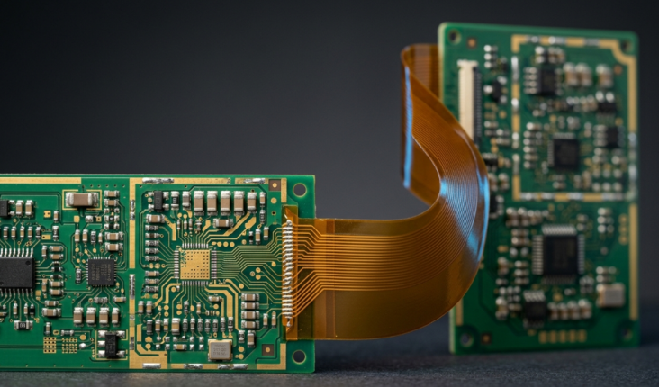
A conventional rigid board is mechanically homogeneous, with each layer having a similar coefficient of thermal expansion (CTE) and a similar modulus. A rigid-flex design is intentionally designed to combine a high modulus FR-4 area (CTE ~ 14-17 ppm/°C in-plane) with a low modulus polyimide area. This variation causes the flow of stress through the board to be different. A rigid PCB is subject to more evenly distributed stress. Rigid-flex introduces a boundary between stiff and compliant materials with a sharp concentration of stress. Another difference between the structures is the use of coverlay as opposed to liquid solder mask in flex areas.
Why Stackup Planning Determines Mechanical Reliability
The neutral bend axis location is determined by the stackup. The neutral axis is the plane that is neither in tension nor compression: copper towards the neutral axis will be subjected to a lesser amount of strain, and copper towards the outer surface of the laminate will be subjected to the greatest amount of strain. In a symmetric flex section, the neutral axis is at the geometric center. If you can balance the thicknesses of the copper and dielectric about that center, you can reduce the maximum fiber strain in the copper during the bending process. Poor stackup planning results in copper being placed away from the neutral axis, thus magnifying fatigue.
Flexible PCB Materials Used in Rigid-Flex Stackups
Polyimide vs. FR-4: Thermal and Mechanical Behavior
Polyimide is the main dielectric material used in flex layers, due to its flexibility and high thermal stability. The standard rigid dielectric is FR-4, but it is too brittle to be of any use for bending. Their behavior in a rigid-flex context is contrasted in the table below.
| Property | Polyimide (Flex) | FR-4 (Rigid) |
|---|---|---|
| Glass transition (Tg) | >250 °C | 130-180 °C |
| Continuous service temp | up to ~220 °C | ~130 °C |
| In-plane CTE (ppm/°C) | 12-20 | 14-17 |
| Z-axis CTE (ppm/°C) | ~50-60 | ~50-70 |
| Dielectric constant (Dk) | ~3.2-3.5 | ~4.2-4.7 |
| Flexibility | Excellent | None (rigid) |
Adhesive-Based vs. Adhesiveless Flex Laminates
- Adhesive-based laminate: copper foil that is joined to polyimide with an acrylic or epoxy adhesive. Lower cost and established, but the Z-axis CTE of the adhesive layer is high, and thermal endurance is lower.
- Adhesiveless laminate: Copper can be deposited or cast directly on the polyimide without any intervening adhesive. Adhesiveless laminate is generally the choice of material for multilayer rigid-flex or for any design that must endure lead-free reflow.
Overlay, Bondply, and Stiffener Material Selection
Each of the supporting flex materials has a particular function:
- Coverlay (overlay): polyimide film (usually 12.5-25 µm thick) and a thin adhesive. Seals and protects the flex copper and creates the surface for the bend area.
- Bondply is a no-flow or low-flow acrylic/epoxy adhesive on a polyimide carrier for bonding of stacked flex cores. It is important to control the resin flow here so as to prevent the resin from squeezing out into the bend areas.
- Stiffener: FR-4 or polyimide or stainless steel applied locally under connectors and component areas to stiffen where the bending is not desired.
Standard Rigid-Flex PCB Stackup Configurations
4 Layer Rigid Flex PCB Stackup Structure
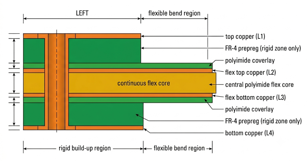
The typical starting point is the 4-layer rigid flex PCB stackup. Consists of a single double-sided flex core, which is woven continuously through the rigid areas, plus an additional rigid layer on each side of the single flex core in the rigid areas. A typical 4-layer, symmetric construction is as follows (from top to bottom):
| Layer | Material | Zone |
|---|---|---|
| L1 (top copper) | Cu on rigid prepreg | Rigid only |
| Prepreg | FR-4 prepreg | Rigid only |
| Coverlay (top) | Polyimide + adhesive | Flex + rigid |
| L2 (flex top Cu) | Copper on polyimide core | Continuous |
| Polyimide core | Flex dielectric | Continuous |
| L3 (flex bottom Cu) | Copper on polyimide core | Continuous |
| Coverlay (bottom) | Polyimide + adhesive | Flex + rigid |
| Prepreg | FR-4 prepreg | Rigid only |
| L4 (bottom copper) | Cu on rigid prepreg | Rigid only |
In this case, the flex core will be carrying L2 and L3 through the bend, and L1 and L4 will only be present within the rigid regions. Basic controlled impedance is capable with the two layers of flex copper for signals and the reference plane.
6 Layer Rigid Flex Stackup Architecture
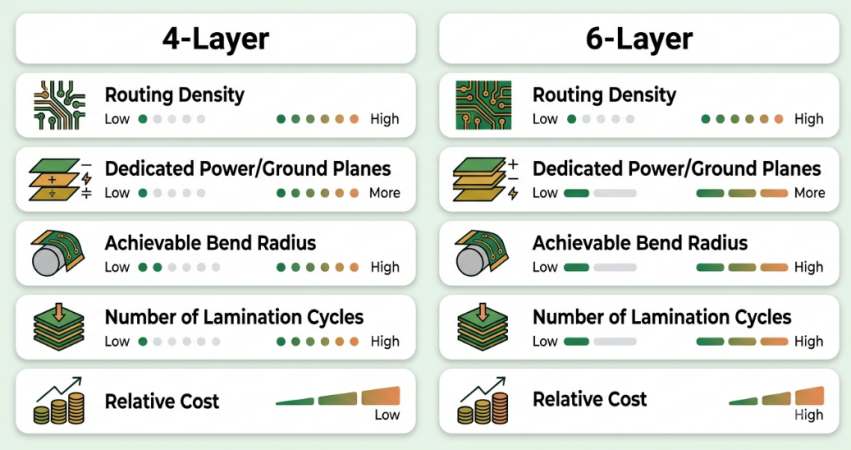
When routing channels are needed, when there is a need for dedicated power and ground planes, or if a tighter impedance control is desired, a 6-layer rigid flex stackup is used. The most effective method is to ensure that the flex section is not too thick (typically 2 layers of flex copper per 1 layer of core) and to have the additional layers in the rigid sections. In this architecture, L3 and L4 are continuous flex core, and L1, L2, L5, and L6 are constructed only in the rigid areas using prepreg and FR-4.
This is sometimes referred to as a "2-layer flex build-up with a 4-layer rigid build-up. With just 2 layers in the bend zone, the flexibility and small bend radius are retained. Additional flex cores can be added to the bend area when the application requires more conductors through the bend, but the more flex layers through the bend area, the higher the bend radius and stress will be.
Critical Flex PCB Design Rules for Reliable Stackups
Copper Cross-Hatching and Bend Area Optimization
Solid copper planes are a liability in a bend area as they are stiff and break easily. The most common solution is cross-hatching: the solid copper pours are replaced with a hatched (mesh) pattern in the flex area. Cross-hatching can help decrease bending stiffness, strain on the copper, out-gassing of the adhesive through the openings, and overall flex thickness.
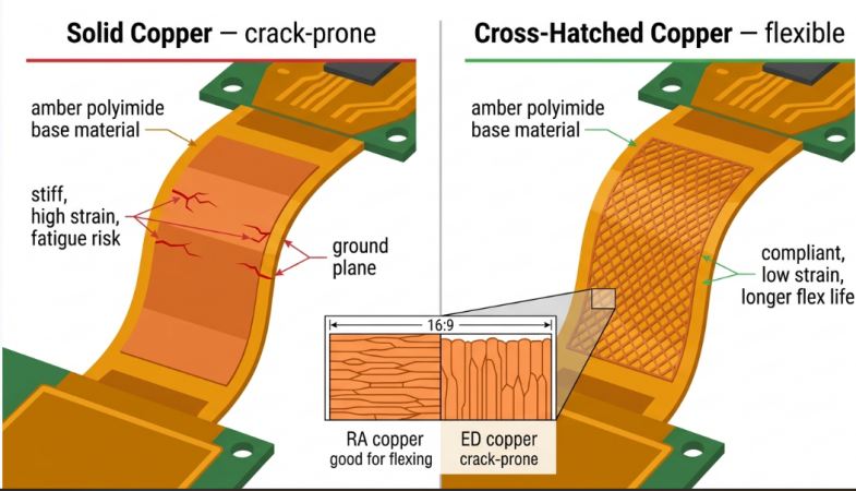
It does increase a little bit the impedance for a given geometry, thus the fill factor of the hatches should be taken care of in impedance-controlled flex routing. Use rolled-annealed (RA) copper instead of electro-deposited (ED) copper in the bend area as well. The grain structure of RA copper is elongated and is aligned in the direction of rolling, which makes it much longer lasting against flex-fatigue.
Symmetrical PCB Stackup Design to Prevent Warpage
The best defense against warpage is to use a symmetric stackup. If the distribution and thickness of the dielectrics are matched on either side of the copper centerline, the thermal stresses of lamination cancel out and do not cause bowing in the panel. This is due to the warping and cooling of the panel from the lamination temperature, as the different amounts of copper and resin on each side contract at different rates. This warpage, in turn, further reduces registration and reflow yield. Evenly distribute copper layer by layer, mirror the dielectric construction, and match the cross-hatch fill on opposite flex layers.
Via Placement Rules Near Dynamic Bend Areas
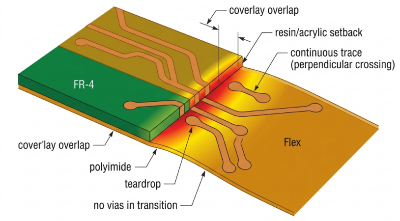
Vias are stiff, brittle, plated structures, and a bend area is the worst possible location for them. The basic rule is very simple: Ensure all vias are kept out of the bend area. When a flex bend has plated through holes or microvia, the stress is concentrated at the barrel-to-pad joint, causing the flex to crack when it is cycled. Vias should be placed in the rigid zones only and should be at least 0.5 mm (and preferably more) from the point at which the flex starts to bend. If a connection needs to cross close to the bend, then use continuous copper through the bend and over and past the bend once it reaches rigid material.
Manufacturing Challenges in Rigid-Flex PCB Fabrication
Lamination Cycles and Registration Accuracy
A multilayer rigid-flex board involves sequential lamination (flex cores are fabricated and bonded first, and then rigid build-up is added in subsequent press cycles). The high temperature and pressure of each cycle put stress on the polyimide and adhesives. The dimensional stability of polyimide is less than that of FR-4, and it can move between the layers of lamination, which makes layer-to-layer registration difficult. To compensate, more etch-factor scaling and tighter tooling are required, however, and each additional lamination cycle cumulates registration error and applies thermal stress to the adhesives.
Moisture Absorption and Reflow Delamination Risks
Polyimide is hygroscopic (has the tendency to absorb ambient moisture). Moisture can be released as steam at the high reflow temperatures of 245-260 °C and may blow apart bond interfaces, resulting in the typical "popcorn" delamination. The required countermeasure is a pre-reflow baking (typically 120 °C for a few hours) to remove absorbed moisture prior to assembly. For rigid-flex, this is a non-negotiable requirement, and, if not included, is one of the most frequent causes for field delamination.
Copper Fatigue and Dynamic Flex Failure Modes
In dynamic-flex applications, the copper is under cyclic tensile/compressive strain at the outer fibers of the bend. This starts to form microcracks over many cycles that grow until the trace opens. Failure modes fall into the following categories:
- Bend radius is too small, causing outer-fiber strain which is beyond copper's fatigue limit.
- Use of ED copper instead of the fatigue-resistant RA copper.
- Vias or stiff features inside the bend act as crack-initiation sites.
- Copper traces were drawn parallel, rather than across, the bend.
- Choosing the appropriate Rigid-Flex Stackup for the Application
Selecting the Right Rigid-Flex Stackup for Your Application
Choosing Between 4-Layer and 6-Layer Rigid-Flex Designs
For moderate routing density and impedance requirements, a 4-layer rigid-flex is the default. Being inherently thin, it can be fabricated at a lower cost, with a smaller bend radius, and is easier to fabricate. For applications requiring dedicated power and ground planes, additional routing channels, or tighter controlled impedance in the rigid areas, step up to a 6-layer rigid-flex. The trade is more expensive, requires more lamination cycles, and a smaller flex section, even though the rigid complexity increases.
Static Flex vs. Dynamic Flex Design Requirements
Static flex designs are bent once and remain stationary when a board is folded into a box. Dynamic flex designs are repeatedly flexed in service, for example, a print head or laptop hinge. The requirements are conflicting. Fully bonded stacks can be used with static flex, which is often tighter (6-10x flex thickness). Dynamic flex requires a large radius of bend (usually 20-40 times the flex thickness or greater), RA copper, single-layer-per-bend, cross-hatched planes, and often air-gap structures.
Balancing Electrical Performance, Flexibility, and Cost
Each rigid-flex stackup is a three-way compromise among electrical performance, mechanical flexibility, and costs. The more layers you purchase, the more impedance control and routing density you get, but the less flexibility and price you pay. An air gap construction provides extra life of flex, but requires more assembly. One good way to do this is to work out the non-negotiable constraint first (typically bend radius for dynamic designs, or impedance for high-speed designs), and add layers as necessary. One of the most frequent budget-busting issues of rigid-flex projects is overspecifying the number of layers.
JLCPCB's Capabilities in Rigid-Flex PCB Manufacturing
Advanced Multilayer Rigid-Flex Fabrication Processes
Now, new manufacturers like JLCPCB use controlled sequential-lamination processes with the registration accuracy required for multilayer rigid-flex. Multiple press cycles are what ensure that layer-to-layer alignment remains within spec on complex stackups, and that is through tight process control. This is critical on dense 6-layer rigid flex stackup construction, where each layer added must retain registration and the integrity of the polyimide flex core.
DFM Engineering Support for Complex Flex PCB Designs
Rigid-flex does not tolerate any sort of DFM mistakes, so design for manufacturing review cannot be neglected. JLCPCB's DFM engineering support prevents issues like too many vias in bending areas, coverlay overlap issues in the transition area, asymmetric stackup, and bend radii that are too tight to handle with the selected construction before they become scrapped panels. If you're implementing these stackup principles, the best time to identify transition-zone or symmetry issues is at the early DFM stage, when any issues are simpler to correct.

Frequently Asked Questions (FAQ)
Q: Why do rigid-flex boards delaminate during lead-free reflow?
Ans: Polyimide and flex adhesives absorb ambient moisture, and during lead-free reflow at 245-260 °C, that moisture flashes to steam and ruptures bond interfaces. A mandatory pre-reflow bake (commonly ~120 °C for several hours) drives out the moisture and prevents this popcorn-style delamination.
Q: What causes copper cracking near flex transition zones?
Ans: The transition is a stress concentration where stiff FR-4 meets compliant polyimide, so copper crossing the boundary sees the highest strain. Cracking is worsened by terminating traces at the boundary, using ED instead of RA copper, sharp corners, and insufficient coverlay overlap into the rigid region.
Q: Can vias be placed inside flexible sections?
Ans: No — vias are rigid, brittle, plated structures that crack under bending, so they must be kept out of the bend region entirely. Place vias only in the rigid zones, set back at least 0.5 mm from where the flex begins to curve.
Q: Why do rigid-flex panels warp after lamination?
Ans: Warpage comes from an asymmetric stackup, where unbalanced copper and dielectric on each side of the centerline contract unequally as the panel cools from lamination temperature. A symmetric build with balanced copper and mirrored dielectric thicknesses cancels these stresses and keeps the panel flat.
Q: What is the minimum bend radius for multilayer rigid-flex PCBs?
Ans: It depends on construction and flex type — static flex commonly allows roughly 6-10x the flex thickness, while dynamic flex typically requires 20-40x or more. Multilayer bends should be kept to as few flex layers as possible, and air-gap construction can substantially reduce the achievable radius.
Q: Are adhesiveless laminates always better for dynamic flex designs?
Ans: For dynamic flex, they are usually preferred because they are thinner, more dimensionally stable, and have lower Z-axis CTE and better PTH reliability. Adhesive-based laminates remain a valid, lower-cost choice for static designs with gentle, one-time bends.

Popular Articles
Keep Learning
Flexible Meets Durable: Understanding Rigid-Flex PCB Technology
In the rapidly evolving world of electronics, the demand for smaller, more reliable, and more versatile devices continues to grow. To meet these demands, engineers and designers are increasingly turning to Rigid-Flex PCBs. The circuit boards combine rigid and flexible substrates into a single interconnected structure. This combination allows for complex designs that can bend and flex in specific areas while maintaining rigidity in others. To manufacture rigid flex PCBs, IPC offers advice and best prac......
PCB Stiffeners: An Essential Requirement for Flexible Circuits
A printed circuit board stiffener plays an important role when it comes to offering mechanical support to a PCB. They are particularly helpful for flexible circuit boards, that given their name, are flexible and in need of stiffness in certain places. Stiffeners are particularly required when components are placed in a flex zone & the weight of these components stresses the flex material. These components provide a rigid connection from the flexible portion to the solid board. This solidity makes appl......
Choosing the Right Bend Radius for Durable Flexible PCBs
Key Takeaways Mastering the bend radius is essential for reliable flexible PCB design. Following IPC-2223 guidelines, maintain a minimum of 6× total thickness for static bends and 100× for dynamic applications, while using thinner RA copper, adhesiveless polyimide, staggered traces, and cross-hatched patterns in flex zones. Proper material selection, layer stackup optimization, and adequate clearance from stiffeners can dramatically extend flex life and prevent premature trace cracking or delamination......
Flex PCB Cost: Complete Pricing Guide & Ways to Reduce Costs
Flex PCB cost is the number that stops most projects cold. You finish a clean polyimide design, upload the Gerbers, and the quote comes back at several times higher than what the same circuit would cost on FR4. Knowing which line items drive that number is what lets you bring it down. In this guide, you will learn: Real flex PCB price ranges for prototypes and production The factors that move an FPC quote the most How does the layer count and quantity change per-board price Why flex costs more than ri......
Flexible Circuit Connector: Types, Features & Selection Guide
A flexible circuit connector clamps onto the bare copper at the end of a flex circuit, so nothing is soldered at that joint. The tail slides into the housing, and an actuator presses a row of spring contacts onto the pads. Every connector is built around one tail thickness. TE's 0.5 mm pitch 2328702 family expects 0.30 mm (12 mil) of flex, because the contact beams are deflected by exactly that dimension. Figure 1: Cross-section of a 0.5 mm pitch FPC connector with the tail inserted Feed it a bare sin......
Polyimide Flex PCB: A Complete Guide for Engineers
A polyimide flex PCB can be folded about 285,000 times when the base film is 25 µm (1 mil) thick. Make that film 75 µm (3 mil), and the same MIT fold test gives up near 6,000 cycles. Bending is a strain problem, not a material problem. Copper sits above the center of the stack, so a bend forces it to stretch around the longer outer path. Figure 1: A polyimide flex circuit folded tight, with a stiffener holding the connector A thicker stack places the copper farther out, resulting in more stretch at th......