Building Reliable High-Speed Performance with Effective Timing Analysis
14 min
- Why Timing Analysis Is Essential in High-Speed PCB Design
- Key Concepts and Parameters in Timing Analysis
- Practical Methods and Tools for Effective Timing Analysis
- Design Techniques to Optimize Timing Performance
- Manufacturing Considerations for Timing-Critical PCBs
- JLCPCB's Expertise in Timing-Critical PCB Production
- FAQ about Timing Analysis
- Conclusion
Key Takeaways
- Timing analysis is essential for high-speed PCBs — clean signals can still fail if they miss setup or hold windows.
- Focus on setup time, hold time, clock skew, and propagation delay to ensure reliable data sampling.
- Prioritize length matching, controlled impedance, and proper stackup to maintain positive timing margins.
- Combine static timing analysis with dynamic simulation for best results.
- Precision manufacturing is critical — small variations in impedance or dielectric thickness can destroy your margins.
Frankly, any board that 'looks right' in the schematic can still fail, especially when interfaces hit a few hundred Mbps. I had a DDR interface before that worked OK on 3 of 5 prototypes, and on the remaining ones, reported arbitrary read errors. The design was accepted by DRC, the impedance data were where they should be, but the data were not coming in on time. It was not a problem of signal; it was a problem of timing. I learned from that experience to consider timing analysis as a first-class citizen of high-speed design, rather than something that you bolt on at the end. If the flip-flop samples its data a few dozen picoseconds too early or too late, then cleaning the edges won't save you.
Though the signal may be beautiful, it may be incorrect, and that is simply because it appeared outside the window that the receiver was looking at. In this guide, I'd like to show you how I do timing analysis on real boards. We will discuss the importance of a high-speed PCB design, the key timing parameters such as setup time, hold time, clock skew, and propagation delay, the difference between static and dynamic methods, and the routing and manufacturing design decisions that will help you preserve timing margins. At the end of the course, you should be confident in analyzing fast interfaces in the time domain.
Why Timing Analysis Is Essential in High-Speed PCB Design
When operating at low speeds, timing is not so critical since there is ample time for a signal to stabilize before it is sampled. The clock period gets smaller and smaller as you make it run faster and faster, and those delays that you used to ignore, trace flight time, driver delay, and receiver requirements, become a significant part of the clock period. Suddenly, every picosecond counts. Timing Analysis is the field of tracking all those delays and assuring the data is meaningful at the precise moment the receiver latches it. Don't, and you're hoping for random delays to work in your favor. That's a bad bet on a fast bus, a respin.
Understanding Timing Analysis and Its Core Purpose
Timing analysis is the task of ensuring that all signals in a synchronous system arrive within the timing window for proper sampling. For a clocked design, the data driven onto one clock edge should be stable and settled before the next clock edge that is capturing the data, and it can be verified throughout the path with a timing analysis.
The main function is quite straightforward: ensure the setup and hold conditions are satisfied for each register, under all reasonable conditions. When you get it right, the system runs fine, but when you get it wrong, you get sporadic board-to-board failures that depend upon the temperature and are a pain to diagnose. Imagine that you are throwing balls at a regular pace and trying to catch them. The ball must be in hands prior to closing hands (setup) and remains in hands for a count following (hold).
The Growing Challenges in Modern High-Speed Systems
With modern interfaces, budgets for timing have been pushed to the limits. In the gigabit era, the whole bit period is reduced to a few hundred picoseconds, and there is not much margin for error in delay mismatch. This is more difficult each generation because of several factors:
- Reducing clock periods with limited allowances for skew and jitter
- Lower supply voltages are used both to reduce noise immunity and to change switching thresholds.
- Long, long, and dense routing, where small length differences become big delays.
- Source synchronous and parallel buses, such as DDR, require the matching of the byte-lane.
- Process, voltage, and temperature (PVT) variation that moves delays around in production
Key Concepts and Parameters in Timing Analysis
In order to budget a path, you must first have a solid understanding of the few parameters that define paths. All these appear in every datasheet and in all timing reports, and it is wise to know what each one represents physically. After these clicks, the timing closure math almost becomes intuitive and is simply bookkeeping of delaying versus the clock period available.
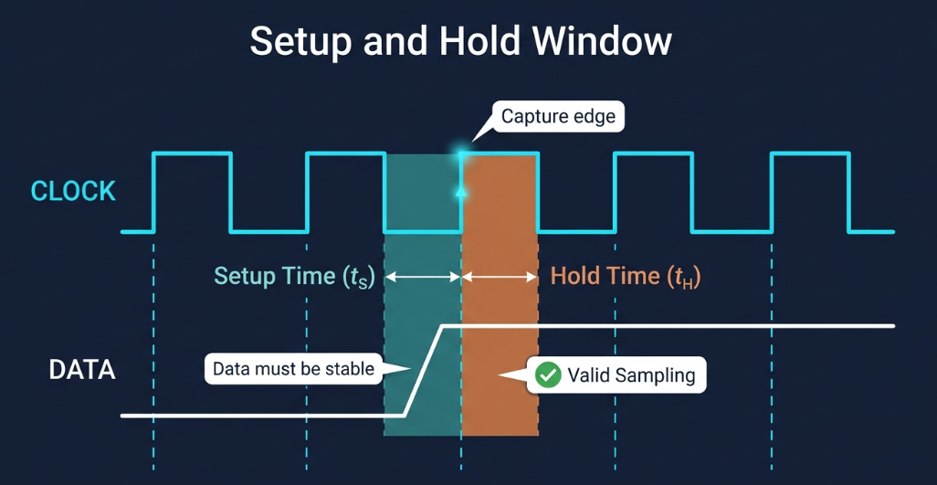
Setup Time, Hold Time, Clock Skew, and Propagation Delay
- Setup time (Tsetup) is the interval before the capturing clock edge during which the data input must already be stable. Hold time (Thold) is the interval after that edge during which the data must remain stable. Violate either, and the receiver may latch a wrong or metastable value.
- Clock-to-output delay (Tco) is how long after the launching clock edge the source register actually drives valid data. Propagation delay (Tprop), often called flight time, is the time the signal needs to travel down the trace to the receiver. On standard FR4 microstrip, propagation delay runs roughly 150 to 180 ps per inch, depending on the effective dielectric constant (Dk); stripline on the same material is a touch slower because more of the field lives in the laminate. Lower-Dk materials propagate faster, which is one reason they matter at high speed.
- Clock skew (Tskew) is the difference in arrival times of the same clock edge at two different registers resulting from primarily unequal clock-trace lengths. Depends on the sign of the skew whether it helps or hurts
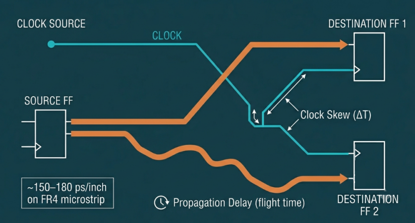
Timing Margins and Their Impact on Signal Integrity
The entire idea of analysis is to validate positive timing margins, which are also known as slack. All necessary delays are considered, and the spare time is added to that remaining. Positive slack is data that is very well within the setup and hold times; negative slack is a violation and probably a failure.
For a basic synchronous path, the setup relationship is:
Tclk ≥ Tco + Tprop + Tsetup − Tskew
The clock period needs to be sufficient to account for the output delay of the source, the flight time down the trace, and the receiver setup requirement, and factor in any clock skew between the launch and capture clocks. The difference between the leftover and the Tclk is your setup margin, Tslack = Tclk − (Tco + Tprop + Tsetup − Tskew).
There is a check for hold, which does not depend on the clock period. This is because it depends on the fastest possible path for the data, and on the clock skew, so routes that are too short or have bad skew can cause hold failures even on slow clocks. Margins are directly related to signal integrity: jitter, reflections, and crosstalk all consume margin, and a clean, controlled-impedance channel is what allows your calculated margin to exist in the real world.
Practical Methods and Tools for Effective Timing Analysis
Static Timing Analysis vs Dynamic Simulation Approaches
Static timing analysis (STA) is a mathematical analysis of all the timing paths that doesn't involve the use of real stimulus. It walks the design, calculates delay on each path, and compares it against the setup and hold requirements quickly, completely, and optimistically to find all the violating paths simultaneously. STA is corner-based: it measures the worst-case PVT combinations, and you can be certain that your design is valid throughout the entire PVT space.
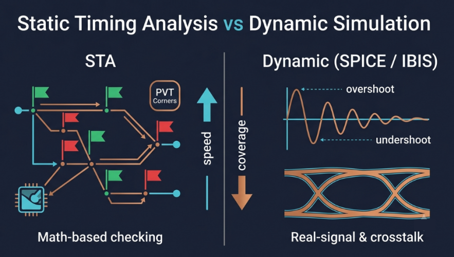
Dynamic simulation works in the other sense. It actually sends signals through models and generates actual waveforms that do reflect things that STA approximates (reflections, crosstalk, ringing, and the true shape of the switching edge). The normal tools here are SPICE for transistor-level accuracy, and IBIS models, which vendors provide to specify driver and receiver behavior without revealing their internal design.
| Aspect | Static Timing Analysis (STA) | Dynamic Simulation (SPICE/IBIS) |
|---|---|---|
| Method | Math on all paths, no stimulus | Waveform simulation with stimulus |
| Coverage | Exhaustive, every path | Selected nets and scenarios |
| Speed | Very fast | Slower, compute-heavy |
| Captures SI effects | Approximated via models | Reflections, crosstalk, ringing |
| Best for | Full-chip/bus timing closure | Critical-net verification |
Design Techniques to Optimize Timing Performance
Routing Strategies, Clock Distribution, and Termination Techniques
The largest single lever is length matching. Equalizing trace length in a parallel bus or a differential pair equalizes the flight time, directly reducing skew. If a trace is to be extended out to be the same length as the neighboring traces, the addition of serpentine (accordion) routing can be used, which increases delay without changing the impedance of the trace, as long as the gap between the meanders remains sufficiently large to prevent self-coupling. The clock is the one thing that should be treated with special care since skew on the clock infects all paths it traverses. Useful habits:
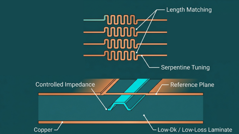
- Route clocks as matched-length, point-to-point, and balanced-tree topologies to reduce skew.
- Avoid noisy or fast switching nets that have an influence on clock traces to minimize jitter.
- Match lengths of all members in a source-synchronous group (clock and its data lanes).
- Tracing to a continuous, unbroken return plane with reference to high-speed traces.
Termination prevents reflections that would otherwise blur the edge and rob the margin. There are different topologies for series termination at the driver or parallel or Thevenin termination at the receiver, but the objective is always to match the line and ensure that the edge is clean and on time.
Layer Stackup and Material Choices for Better Timing
Your layer stackup is the electrical environment that all signals exist in. Adjacent reference planes provide a low-inductance return path for the signals, controlled spacing provides the impedance, and routing high-speed nets on stripline layers places high-speed nets in between planes to provide quieter and more predictable propagation.
Delay and loss are directly dependent on the choice of material. The dielectric constant sets propagation speed – the lower the Dk, the faster the flight time and the less delay to budget – and the loss tangent (Df) determines the amount of high frequency energy that is lost along the trace. For many designs, standard FR4 is adequate; however, for multi-gigabit links, engineers switch to low-loss, low-Dk laminates to ensure sharp edges and predictable delays over distance. The selection of the proper laminate is as much a timing decision as it is a loss decision.
Manufacturing Considerations for Timing-Critical PCBs
Impedance Control, Trace Length Matching, and Process Stability
The basis is controlled impedance, as impedance discontinuities result in reflections that affect edges and margin erosion. Maintaining the designed value of Z0 requires careful control of trace width, dielectric thickness, and copper weight, with any variation in these causing a change in Z0 and the effective delay. The geometry that forms your match to your trace length needs to be able to withstand etching as well. A mismatch in etch tolerance may cause traces to widen or narrow by varying amounts, which can result in a mismatch in the length of the traces and thus their impedances and effective delay times. The key to keeping the as-built board the same timing as the as-designed is process stability (etching, lamination, and registration panel to panel).
Quality Assurance to Maintain Designed Timing in Production
Reliable timing in volume rests on disciplined verification, not hope. The controls that matter most:
- Impedance coupons are measured on each panel to ensure controlled-impedance targets are met with a TDR.
- Lamination and prepreg management to control the thickness of the dielectric to maintain flight time on specification.
- Etch / Copper weight verification to ensure that the geometric trace is within tolerances.
- Registration accuracy for not disturbing the stripline reference spacing layer-to-layer.
JLCPCB's Expertise in Timing-Critical PCB Production
Advanced DFM Review Focused on High-Speed Timing Requirements
Things that quietly destroy timing, such as bad reference planes, unattainable length matching, and stackups that move signals too far away from the return path. Impedance specifications that can't be met by the user-selected geometry are all revealed by JLCPCB's design-for-manufacturing (DFM) review. These can be caught before fabrication, which saves a respin and safeguards the margins that you've built. Their real-time quoting and quick engineering feedback allow you to make timely decisions from the start and avoid the possibility of an expensive and failed prototype.
Precision Fabrication Ensuring Consistent Performance
In order to meet the timing analysis, the fab needs to control trace width, dielectric height, and copper weight very tightly. JLCPCB offers a wide selection of copper weights, controlled propagation delay, and controlled impedance with defined stack up, as well as consistent lamination, all of which are key aspects of controlled-impedance manufacturing that help keep propagation delay and impedance on track across a panel. Multilayer builds and stripline routing options are available, and you can select a variety of materials, such as low-loss laminates, to position high-speed signals where your timing strategy requires them.
FAQ about Timing Analysis
Q: What is timing analysis in PCB design?
Timing analysis is the process of verifying that every signal in a synchronous system arrives stably within the setup and hold window required for correct sampling. It accounts for delays like clock-to-output, propagation delay, and clock skew to prove the design clocks reliably.
Q: What is the difference between setup time and hold time?
Setup time is how long data must be stable before the capturing clock edge, while hold time is how long it must stay stable after that edge. Violating either can cause the receiver to latch a wrong or metastable value.
Q: How do I calculate timing margin?
Timing margin, or slack, is the spare time left after all delays are accounted for: Tslack = Tclk − (Tco + Tprop + Tsetup − Tskew). Positive slack means setup is met; negative slack means a violation and likely failure.
Q: What is the difference between static timing analysis and dynamic simulation?
Static timing analysis (STA) checks every timing path mathematically across PVT corners without stimulus, making it fast and exhaustive. Dynamic simulation uses SPICE or IBIS models to produce real waveforms that capture reflections, crosstalk, and edge shape on critical nets.
Conclusion
One of those topics is timing analysis, which seems abstract until you see some boards booting on some units and not others, and you discover that the data was simply arriving out of the timing window that the receiver was viewing. The entire problem becomes tractable once you begin to think of thinking in setup, hold, skew, and slack. Plan your path with Tclk ≥ Tco + Tprop + Tsetup - Tskew; length match, impedance control, static analysis, and dynamic simulation.
The thing they missed is that all of this is based on trustworthy production. If the impedance or dielectric height varies from the design value during fabrication, then a design that is close to a few picoseconds of margin is worth nothing. Combined with a disciplined timing design, a precision manufacturer like JLCPCB is how you get a board that clocks reliably, from your first prototype through volume production.
Keep Learning
PCB Basics: 50ohm PCB Trace with simple PI matching
When working with the RF (Radio Frequency) design, the transmission of signals between antennas and RF components on a PCB demands careful attention to detail. One critical aspect is the design of the antenna trace, which serves as the conduit for RF signals to propagate efficiently. In this article, we will delve into the significance of maintaining a 50 Ohm characteristic impedance for antenna traces in PCB design, along with best practices for achieving optimal performance in RF applications. Impor......
The Benefits of Coplanar Waveguide in High-Frequency PCB Design
Key Takeaways Coplanar waveguide (especially GCPW) improves high-frequency PCB performance by keeping the return path close and confining fields, which boosts signal integrity and reduces EMI/radiation. It also gives more impedance/layout flexibility (tuning both trace width and gap), but demands tighter manufacturing control of gap tolerances, copper roughness, and material Dk/Df—so field-solver impedance design and DFM checks are essential, with low-loss laminates preferred at higher GHz. Have you e......
6-Layer PCB Stackup and Buildup Guidelines
Printed Circuit Boards (PCBs) are the backbone of modern electronics, providing the necessary infrastructure for connecting and supporting various electronic components. As electronic devices become more complex and compact, the demand for multi-layer PCBs has increased. Among these, the 6-layer PCB is a popular choice for many applications. This article will delve into the specifics of 6-layer PCB stackup, its applications, optimal configurations, and guidelines for selecting the best manufacturer. W......
PCB Antenna Design: Types, Principles, and Best Practices
In the world surrounded with wireless communication, the demand for compact, inexpensive and reliable antennas has never been higher. Antennas are the application of electromagnetic waves. There are many theories and practicals available on antennas, but only few of them get recognised. For wireless data transfer the one solution can be usage of Printed Circuit Board (PCB) antennas. Using PCB antennas represents a convenient solution for integrating them directly into electronic devices, eliminating t......
Designing Antennas on PCB: A Beginner to Advance Guide
In today’s world of widespread wireless connectivity, the demand for small, affordable, and reliable antennas is higher than ever. Antennas act as real-world implementations of electromagnetic wave principles. They enable the sending and receiving of signals for a variety of wireless uses. While there is a lot of theoretical and experimental research in this area, only a few designs become widely used in actual products. Among the different options, Printed Circuit Board (PCB) antennas have become a p......
Backplane Basics: What it is and Why it Matters in High-Speed Electronics
Key Takeaways System Backbone: Backplanes act as passive interconnect boards, routing high-speed data and power across sub-cards without hosting central CPUs. Solderless Press-Fit: They use press-fit connectors to reliably hold thousands of pins while preventing thermal distortion on thick boards. Thick Multilayer Design: Built with 2.0–3.2 mm board thickness, 6–32 layers, and strict ±0.05 mm PTH hole tolerances for superior rigidity. Backdrilling for SI: Controlled-depth backdrilling removes unused v......