PCB Via Filling and Covering: Types, Methods & Applications
13 min
- What Are Vias in PCB? Understanding Via Covering & Filling
- 5 Common PCB Via Covering and Filling Methods
- Tented vs Plugged vs Untented Vias: Choosing the Right PCB Via Fill
- How to Choose the Right PCB Via Covering Method
- Design Guidelines for PCB Via Filling and Covering
- JLCPCB Via Filling and Covering Options
- FAQs about PCB Via Filling and Covering
Key Takeaways
- PCB via covering and filling are five distinct treatments—untented, tented, plugged, epoxy-filled, and copper-filled—each with different cost, reliability, and thermal trade-offs.
- Tenting is the default and lowest cost, but can show via yellowing; plugging fills the hole to prevent solder wicking and yellowing.
- Epoxy-filled and copper-filled vias enable via-in-pad with a flat, capped surface for BGA fanout and HDI designs; copper filling adds high thermal conductivity for power devices.
- Follow the decision tree based on via-in-pad need, thermal requirements, solder-ball tolerance, and probe access to pick the right method.
Every PCB has vias, but not every via is treated the same way after drilling. The choice of PCB via covering and PCB via fill — whether a via is left exposed, covered with solder mask, filled with ink, or plugged with epoxy and copper — directly affects assembly yield, long-term reliability, and manufacturing cost. This guide breaks down five common PCB via covering and filling options, explains how they differ, and helps you choose the right approach for your design.
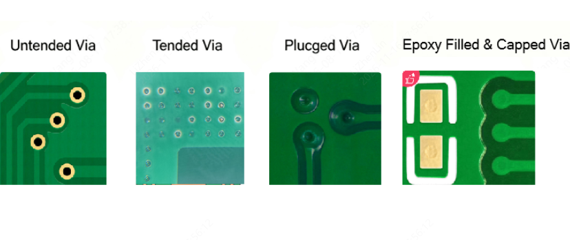
What Are Vias in PCB? Understanding Via Covering & Filling
PCB via covering (also called via protection or via finishing) refers to how the drilled and plated through-hole is treated after the outer-layer etching and solder mask stages. A via starts as a hollow copper-plated hole connecting two or more layers. Depending on the application, manufacturers may:
- Leave the via pad exposed and tinned (untented)
- Cover the via pad with solder mask while leaving the hole hollow (tented)
- Fill the hole with solder mask ink and cover the pad (plugged)
- Fill the hole with epoxy resin, cap it with copper, and cover or expose the pad (epoxy-filled)
- Fill the hole with conductive copper paste, cap it with copper, and cover or expose the pad (copper-filled)
These methods are formally categorized in IPC-4761, the "Design Guide for Protection of Printed Board Via Structures." Understanding each type is essential for hardware engineers and PCB designers who need to balance signal integrity, thermal performance, assembly requirements, and budget.
5 Common PCB Via Covering and Filling Methods
Untented Vias (Exposed / Via Opening)
An untented via has its annular ring (copper pad) left exposed — no solder mask is applied over the via pad. The exposed copper is then finished with HASL (solder), ENIG, OSP, or another surface finish. The hole itself remains hollow and open on both sides.
Advantages
- Good thermal dissipation — exposed copper conducts heat away from the board
- Accessible for test probes during ICT and flying probe testing
- Can be used as temporary test points or grounding points
- No additional process cost
Disadvantages
- Solder can wick into the hole during wave or reflow soldering, potentially leaving solder balls inside
- Exposed copper is vulnerable to oxidation and corrosion in harsh environments
- Risk of short circuits if via pads are placed too close to component pads (recommended pad-to-pad spacing ≥ 0.2 mm; use ENIG instead of HASL below this threshold)
- Not suitable for vias near fine-pitch components
Best for: Thermal vias, test point vias, and boards where probe access is required.
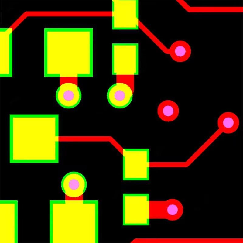
Gerber File Note: As shown in the Gerber files above, some vias have solder mask openings while others are covered by solder mask. If you submit Gerber files for fabrication, the PCB will be manufactured according to the via openings and solder mask coverage specified in those files. Always check the solder mask layers to ensure the files reflect your intended design.
Tented Vias (Solder Mask Covered)
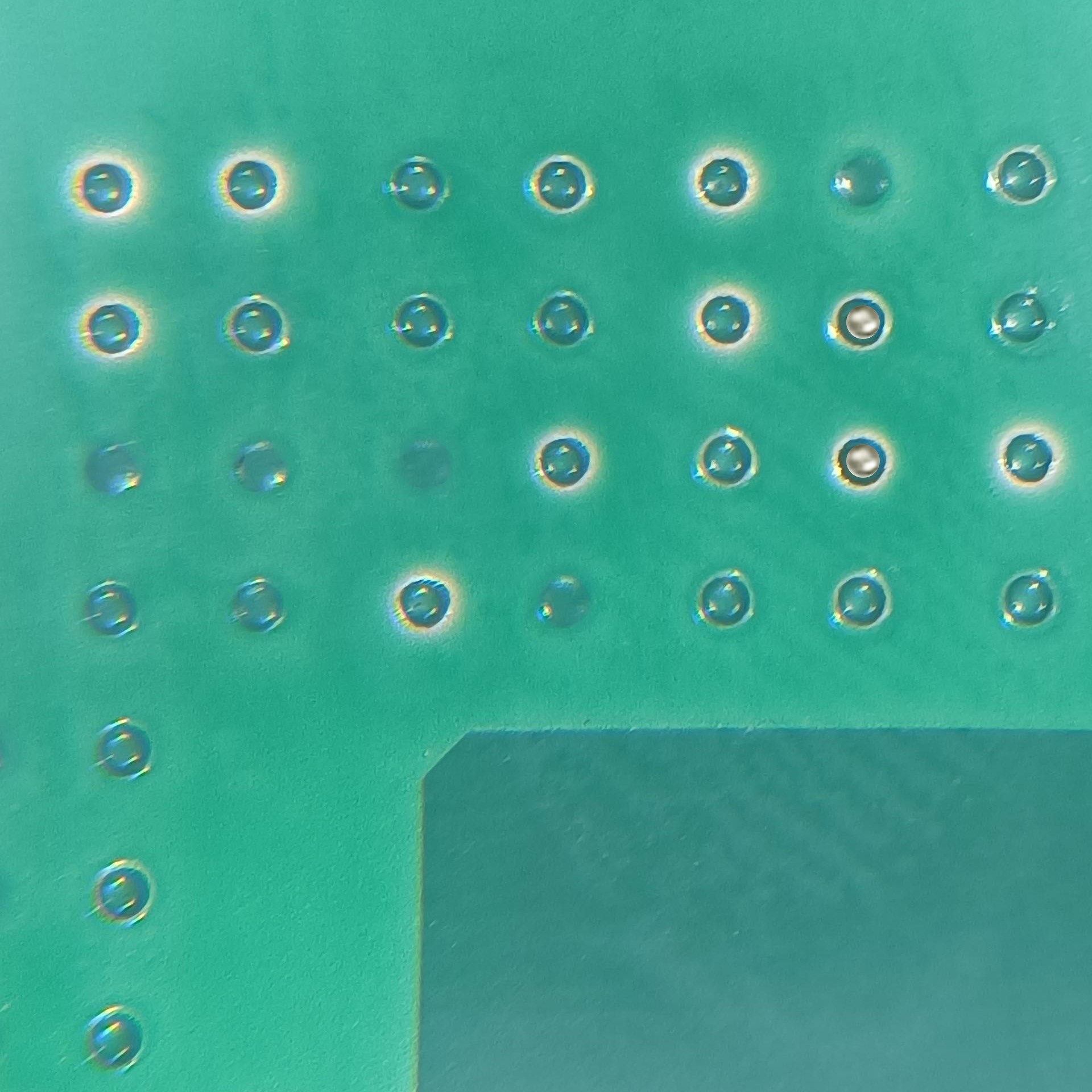
Via tenting is the most common and cost-effective via covering method. Solder mask (LPI ink) is applied over the via pad, covering the annular ring and partially bridging the hole. The hole interior remains hollow — only the surface is covered. This is the default treatment for most signal vias on standard PCBs.
Advantages
- Lowest cost — no additional process steps beyond standard solder mask application
- Prevents solder from adhering to the via pad during assembly
- Reduces risk of accidental short circuits between vias and adjacent pads
- Provides basic protection against dust, moisture, and handling contamination
Disadvantages
- Via yellowing / mask bleed: Solder mask ink is a viscous liquid. When printed over a raised via pad with a hollow center, heat curing causes the ink to flow downward into the hole, thinning the mask at the pad edge and exposing copper (yellowish-brown discoloration). This is an inherent characteristic of tenting, not a defect.
- Not a hermetic seal — the hole remains open internally
- Vias larger than 0.5 mm cannot be reliably tented; recommended via size is ≤ 0.4 mm (maximum 0.5 mm)
- Moisture or trapped volatiles can cause blistering or delamination of the solder mask during reflow
- Cannot be used for vias-in-pad
Best for: General-purpose signal vias on cost-sensitive consumer and industrial boards where via-in-pad is not needed.
Plugged Vias (Solder Mask Filled)
Via plugging (also called via filling with solder mask, a basic form of PCB via filling) goes a step further than tenting. Before the final solder mask coat, the via hole is forcibly filled with solder mask ink using an aluminum sheet or vacuum plugging process. The via is then covered with solder mask on the surface. Fill rate reaches ≥ 98%, with light opacity ≥ 95%.
Advantages
- Eliminates solder wicking into the hole — no solder balls during assembly
- Solves the via yellowing problem because the hole is filled and ink cannot flow inward
- Better protection against moisture and contamination compared to tenting
- Lower cost than epoxy or copper filling
Disadvantages
- Possible outgassing or ink bleeding (mask oil on pad surface) if not fully cured
- Surface may not be perfectly flat — not suitable for via-in-pad
- Double-sided untented vias cannot be plugged
- Single-sided untented vias with diameter < 0.4 mm can only be half-plugged (may allow light transmission)
- Vias partially on exposed pads can only be half-plugged
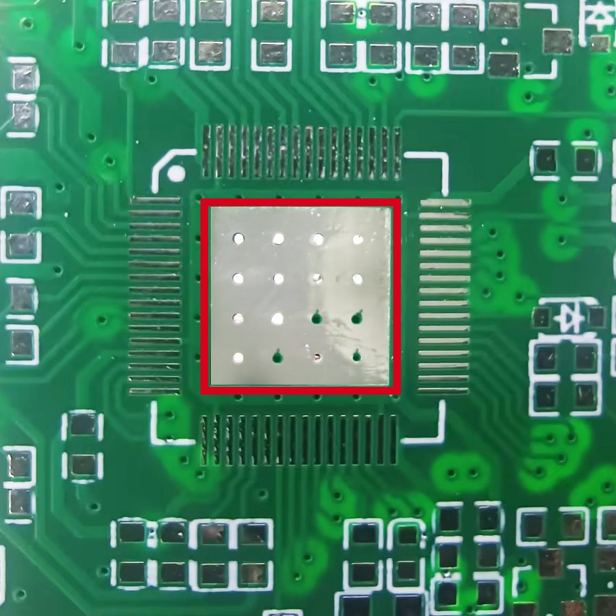
Single-sided solder mask openings may result in incomplete plugging. Solder mask ink may bleed out through the open side, and the via may remain partially unfilled, allowing light to pass through and potentially allowing solder to enter the hole during assembly. If a more reliable fill and copper cap are required, choose epoxy resin via filling with copper capping.
Best for: SMT boards where vias are near pads but not inside them; designs requiring better sealing than tenting without the cost of epoxy filling.
Epoxy-Filled Vias (Resin Plug + Capped Vias)
Epoxy via filling uses non-conductive epoxy resin to completely fill the drilled via. After curing, the surface is ground flat and then electroplated with copper (cap plating), creating a smooth, continuous copper surface. The via can then be solder-mask covered or left exposed. These capped vias are also known as via-in-pad because the capped via can be placed directly inside an SMD pad.
Advantages
- Via-in-pad capability: The via can be placed directly on an SMD pad — a game-changer for BGA and fine-pitch component fanout
- Completely flat surface — no indentation, ideal for high-density SMT assembly
- No via yellowing, no solder wicking, no outgassing
- Excellent long-term reliability — the via is fully encapsulated
Disadvantages
- Higher cost than tenting or plugging for 4-layer boards
- Via diameter must meet the manufacturer's requirements for epoxy filling; outside this range, epoxy filling is not practical
- Requires cap plating, adding process steps
- Epoxy is non-conductive and has low thermal conductivity (~0.2 W/m·K)
Quality standard: Cap plating thickness ≥ 5 μm; surface concavity ≤ 127 μm; protrusion ≤ 50 μm; fully opaque.
Best for: BGA fanout, HDI boards, high-density designs, and any application requiring via-in-pad.
Copper-Epoxy-Filled Vias (Conductive Paste + Capped Vias)
Copper-epoxy via filling follows the same process as epoxy filling, but the hole is filled with a highly thermally conductive copper paste (thermal conductivity ~8 W/m·K) instead of non-conductive epoxy. The surface is then cap-plated with copper. This method is sometimes called "thermal via-in-pad."
Advantages
- All the benefits of epoxy filling (via-in-pad, flat surface, no yellowing)
- Superior thermal conductivity: Copper paste conducts heat ~40× better than epoxy, making it ideal for power device thermal vias
- Better current-carrying capacity than epoxy-filled vias
- Fully opaque and reliable
Disadvantages
- Highest cost among all five methods
- Same diameter restriction: 0.15–0.55 mm
- Copper paste material is more expensive than epoxy
Quality standard: Same as epoxy filling — cap plating ≥ 5 μm, concavity ≤ 127 μm, protrusion ≤ 50 μm.
Best for: Power electronics, thermal via arrays under BGA packages, high-current designs, and applications requiring both via-in-pad and enhanced heat dissipation.
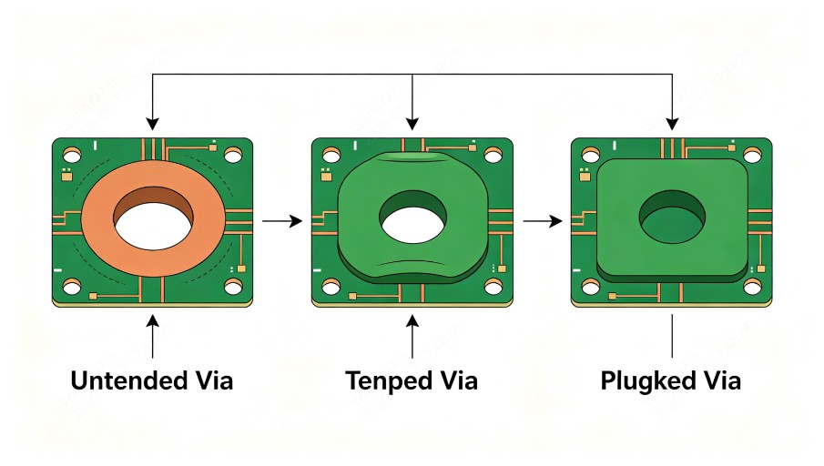
Tented vs Plugged vs Untented Vias: Choosing the Right PCB Via Fill
The three most commonly confused methods are tenting, untenting, and plugging. Here is a side-by-side breakdown:
| Feature | Untented Via | Tented Via | Plugged Via |
|---|---|---|---|
| Hole interior | Open, hollow | Open, hollow | Filled with solder mask ink |
| Pad surface | Exposed copper, tinned | Covered with solder mask | Covered with solder mask |
| Solder wicking | High risk | Low risk | None |
| Via yellowing | N/A | Common | None |
| Surface flatness | Concave (open hole) | Slightly concave | Mostly flat |
| Via-in-pad? | No | No | No |
| Relative cost | Lowest | Low | Medium |
| Thermal performance | Best (exposed copper) | Poor | Poor |
How to Choose the Right PCB Via Covering Method
Follow this decision tree to select the appropriate via covering for your design:
- Does the via need to sit inside an SMD pad (via-in-pad)? Yes → Choose epoxy filling or copper filling. No → Continue.
- Is the via primarily for heat dissipation under a power device? Yes → Choose copper filling (if via-in-pad) or untented (if not). No → Continue.
- Can you tolerate solder balls or via yellowing? No → Choose plugged vias. Yes → Continue.
- Do you need test probe access on the via? Yes → Choose untented. No → Default to tented (lowest cost).
| Design Scenario | Recommended Method | Reason |
|---|---|---|
| BGA / fine-pitch IC fanout | Epoxy-filled (via-in-pad) | Enables direct pad vias, saves routing space |
| Power device thermal via array | Copper-filled (thermal via-in-pad) | High thermal conductivity + flat surface |
| General signal vias, cost-sensitive | Tented (default) | Lowest cost, adequate protection |
| Vias near SMD pads, no via-in-pad | Plugged | Prevents solder wicking, no yellowing |
| Test points / thermal pads | Untented | Exposed copper for probing or heat dissipation |
| High-reliability / industrial | Plugged or epoxy-filled | Better sealing and long-term protection |
Design Guidelines for PCB Via Filling and Covering
- Via size: For tented vias, keep diameter ≤ 0.4 mm (max 0.5 mm). For epoxy/copper filling, use 0.15–0.55 mm.
- Annular ring: Ensure sufficient copper ring around the via for reliable tenting or plugging.
- Untented via spacing: Keep untented via pads at least 0.2 mm from adjacent component pads; use ENIG instead of HASL for tighter spacing.
- File format: Provide native PCB files (EasyEDA, Altium, KiCad) when ordering plugged or filled vias — manufacturers can auto-detect vias. With Gerber only, specify which via sizes or locations need plugging/filling in the order notes.
- Mixed methods on one board: It is common to use different covering methods on the same board — e.g., epoxy-filled vias in the BGA area, tented vias for signals, and untented vias for thermal pads. Specify clearly in the design or order notes.
- Proof check: Always review the production confirmation file (gerber review) to verify via covering is applied as intended before mass production.
JLCPCB Via Filling and Covering Options
JLCPCB supports all five via covering methods. When placing an order, you can select via covering options in the customization section. Key points:
- Tented vias are the default — no extra charge
- Untented vias require specifying "via opening" in the order notes or design files
- Plugged vias (solder mask filling) are available at additional cost; provide native files for best results
- Epoxy via filling is free for 6-layer and above boards; 4-layer boards incur an extra fee
- Copper-epoxy filling is available for thermal via applications at a premium
When providing Gerber files and requesting via plugging, include a marked-up image showing which vias to plug and note the via diameters in the order remarks.
FAQs about PCB Via Filling and Covering
Q: What is the difference between via tenting and via plugging?
Via tenting covers the via pad with solder mask but leaves the hole hollow. Via plugging fills the hole with solder mask ink before covering the pad. Plugging eliminates solder wicking and via yellowing, while tenting is lower cost but may show yellowing at the pad edge.
Q: What does via-in-pad mean?
Via-in-pad (VIP) is a design technique where a via is placed directly inside an SMD component pad. This requires epoxy or copper filling with cap plating to create a flat, solderable surface. Tented and plugged vias cannot be used for via-in-pad because their surfaces are not flat enough for reliable SMT assembly.
Q: When should I use copper-filled vias instead of epoxy-filled?
Use copper-filled vias when you need both via-in-pad capability and enhanced thermal performance. Copper paste has ~40× the thermal conductivity of epoxy, making it ideal for power device thermal vias and BGA thermal pads. For signal vias and standard BGA fanout, epoxy filling is sufficient and more cost-effective.
Q: Can I mix different via covering methods on the same PCB?
Yes. It is common practice to use epoxy-filled vias in BGA areas, tented vias for general signals, and untented vias for thermal or test points. Provide clear design files or order notes specifying which vias need which treatment.
Q: Why do tented vias sometimes turn yellow?
Via yellowing occurs because solder mask ink flows into the hollow via during heat curing, thinning the mask at the pad edge and exposing the underlying copper. This is an inherent characteristic of tenting, not a manufacturing defect. Plugged or filled vias do not have this issue because the hole is already filled.
Conclusion on PCB Via Filling and Covering
Choosing the right PCB via covering and filling method is a balance between cost, reliability, thermal performance, and assembly requirements. Tenting is the default for general signal vias, plugging prevents solder wicking and yellowing, while epoxy and copper filling enable via-in-pad for BGA fanout and high-density designs. By understanding the five IPC-4761 methods and following a simple decision tree, designers can select the treatment that best fits each via and avoid costly assembly and reliability issues downstream.
Keep Learning
Technical Guidance: Character Design Specifications
To facilitate component assembly, future maintenance, and traceability of PCB manufacturing information (such as manufacturer, production date, batch number, etc.), various character markings are typically silk-screened onto the PCB. These include component designators, polarity marks, test point labels, company logos, and production traceability information. Traditional PCB character silk-screening uses the screen printing process, hence the term “silk-screen characters.” High-definition characters a......
Via Filling Explained: Key Techniques, Benefits, and Solutions for High-Performance PCBs
Key Takeaways Via filling completely fills plated through-holes and microvias with epoxy or conductive copper paste, followed by planarization and copper capping (POFV). It eliminates voids, solder wicking, and thermal/mechanical issues while enabling reliable via-in-pad designs. Benefits include superior heat dissipation (up to 8 W/m·K), better signal integrity, higher mechanical strength, and improved assembly yields. JLCPCB provides free non-conductive filling + POFV on 6+ layer boards. Ideal for H......
How Fiducial Markers Guarantee Perfect Alignment in Professional PCB Fabrication
Today, the most sophisticated pick-and-place machine can place a 0.5 mm pitch QFP on its footprint, board after board, thousands of times, and never miss. It is not only a matter of expensive cameras or high-quality servos, but it begins with a little, very small copper dot, simply hanging there in the corner of your PCB. That dot represents a fiducial marker, and without it, even the smoothest SMT line would be laying components in the dark. The unrecognized heroes of automated assembly are the fiduc......
PCB Via Filling and Covering: Types, Methods & Applications
Key Takeaways PCB via covering and filling are five distinct treatments—untented, tented, plugged, epoxy-filled, and copper-filled—each with different cost, reliability, and thermal trade-offs. Tenting is the default and lowest cost, but can show via yellowing; plugging fills the hole to prevent solder wicking and yellowing. Epoxy-filled and copper-filled vias enable via-in-pad with a flat, capped surface for BGA fanout and HDI designs; copper filling adds high thermal conductivity for power devices. ......
Technical Guidance: Mouse Bite Panelization Guide
The conventional method of panelization uses V-grooves. However, for irregularly-shaped boards or special requirements (such as JLCPCB's economic SMT assembly), mouse bite panelization, which resembles postage stamps on an envelope, is required. PCBs panelized using this method are called "mouse bite panels" or "mouse bite connections". Mouse bite panelization can be referred to as "universal panelization." As long as there is a position to add mouse bites, boards of various shapes can be interconnect......
Technical Guidance: V-Cut Panelization Standards
For boards with regular rectangular shapes, V-cut (V-scoring) panelization is an efficient method. This process involves cutting V-shaped grooves of a specific depth on both sides of the panel along the board boundaries, leaving a thin web of material (typically about 1/3 of the board thickness) that allows easy manual separation after SMT assembly. After separation, minor thread-like fibers or rough edges may remain and can be lightly scraped off. Due to material expansion and cracking during depanel......