From Physical Board to Production: How to Master PCB Reverse Engineering
14 min
- What Is PCB Reverse Engineering and Why Does Your Project Need It?
- Step-by-Step Guide: How to Reverse Engineer a PCB Efficiently
- Overcoming Key Technical Challenges in Complex PCB Reverse Engineering
- Essential Considerations When Choosing a PCB Reverse Engineering Service
- FAQ about PCB Reverse Engineering
- Conclusion
Key Takeaways
- Stick to a 3-Stage Workflow: Process sequentially from BOM mapping to netlist extraction, and finally DFM reconstruction.
- Trust the Measured Netlist: Always verify connections directly with a meter; electrical data overrides optical scans.
- Match Imaging to Board Density: Use scans for outer layers, but rely on micro CT or delayering for blind/buried HDI vias.
- Recalculate Trace Impedance: Never copy trace widths directly—re-calculate for your target layer stackup and dielectric thickness.
- Decode ICs by Context: Identify unmarked chips by tracing power, pinouts, adjacent parts, and live signals.
Every time a PCB reverse engineering job is needed, the bad news is that the PCB still functions, the vendor is no longer in business, and the source files are missing. You are without any design information behind your physical object.
In this guide, you will learn:
- What PCB reverse engineering is, and where it is legitimate
- The three-stage workflow, from component mapping to a verified netlist
- Which imaging method to use: flatbed, X-ray, CT, or delayering
- How to map blind and buried vias on HDI boards
- How to identify unmarked and house-numbered ICs
- Why a controlled-impedance pair cannot be redrawn at the same width
- What to check before sending recovered Gerbers to a fab
What Is PCB Reverse Engineering and Why Does Your Project Need It?
PCB reverse engineering is the process of studying a finished board and rebuilding the design data used to make it. You start with copper and solder, and finish with a schematic, a bill of materials, and fabrication files.
Defining the Core Concept
Think of a four-layer board as four street maps glued face to face. You can read the top and bottom maps with your eyes. The two in the middle are sealed inside cured epoxy, and the only way to read them is to cut in or shine X-rays through. Reverse engineering recovers three separate things, and they are not the same job:
- The bill of materials (BOM). Every part, its value, its package, and a modern equivalent where the original is dead.
- The netlist. A plain list of which pin connects to which pin. This is the electrical truth of the board.
- The physical layout. Copper shapes, drill sizes, and layer order are exported back out as Gerber and drill files.
Stop after the netlist if all you need is documentation. You only need the layout if you intend to build the board again. Recover the netlist first. Everything else is a redrawing exercise once the connections are known.
Benefits of PCB Reverse Engineering for Hardware Projects
The real reader here is not a hobbyist copying a gadget. It is an engineer holding a board that a factory depends on, with no source files anywhere in the building. That situation shows up in five recurring forms:
- Repairing equipment whose vendor is gone: A packaging line or treadmill controller still runs, but the company that built the board closed a decade ago.
- Replacing obsolete parts: Zilog ended Z80 production in 2024, and microcontrollers such as the MC68HC11 vanished long before that. You cannot pick a replacement until you know what the old part did.
- Recovering your own lost documentation: Companies often lose the CAD files for boards they shipped, typically due to a tool migration or a departing contractor.
- Failure analysis: When a field return keeps burning the same driver, you need the real net topology, not a block diagram.
- Migrating a legacy design: Old boards on discontinued laminates are rebuilt using modern materials.
Reverse engineering hardware you own, for repair, maintenance, documentation, or interoperability, is routine practice and broadly protected. Selling copies of a competitor's protected design is a different act, and patents, trade secrets, and mask work rights all apply there.
Step-by-Step Guide: How to Reverse Engineer a PCB Efficiently
The PCB reverse engineering process runs in three stages, and skipping ahead is the most common way to waste a board. Each stage produces an artifact that the next stage depends on.
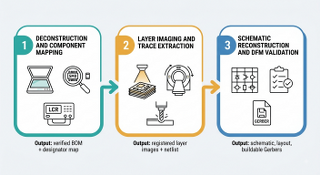
| Stage | What You Actually Do | Main Tools | What You Have At The End |
|---|---|---|---|
| 1. Deconstruction and component mapping | Photograph, catalog, desolder, and measure every part | Flatbed scanner, microscope, LCR meter, multimeter | A verified BOM and designator map |
| 2. Layer imaging and trace extraction | Expose or scan every copper layer, then align them | 2D X-ray, micro CT, abrasion, chemical strip | Registered layer images and a netlist |
| 3. Schematic reconstruction and DFM validation | Rebuild the circuit in EDA, then check it against fab limits | KiCad, Altium, EasyEDA, DFM checker | Schematic, layout, and buildable Gerbers |
Stage 1: Deconstruction and Component Mapping
Don't touch anything until you take photos of both sides of the board. Use flat lighting and a dark background, as a light background will make the drilled holes appear as copper pads. A 1200 DPI flatbed scan offers approximately 21 microns (0.8 mil) per pixel resolution, which enables reading of most 0402 markings.
Then work through the parts one at a time:
- Read and record the package markings. Two-character and three-character codes are common, so keep a decode reference for SMD transistor codes and SMD capacitor codes beside you.
- Desolder and measure anything that the marking does not settle. Ceramic capacitors carry no printed value at all.
- Record the package outline against IPC-7351 land patterns so the footprint you rebuild matches the real part.
Measure passives out of the circuit. A 0.1 uF decoupling capacitor measured in place can read several microfarads, because every other capacitor on that rail sits in parallel.
Stage 2: Layer Imaging and Trace Extraction
Outer layers are easy. Strip the solder mask or scan the bare copper, and you have your top and bottom artwork. Everything hard about this stage is the copper you cannot see. You have three ways in:
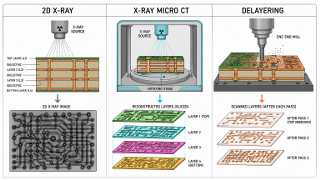
- 2D X-ray: Quick and inexpensive, and it is evident through the positions and dense copper. It "flattens" everything into a single image, meaning that a trace on layer 2 and a trace on layer 3 will overlap on the screen.
- X-ray micro CT: A rotating scan that is reconstructed into a volume from which slices can be taken. A published paper for this Zeiss Xradia 520 Versa claims voxel sizes around 14 micrometers (0.55 mil) and a field of view of 15 mm (0.6 inch), with extracted netlists that match the expected netlist exactly on the validated boards.
- Delayering: Controlled abrasion (one layer at a time – grinding or CNC milling) or chemical copper strip, scanning after each pass.
Once layer 1 is removed, it cannot be checked again, and if you have a second identical board, don't use it for checking until after the first one.
Stage 3: Schematic Reconstruction and DFM Validation
Now the recovered data becomes a design. Import the aligned layer scans into your EDA tool as background images, place the real footprints on top, and route to match. The measured netlist is the referee. If a drawn connection disagrees with the meter, the meter wins.
Rebuild the schematic in functional blocks, not in physical order. Group the power supply, then the microcontroller and its decoupling, then each interface. A schematic redrawn in physical order is technically correct and almost unreadable, which defeats the point of recovering an electrical schematic at all.
Then, validate before you order anything:
- Run a full DRC and ERC pass against your fab's real limits, not the tool defaults, using our PCB design rules guide for the clearance and annular ring numbers.
- Confirm minimum trace and space. A 1990s board often sits at 8 mil (0.20 mm), which modern rules pass easily, but a dense board may reach 4 mil (0.10 mm) or below.
- Check drill sizes and annular ring against current capability.
- Compare your netlist export against your measured netlist one final time.
Overcoming Key Technical Challenges in Complex PCB Reverse Engineering
The difficulty climbs sharply once inner layers, hidden vias, and controlled impedance enter the picture.
| Challenge | Why Ordinary Methods Fail | Method That Works | What It Costs You |
|---|---|---|---|
| Inner layers on a 4 to 8-layer board | Optical scanning sees outer copper only | Serial delayering, or micro CT slicing | CT detail drops as copper density rises |
| Blind and buried vias | 2D X-ray flattens every layer into one image | 3D CT slices, or a microsection per IPC-TM-650 | A microsection destroys that area |
| Unmarked or house-numbered ICs | There is no part number to search | Pinout probing, bench behavior, decapsulation | Custom ASICs may be unrecoverable |
| Controlled impedance nets | Copying the trace width gives the wrong impedance | Re-solve the width and gap for the new stackup | You must infer the original target |
Handling High-Density Interconnect (HDI) and Blind/Buried Vias
A through-hole via runs top to bottom, so you can see it from either face. A blind via connects an outer layer to one inner layer and stops. A buried via sits entirely inside the stack and never reaches a surface. The problem is, a buried via is invisible on both faces, and on a flat 2D X-ray, it looks identical to a plated through-hole seen from above. Micro CT solves it because slicing the reconstructed volume at each layer depth shows where a via barrel starts and stops. Laser-drilled microvias make it harder again. They run as small as 0.1 mm (4 mil) across, thinner than a human hair, and copper planes above and below absorb X-rays and darken everything behind them. HDI scans are therefore run in small tiles and stitched together.
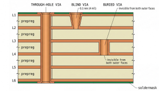
To fix this: if CT is out of budget, take a microsection through a representative via field using the manual microsectioning method in IPC-TM-650, then read the layer transitions straight off the polished cross-section under a microscope. Map the via structure before you interpret the layer images, because once you know which layer pairs connect, ambiguous traces resolve themselves.
Identifying Unmarked or Custom IC Components
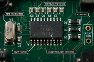
Eventually, you'll come across a chip featuring a laser-etched house number that doesn't come up in any search engine. This marking is not by the silicon vendor; it is by the OEM, and it was intentionally made unsearchable. Work it out from the outside in:
- Count pins and identify the package: A 16-pin SOIC beside a row of relay coils behaves nothing like a 48-pin QFP beside a crystal.
- Find power and ground: Probe for the pins tied to the rails, and the pinout family narrows immediately.
- Read the neighbors: A part beside a crystal and a W25Q128 SPI flash is a microcontroller. A part driving relay coils through flyback diodes is almost certainly a Darlington array such as the ULN2003.
- Scope it live: Clock frequency, logic levels, and bus protocol usually name the function even when they do not name the part.
To fix this, where the chip is a genuine custom ASIC or mask-ROM microcontroller, stop identifying and start substituting. Replacing unknown glue logic with a 74HC595 shift register, or an unknown quad amplifier with a TL074, gives you a part you can still buy in ten years.
Preserving Signal Integrity and Controlled Impedance
Here is where careful reverse engineering still produces a dead board. Trace width alone does not set impedance. Four things set it together: trace width, copper thickness, the gap down to the reference plane, and the dielectric constant between them.
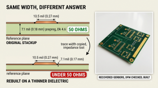
With the JLCPCB four-layer stackup, JLC7628, a single-ended 50 ohm trace on an outer layer requires approximately 10.5 mil (0.27 mm) of width on approximately 7.1 mil (0.18 mm) of prepreg of dielectric constant near 4.6. Take the same 10.5 mil trace and place it on a thinner dielectric, and it reads under 50 ohms.
Example: A motor drive board was reverse-engineered cleanly; every net matched, and every part was correct. The rebuild moved from the original six-layer board to a four-layer 1.6 mm (63 mil) stackup, and the CAN bus pair was redrawn at its original 0.20 mm (8 mil) width. On the bench, nodes dropped off the bus once the cable run passed two meters. The pair measured near 85 ohms instead of the 120 ohms CAN requires. The fix was resolving the width and gap for the new dielectric height instead of copying the old geometry.
Important: tag differential pairs during netlist extraction. Tightly coupled parallel traces of equal length running to a transceiver are the signature. Recalculate every tagged pair for the stackup you will build on, and first check how board thickness affects the stackup.
Essential Considerations When Choosing a PCB Reverse Engineering Service
Doing this in-house makes sense for a two-layer board. Beyond four layers, the imaging equipment alone rules most labs out, and a PCB reverse engineering service becomes cheaper.
Ensuring Seamless Transition from Gerber to Fabrication(JLCPCB Capabilities)
Recovered Gerbers are not the same as designed Gerbers. They carry whatever the original board did, including features a current fab may refuse, so the handoff needs a real DFM review.
Check these before ordering:
Layer count and stackup: Confirm the stackup you rebuilt on is one that the fab actually offers, because impedance depends on it.
Minimum trace and space: Standard 1 oz copper production sits around 5 mil (0.127 mm), with 3.5 mil (0.089 mm) on high-precision orders.
Via structure: Blind and buried vias need sequential lamination, which changes both cost and lead time.
Silkscreen legibility: Rebuilt silkscreen is often scaled from a scan and lands below the minimum readable height, so check it against our PCB silkscreen guide.
Design Complete? Start Manufacturing Today. JLCPCB builds 1 to 20-layer boards, holds controlled impedance to plus or minus 10 percent, offers laser-drilled microvias and blind or buried vias for HDI rebuilds, and runs an automated DFM check that flags recovered files before production.
FAQ about PCB Reverse Engineering
Q: Is PCB reverse engineering legal?
Analyzing hardware you own for repair, maintenance, documentation, or interoperability is standard practice and broadly permitted. Selling copies of a design protected by patents, trade secrets, or mask work rights is not.
Q: Can you reverse engineer a PCB without destroying it?
Yes. Use 2D X-ray for via mapping, or X-ray micro CT for full layer-by-layer reconstruction. Non-destructive imaging keeps the board testable, but detail drops as copper density and thickness rise. Delayering gives better detail and destroys the sample.
Q: How long does PCB reverse engineering take?
A simple two-layer board with marked parts takes a few days. A dense six or eight-layer board with unmarked ICs runs into weeks, because netlist verification and component identification, not imaging, eat most of the time.
Q: What do I actually receive from a PCB reverse engineering service?
It varies widely, so put it in the contract. A complete package is a BOM, a netlist, a readable schematic, correct footprints, and Gerber plus drill files. Some vendors deliver Gerber files only, which lets you rebuild the board but not modify it.
Q: What if the ICs have no readable markings?
Identify the function instead of the part. Count the pins, find power and ground, read the surrounding components, and probe the signals live. For custom ASICs or mask-ROM parts, substituting a modern equivalent is usually the only workable route.
Conclusion
PCB reverse engineering is not a trick about smart tools; it's more about the proper sequence. Recover the parts, recover the connections, and then only recover the copper. Do not trust any image or CAD export; you will know the truth from the netlist you measured with a meter.
The number of times that the final step is overlooked is the last step that the majority of teams take. A board can be completely reconstructed and fail on a new stackup – impedance, thermal behavior, and drill capability are part of the board you are building, not the one you are taking apart! Recover the design, and then re-engineer the physics to make the actual process.

Popular Articles
• The Comprehensive Guide to Circuit Symbols: Key to Understanding Electrical and Electronic Diagrams
• Design Guidelines for PCB Using FR4 Substrates
• Choosing the Best PCB Color-Enhancing Aesthetics and Functionality
• PCB Silkscreen: All You Need to Know
• PCB Board Design: A Step-by-Step Guide for Beginners
Keep Learning
How to Read and Create PCB Schematics
Key Takeaways Read Schematics: Understand symbols, net labels, and component values. Design in EasyEDA: Place components and create circuit connections. Run Design Checks: Use ERC and DRC to identify potential issues. Verify Components: Check pin assignments and PCB footprints. Prepare for Manufacturing: Validate PCB layouts and manufacturing files. Printed circuit board (PCB) design begins with a clear understanding of how the electronic circuit should function. A schematic diagram represents the cir......
Maximizing Circuit Reliability with PCB Test Points and Smart DFT
Key Takeaways Early Fault Catching: Test points drastically reduce diagnosis time and prevent costly field failures. Standard Pad Sizing: Use 1.0 mm flat copper pads with 2.54 mm spacing for optimal fixture contact. Protect High-Speed Signals: Keep branch traces short to prevent capacitive loading and resonance. Single-Sided Access: Place all test pads on the bottom layer to cut fixture costs. Right Test for Volume: Use flying probe for prototypes and bed-of-nails ICT for mass production. A PCB test p......
The Comprehensive Guide to Circuit Symbols: Key to Understanding Electrical and Electronic Diagrams
Note Need a quick reference while reading schematics? Download our free, printable Circuit Symbols Cheat Sheet (PDF), featuring the most common IEC and ANSI symbols organized by category. Keep it on your desktop or print it for easy reference at your workbench. ⬇ Download the Free Circuit Symbols Cheat Sheet (PDF) Every electronic diagram is written in a visual language, and circuit symbols are its alphabet. From your first electrical schematic to a multi-layer board, knowing circuit symbols can make ......
Design Guidelines for PCB Using FR4 Substrates
Material substrate concerns are necessary while designing electrical circuit boards. This is due to the fact that printed circuit boards cannot be manufactured without the appropriate PCB materials. When developing and producing circuit boards, the substrate material must be taken into account just as much as the copper layers, silkscreen, and surface polish. Generally speaking, non-conductive materials like porcelain, Marlon, FR4, and the like must be used for PCB substrates. Depending on its intende......
Choosing the Best PCB Color-Enhancing Aesthetics and Functionality
Key Takeaways Choosing the best PCB solder mask color involves balancing aesthetics, visibility, and functionality. Green remains the top choice for superior contrast and inspection, while black offers premium appeal, white excels in LED applications, and other colors like purple and red provide unique design options. The ideal color depends on your priorities in inspection ease, thermal performance, and brand image, with minimal impact on electrical performance when using proper silkscreen contrast. ......
4 Layer vs 6 Layer vs 8 Layer PCB: How to Choose the Right Stackup
Random selection of layers in electronics may lead to serious signal integrity issues. That's why we always design our stackup before designing the PCB. Stackup decides the type of PCB and how it gonna perform under high-frequency conditions. There are a lot of things that directly affect the stackup of the PCB, related to impedance matching, routing density, signal and power integrity, electromagnetic compatibility (EMC), and cost. Knowing the requirements before design and the most critical componen......