
Improving Heat Dissipation : The Smart Use of Thermal Pads in PCB Design
12 min
- What Thermal Pads Are and Why They Matter
- Key Benefits of Using Thermal Pads
- Design Guidelines for Effective Thermal Pad Implementation
- Manufacturing Best Practices for Thermal Pad PCBs
- JLCPCB's Expertise in Thermal Pad Solutions
- FAQ about PCB Thermal Pad
- Conclusion
Key Takeaways
Optimizing PCB thermal pad design and via arrays is essential to prevent semiconductor failures caused by FR4's low thermal conductivity. By implementing a 1.0–1.2 mm via pitch and keeping solder voiding below 25% through segmented stencils, designers can eliminate localized hot spots and boost board reliability from prototype to high-volume production.
Have you ever considered that the thermal conductivity of a normal FR4 PCB is only about 0.3 W/mK? That is an acceptable number for low-power circuits. However, as soon as you begin adding power-hungry ICs, voltage regulators, or high brightness LEDs to your board, you have an adversary to reliability, which doesn't make a sound: heat. That's where a good PCB thermal pad can come in handy.
One of the most frequent issues that leads to an early life failure of electronic assemblies is heat. For every 10°C increase in junction temperature, the life time of a semiconductor can be reduced by half. Using only copper traces and ambient air flow as a thermal management solution means you are compromising performance and lifespan. In this article, we'll delve into the nature of thermal pads, their significance, the criteria for effective design, and the manufacturing processes that guarantee their performance.
What Thermal Pads Are and Why They Matter
Definition and Basic Function of Thermal Pads in PCBs
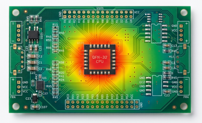
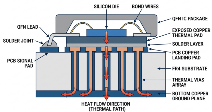
Thermal pads are large exposed copper surfaces on the underside of surface-mount component packages that are used to transfer heat directly from the die to the PCB. They are available on packages such as QFN (Quad Flat No-lead), DFN, PowerPAD, and on a lot of exposed-pad power ICs. The thermal pad is different from signal pins, which transmit electrical information, and its purpose is to serve as a heat highway.
The thermal pad conducts heat down when the component is running to a matching copper landing pad on the PCB. From there, an array of thermal vias conducts heat to internal copper planes or to the other side of the board. This allows the creation of an uninterrupted thermal path from the component junction right through the board stackup.
When Thermal Pads Become Necessary for Thermal Management
There is no need to manage thermal pads for every design. Standard copper traces and pours easily deal with the thermal load for low-power microcontrollers that draw a few milliamps. However, there are definite scenarios where thermal pads are a must. If the component dissipates more than 0.5-1 watt in a small package, it should be connected with a properly designed thermal pad. This includes:
- Power management ICs (PMICs), voltage regulators (LDOs, DC-DC converters)
- Motor driver ICs with continuous currents of more than 1A.
- High brightness LED packages with thermal slugs
- High-frequency RF power amplifiers produce large amounts of heat.
- Class AB or Class D audio amplifier ICs
- MOSFET packages such as DPAK, D2PAK, and PowerPAK
- Thermal Pads provide a number of benefits, including:
- Improved Heat Transfer from Hot Parts to PCB.
Key Benefits of Using Thermal Pads
Enhanced Heat Transfer from Hot Components to PCB
The most obvious benefit of thermal pads is that they greatly increase heat conductivity. For copper, the direct copper-to-copper solder connection has a thermal conductivity of approximately 385 W/mK, and the solder alloys have a thermal conductivity of approximately 50 W/mK. This is compared to the FR4 dielectric material, which has a thermal conductivity of 0.3 W/mK, which makes routing heat through copper, as opposed to the laminate, extremely important. Let's put some numbers in perspective. Let's take a look at a 2-watt, 5x5 mm QFN voltage regulator.
| Thermal Path | Thermal Conductivity (W/mK) | Relative Performance |
|---|---|---|
| FR4 substrate only | 0.3 | Baseline (poor) |
| Copper pad (no vias) | 385 | Excellent lateral spreading |
| Solder joint to pad | 50 | Good vertical transfer |
| Thermal vias (filled) | ~15-25 (effective) | Good vertical through-board |
| Aluminum heatsink | 205 | Excellent external dissipation |
Reduced Hot Spots and Improved Overall Reliability
In addition to aiding in heat transfer, thermal pads assist in spreading heat evenly across the board. If they are not present, localized hot spots occur right under power components. These hot spots put stress on solder joints, increase electromigration in copper traces, and can even lead to FR4 delamination when temperatures go above the glass transition temperature (Tg) of the laminate.
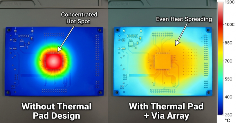
The heat from a point source is spread across large copper planes by a well-designed thermal pad system so that it is a manageable thermal profile. This helps to lower the maximum temperature of the board as well as minimize thermal gradients, which cause differential expansion. Solder joints that undergo less temperature change during thermal cycling have a great life expectancy. As mentioned in the Coffin-Manson equation in reliability engineering, a 15-20 °C change in the temperature delta can double or triple the fatigue life of a solder joint. There is no luxury for products that are required to endure for years in the field. It is a necessity.
Design Guidelines for Effective Thermal Pad Implementation
Placement, Size, and Thermal Via Coordination
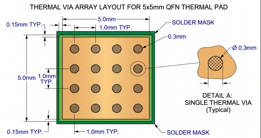
There are three decisions that need to be made when designing thermal pads: size of the landing pad, placement of thermal vias, and number of thermal vias. This is a practical solution that will be effective in most designs.
Landing Pad Size: The copper pad on the PCB should be the same size or slightly larger (5-10%) than the exposed pad of the component. However, it is possible to make it too large, which causes the component to float during reflow because of the uneven solder surface tension. If it is too small, the thermal capacity is wasted.
Thermal Via Array: Arrange an array of thermal vias in the landing pad area. Follow these guidelines:
- Apply via diameters of 0.3 mm (12 mil) for regular design or 0.2 mm (8 mil) for fine pitch application.
- Grid Space Vias with 1.0-1.2mm space between viacenters.
- To avoid solder wicking problems, vias should be at least 0.15 mm away from the pad edge.
- For a typical 5x5 mm thermal pad, use at least 5-9 vias.
- All vias to the internal ground or power plane (heat spreader).
- For optimum thermal performance and a flatter soldering surface, consider via-in-pad with filled and capped vias.
Material Selection and Thickness Considerations
The choice of PCB and thermal interface material directly influences the performance of the thermal pad system. Here are the critical factors.
Copper Weight: More copper on the inside planes equals more lateral heat spreading. Consider the use of 2 oz (70 um) copper on the internal layers in place of the usual 1 oz (35 um) for power designs. Thermal resistance decreases with increasing thickness of copper.
PCB Laminate: The standard PCB Laminate (FR4 Tg 130-140 degrees Celsius) is suitable for most applications. Use a mid-Tg (150°C) or high-Tg (170°C) laminate for designs in which the board may be exposed to temperatures above 130°C. This helps to avoid delamination and to keep mechanical integrity close to hot areas.
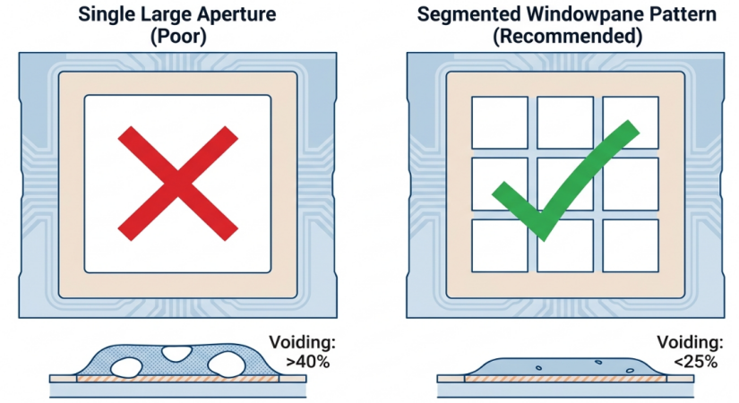
Solder Paste for Thermal Pads: Apply solder paste pattern on the thermal pad as a series of segments instead of a single large opening. One solution is to break the pad up into a grid of smaller paste pads, with 50-75% of the pad area. Controlled paste coverage limits the voiding under the component.
| Parameter | Recommended Value | Notes |
|---|---|---|
| Solder paste coverage | 50-75% of the pad area | Segmented stencil aperture |
| Via diameter | 0.2-0.3 mm | Smaller for fine-pitch |
| Via pitch | 1.0-1.2 mm | Center-to-center |
| Copper weight (internal) | 1-2 oz | 2 oz for high-power |
| Stencil thickness | 0.12-0.15 mm | Standard for QFN pads |
Thermal Interface Materials (TIMs): For external heatsinks attached to the other side of the board (via thermal vias), use a TIM that has a thermal conductivity of 1 to 6 W/mK. These include silicone thermal pads, graphite sheets, and phase change materials. This is dependent upon the compression force available and gap tolerance in your assembly.
Manufacturing Best Practices for Thermal Pad PCBs
Quality Control for Thermal Performance and Adhesion
Visual inspection is not the only way to check the quality of the thermal pad. There are a variety of inspection and testing procedures used to guarantee that the thermal connection is up to specification.
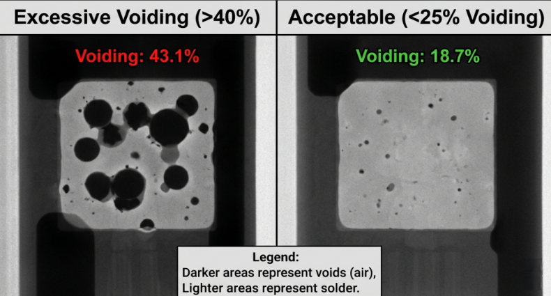
X-Ray Inspection: This is the "Gold Standard" for thermal pad solder joints. The percentage of void under the component is determined by X-ray imaging. Industry best practice is <25% voiding on thermal pads; many high-reliability applications (automotive, medical, aerospace) require <15% voiding. Too much voiding decreases the effective thermal contact area and causes insulating air pockets.
Thermal Imaging: Functional testing can be done at the board level using infrared cameras. The device's power is turned on, and the thermal profile is monitored. This will allow the engineers to ensure that heat is being distributed. The lack of solder attachment or excessive voiding will be marked by hot spots over the thermal pad.
Some of the quality checkpoints are:
- X-ray void percentage measurement (less than 25% is desired)
- Soldering - Integrity of all thermal via connections
- Filled and capped vias are planar (IPC-4761 compliant)
- Uniformity of the thickness of copper plating in thermal vias
- No Delamination or Blistering around High Temperature Area after Reflow
- JLCPCB's expertise in Thermal Pad Solutions.
JLCPCB's Expertise in Thermal Pad Solutions
Advanced Thermal Management Capabilities and Material Options
If you're looking to make PCBs with a strict thermal pad requirement, it's important to have a fabrication partner that can provide the capabilities you need. JLCPCB provides a full range of thermal management options, from basic thermal pads to elaborate multi-layer thermal solutions.
They have the capability to produce filled and capped vias for via-in-pad thermal designs, copper weights up to 2 oz on internal layers, and a wide range of laminate materials across a variety of Tg ratings. When it comes to designs that go beyond standard FR4, JLCPCB is on hand to accommodate high-Tg laminates and even metal-core PCBs (aluminum or copper substrate) for applications such as LED lighting, which have a high requirement for thermal conductivity through the board.
Reliable Production from Prototype to High-Volume Runs
From 5 prototype boards to validate a thermal design to thousands of boards for production, JLCPCB will consistently provide you with the quality you want. Starting from $2 for the PCB fabrication and $20 for SMT assembly, you can prototype your thermal pad design, validate the design with X-ray inspection and thermal testing, and then go into volume production with the same manufacturer.
This continuity is important for thermal designs because the process parameters for manufacturing, such as reflow profile, stencil specification, and via fill quality,y are consistent from prototype to production. This means that the thermal performance you test on your prototype boards will be the same on your production boards. That consistency removes a big risk factor for engineers who must work on temperature-sensitive products.
FAQ about PCB Thermal Pad
Q: What is a thermal pad on a PCB?
A thermal pad is an exposed copper area on the underside of a surface-mount component (such as a QFN or DFN package) that provides a direct thermal path from the component's die to the PCB. It is soldered to a matching copper landing pad on the board, allowing heat to flow into the PCB's copper layers and spread across a larger area for more effective dissipation.
Q: How many thermal vias should I use under a thermal pad?
The number depends on the pad size and the power being dissipated. As a general rule, use a grid of vias with 1.0 to 1.2 mm spacing. For a typical 5x5 mm thermal pad, 9 to 16 via are common. Higher power components or tighter thermal budgets may require more vias or larger via diameters to reduce the total thermal resistance.
Q: Should thermal vias be filled or left open?
For the best thermal performance and soldering reliability, filled and capped vias are recommended. Open vias can wick solder away from the thermal pad during reflow, creating voids that reduce thermal contact. If cost is a concern, solder mask tenting over the vias on the component side is a lower-cost alternative.
Q: Can I use thermal pads on a 2-layer PCB?
Yes, thermal pads work on 2-layer boards. The thermal vias transfer heat directly to the bottom copper layer, which should include a large copper pour to act as a heat spreader. While not as effective as a multilayer design with dedicated internal copper planes.
Conclusion
Effective thermal management is no longer a luxury in modern electronics; it is a fundamental requirement for system longevity. While standard FR4 substrates struggle to transfer heat efficiently on their own, the strategic implementation of PCB thermal pads changes the game. By pairing properly sized landing pads with optimized thermal via arrays—specifically maintaining a 1.0–1.2 mm pitch and controlling solder voiding to under 25%—designers can seamlessly channel destructive heat away from vulnerable semiconductor junctions.Whether your next design involves high-power LED arrays, motor drivers, or RF amplifiers, partnering with a capable manufacturer ensures these critical thermal paths are fabricated with precision. Investing the time to refine your thermal pad layouts during the prototyping phase guarantees that your high-volume production boards remain cool, reliable, and built to last in the field.
Keep Learning
Unlocking Smaller and Smarter PCBs with Embedded Components
Have you ever opened a smartwatch or a pair of wireless earbuds, looked at the miniature chip inside, and wondered how engineers could pack so much functionality into such a small enclosure? While surface-mount technology (SMT) has become incredibly sophisticated—with the advent of ultra-small 0201 and 01005 packages—there is a physical limit to how many components can be crammed onto the surface of a board. To bypass this bottleneck, the electronics manufacturing industry is increasingly turning to e......
Improving Heat Dissipation : The Smart Use of Thermal Pads in PCB Design
Key Takeaways Optimizing PCB thermal pad design and via arrays is essential to prevent semiconductor failures caused by FR4's low thermal conductivity. By implementing a 1.0–1.2 mm via pitch and keeping solder voiding below 25% through segmented stencils, designers can eliminate localized hot spots and boost board reliability from prototype to high-volume production. Have you ever considered that the thermal conductivity of a normal FR4 PCB is only about 0.3 W/mK? That is an acceptable number for low-......
Comparison of BGA vs LGA in High-Power Applications
Key Takeaways In high-power PCB designs, BGA and LGA packages offer strong high I/O performance but require effective thermal management. BGA excels with solder balls and thermal vias, while LGA relies on direct pad contact with TIMs and thermal pads. Key to success are thermal vias, thicker copper layers, ground planes, and simulations to reduce thermal resistance and maintain reliable junction temperatures. As electronic devices continue to shrink in size while increasing in performance, managing he......
A Complete Guide to IC Package: Types, Properties, PCB Design Rules & Selection Tips
What is an IC Package? An IC package is the physical enclosure that houses an integrated circuit or electronic component, providing mechanical protection, electrical connections, and thermal management. It ensures that the component can be reliably mounted on a PCB and integrated into circuits. Key Functions of an IC Package: 1. Mechanical protection: Shields the chip from physical damage and environmental factors. 2. Electrical connections: Provides pins or solder balls to connect the IC to the PCB. ......
BGA vs LGA: Understanding the Differences and Choosing the Right Package
In the world of electronic components, the choice of package type plays a crucial role in the overall performance, reliability, and manufacturability of a printed circuit board (PCB). Two popular package types that are widely used in modern PCB design are BGA (Ball Grid Array) and LGA (Land Grid Array). Understanding the differences between these two packages is instructive for electronics enthusiasts, hobbyists, engineers, students, and professionals in the field of electronics and PCB design. This a......
Technical Guidance: BGA Design Rules
With the advancement of the electronics industry, chip integration continues to increase, the number of IO pins quickly rises, and power consumption grows accordingly, leading to stricter requirements for integrated circuit packaging. To meet the demands of this progress, Ball Grid Array (BGA) packaging technology is introduced. This technology involves the creation of an array of solder balls on the bottom of the package substrate as the I/O interface for the circuit, connecting it to the printed cir......