How PCB Functional Testing Ensures Your Product Works Flawlessly from Day One
13 min
- Why Functional Testing Matters More in Modern Electronics
- Understanding PCB Functional Testing (FCT) and How It Differs from Other Methods
- Common PCB Testing Strategies and When to Deploy Full FCT
- How JLCPCB's High-Precision Inspection Lays the Foundation for Successful FCT
- Best Practices for Designing PCBs Ready for Functional Testing
- FAQ about PCB Functional Testing
- Conclusion
Key Takeaways
- Looks right doesn’t mean it works right. Only PCB Functional Testing (FCT) verifies real-world performance that structural tests like AOI, ICT, and X-ray cannot catch.
- JLCPCB’s E-test, AOI, and X-ray ensure zero-defect hardware, so your FCT focuses on design and firmware issues.
- Design for testability: add clear test points and include a firmware test mode for fast verification.
- Final Tip: Always perform FCT before shipping — it prevents expensive field failures and builds product confidence from day one.
A few years ago, I sent off some motor-driver boards that I had given the visual test on the bench, and they all checked out. The solder was clean, the assembly house signed off on AOI, and all the panels came with no cosmetic issues whatsoever. So I started the first one on their line and watched it sit, there doing nothing. The product had perfect hardware, but did not work. That hurt, and it was a lesson that I tell every client: Don't mistake a board that looks right for a board that behaves right. You can only find out whether your design really works by putting it to the test and comparing it to the spec, end to end.
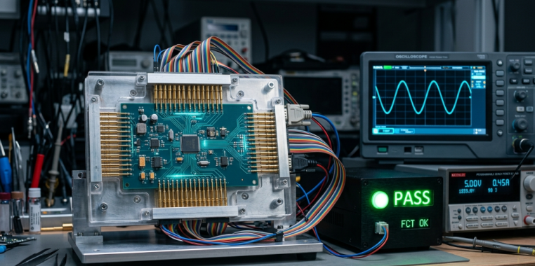
The step is PCB Functional Testing, and not taking it is how you can make a great fabrication run into a field failure nightmare. In this guide, I would like to give you a first-hand tutorial for functional testing as I do and use it in real production. We will discuss the importance of PCB FCT more than ever, how it differs from ICT, AOI, flying probe, and X-ray, what equipment is required, and how to design a board that tests with ease. I will also be frank with you and tell you where your fabricator's work stops and where yours begins: clean inspection upstream means painless FCT downstream.
Why Functional Testing Matters More in Modern Electronics
Electronics are becoming denser, faster, and more firmware-dependent, and it's done a number on testing without you noticing it. A modern board is not only copper and components; it's a software-based system where if one register is set wrong, or one supply rail is a little too close to its limits, the whole thing can fail in the field. That's the type of failure that can be detected only by visual and structural inspections. The only time the board is used for its end purpose is during functional testing when it runs under power and performs its function. Hence, it's no longer a nice-to-have but rather a standard requirement for anyone sending out real volume.
The Hidden Risks of Skipping PCB FCT
If you don't do functional verification, you're assuming that all the upstream processes were done perfectly, and that you have no behavioral bugs in your design. That bet doesn't come through on a complex board as frequently as you would like to think. The failures that get through are typically the costly, not-easily-followed varieties.
- Faults in the firmware and configuration that cannot be detected by optical or physical testing.
- A regulator that maintains a constant temperature at light load but drops at heavy load is called marginal performance.
- Connectivity that is sometimes present, but not present when the board is actually running, when using a static probe
- Stacking up components that cause a circuit to just barely exceed the operating limit.
- Field returns and brand damage are costs that far exceed those of a test fixture.
The harsh reality is that a defect found at FCT may be a few dollars to fix, but the same defect found by your customer can result in hundreds of dollars of rework, shipping, and reputation.
Understanding PCB Functional Testing (FCT) and How It Differs from Other Methods
There is some confusion about the usage of the term 'testing' as it is used as one thing, whereas in fact, board-level testing is a group of methods, each of which is focused on a particular slice of the problem. What matters is the understanding of where FCT needs to fit in that family.
What Is PCB Functional Testing?
PCB Functional Testing (FCT) involves powering on a completed Assembly and testing whether it functions as per the functional specification. An FCT test is designed to test the board as a whole working system, like the end user experiences it, rather than for individual components or solder joints.
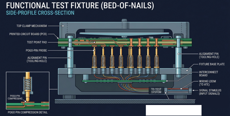
In practice, the board is plugged into a test fixture via its edge connector, a bed-of-nails, or a custom interface harness. The fixture supplies power, input signals or commands, and determines the outputs. Firmware is commonly loaded first, and then the test sequence is run on the board to ensure that all of the board's functions voltages, communication buses, sensors, motor outputs, LED states etc.
PCB FCT vs. ICT, AOI, and Flying Probe – A Quick Comparison
Every approach has a sweet spot, and the wise thing to do is to combine them all. AOI, X-ray catch build of the board, ICT, flying probe catch the correctness of the connections and parts, FCT catch the working of the product. Let's take a look at the most common PCB testing methods.
| Method | What It Checks | Board Powered? | Fixture Needed | Best For |
|---|---|---|---|---|
| Functional Test (FCT) | End-to-end behavior vs. spec | Yes | Yes (custom/bed-of-nails or edge connector) | Verifying the finished product actually works |
| In-Circuit Test (ICT) | Component values, shorts, and opens at the part level | Partly | Yes (bed-of-nails) | High-volume structural and component verification |
| AOI (Optical) | Solder joints, placement, polarity, and presence | No | No | Catching visible assembly defects fast |
| Flying Probe | Opens, shorts, component presence | Partly | No (moving probes) | Low/mid volume and prototypes, no fixture cost |
| X-Ray (AXI) | Hidden joints under BGA/QFN, voids, internal layers | No | No | Inspecting solder, you cannot see it optically |
Common PCB Testing Strategies and When to Deploy Full FCT
Overview of Popular Board-Level Testing Methods
Typically, production test plans employ a structural and a functional approach. The structural side is to provide assurance that the board was put together correctly, and the functional side is to provide assurance that the board works. Some of the techniques I gravitate towards:
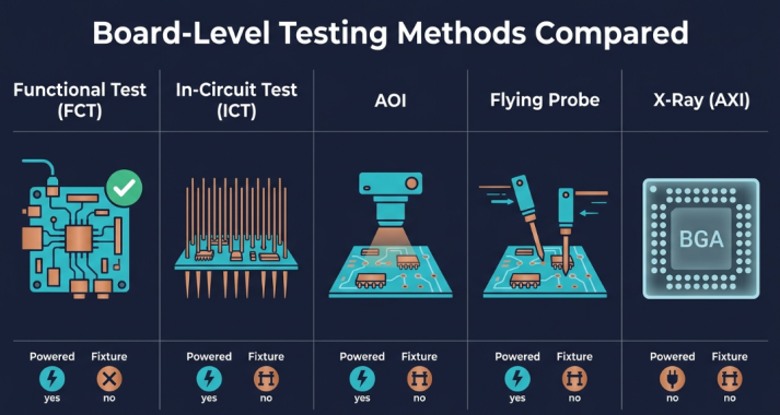
- AOI + FCT: The industry staple for most consumer and industrial boards, to identify visible defects and then substantiate functionality.
- AOI + X-ray + FCT: For BGAs or bottom-terminated parts, where hidden joints need to be confirmed.
- Flying Probe + FCT: Prototype and low volume: Verifies connections and behavior, avoids fixture cost.
- Boundary scan (JTAG) + FCT: For dense digital boards where physical probe access is limited, and JTAG can reach buried nets.
The idea is that FCT is almost invariably the last link in the chain. Structural tests reduce the number of failures to the point where, in a functional test, the behavior is being verified, not solder failures.
Identifying When Your Project Requires Complete FCT Verification
So, when is full FCT a non-negotiable? Well, if I've learned anything in my life, it's that the answer is "more often than people like to think. Any board with firmware on it that controls something physical or has any safety implications should always receive functional verification. Triggers I am alert to:
- The board is running firmware, or there's some behavior it has that can't be tested structurally.
- It powers real-world loads such as motors, power stages, RF, and high-current rails.
- Safety, medical, automotive, or regulatory requirements that require documentation.
- It blends the analog and digital world where margins count.
- Failure in the field is much more expensive than a test fixture.
How JLCPCB's High-Precision Inspection Lays the Foundation for Successful FCT
Rigorous Bare-Board E-Test and AOI Eliminating Fabrication Defects
JLCPCB performs bare-board electrical test (flying probe or fixture E-test) on the fabricated PCB before the placement of any components. This is to make sure that all nets are checked for opens and shorts versus the netlist, and that you will never have a broken trace or an etched-away connection due to the fabrication process. During manufacturing, automated optical inspection verifies trace integrity, solder mask registration, and quality of pads. Once the board comes out of bare-board fabrication, the copper you designed becomes the copper you have, so if it fails at FCT, it's not a phantom fabric defect; it's a design and/or firmware fault.
Advanced X-Ray and PCBA Inspection: Preventing Hidden Assembly Issues
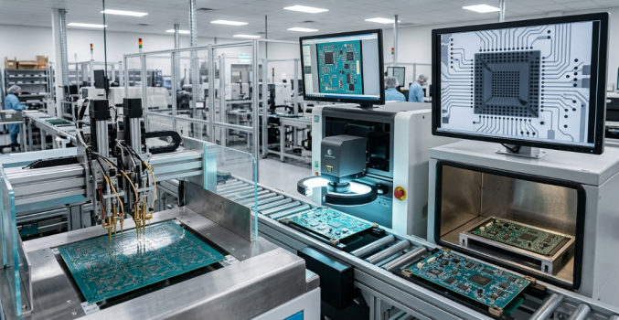
Once assembled, the inspection is even more detailed. AOI inspects the assembled board for placement, polarity, and solder-joint quality, and X-ray inspection peers straight through the BGAs, QFNs, and bottom-mounted parts where you can't see the hidden voids, bridges or opens, even with an optical system. This is of huge importance for FCT troubleshooting. A cold joint under a BGA can result in an intermittent functional failure, which may require hours to be chased on the bench. They are able to capture it at PCBA inspection, which means that JLCPCB ensures that the board delivered to your functional testing is structurally correct. Therefore, when you power it on, you are testing your design, not the assembly itself.
Minimizing FCT Troubleshooting Through Zero-Defect Hardware Delivery
The effect of E-test, AOI, and X-ray is cumulative: there will be fewer surprises at the functional test. Once the incoming hardware is found to be defect-free, your FCT pass rate rises, your debugging time decreases, and the failures that you get are clear, unambiguous, and unambiguously due to design or firmware, not manufacturing noise.
This is the proper 'division of labor'. JLCPCB's rapid quoting, low-cost prototyping, and SMT assembly mean you'll have a structurally perfect board; you perform the functional test that verifies that it does its job. The single largest lever you have to pull for your own FCT to go smoothly is to start with rigorously inspected zero-defect hardware.
Best Practices for Designing PCBs Ready for Functional Testing
Test Point Placement and Accessibility Tips for Test Fixtures
The fixture can only measure what it can physically reach, so test points are your interface to the whole test process. Do not think of them as "leftovers" but as first-class design objects. Some "rules" that I use on all the boards:
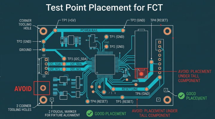
- Put test points on critical nets (power, ground, communication buses, reset, and critical analog nets.
- Round, exposed pads with a diameter of 0.9-1.0 mm or greater are ideal for making good pogo-pin contact.
- Where possible, place test points on one side of the board to facilitate a single-sided fixture.
- Keep probes from crowding by maintaining adequate spacing (~2.0 mm / 0.075" pitch).
- Offer good tooling holes and good fiducials for repeat fixture alignment.
- Don't put test points under height components or too near the board edge.
The difference between a fixture that drops cleanly and one that requires constant fixture rework to achieve contact is good test-point planning.
Firmware and Software Considerations for Smooth FCT Execution
The other half of testability is in the firmware. Even the best board in the world, if you don't have any hooks in the behavior of the software, it will do a poor test. Include a test mode in your firmware from the beginning. A dedicated test routine can switch all outputs, read all sensors, test all communication buses, and report results via serial or JTAG link — converting a multi-minute manual probe around to just a few seconds of automated verification. Combined with boundary-scan (JTAG) capability on dense digital boards, nets can be accessed that were previously unattainable by physical probes. Develop the fixture concurrently with firmware development, and the FCT is quick, repeatable, and truly reliable.
FAQ about PCB Functional Testing
Q: What is PCB functional testing, and what does it verify?
PCB functional testing (FCT) powers up a finished assembly and verifies that it behaves according to its functional specification, exercising the board as the end product would experience it. The test verifies real behavior voltages, communication, sensor, and output performance.
Q: What is the difference between functional testing and in-circuit testing (ICT)?
ICT uses a bed-of-nails to check individual components and connections at the part level, confirming values, shorts, and opens. FCT instead powers the whole board and verifies end-to-end behavior, so it catches firmware and system-level faults that a structurally perfect board could still have.
Q: Does JLCPCB perform functional testing on my boards?
No. JLCPCB does not run functional testing; FCT is performed by you or a dedicated test house against your product spec. JLCPCB provides high-precision inspection — bare-board electrical test, AOI, and X-ray — that delivers zero-defect hardware so your own functional testing goes smoothly.
Q: What equipment do I need to run PCB FCT?
At minimum, you need a test fixture (bed-of-nails, pogo pins, or mating edge connector), a programmable power supply, a test controller running the test script, and instruments like a DMM or oscilloscope to measure outputs. A firmware programmer or JTAG interface is also common for flashing and boundary-scan verification.
Q:How do I design a PCB to make functional testing easier? 2
Add accessible test points on critical nets using ~1 mm exposed pads with adequate spacing, keep them on one side, and include tooling holes and fiducials for fixture alignment. On the firmware side, build a dedicated test mode that toggles outputs and reports readings so the fixture can verify behavior quickly and repeatably.
Conclusion
If there's one thing I want you to take away from this post, it's this: looks right doesn't equal works right, and only functional testing helps fill this gap. While a Structural Test (AOI, ICT, X-ray, flying probe, etc.) will show that the board was built correctly, a PCB Functional Test is where the test determines whether the product is going to function under power. Use them wisely, plan for testing from the beginning, and your product will ship with a smile on your face, not crossed fingers.
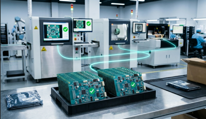
The smoother route to that confidence is upstream once your hardware has been verified by rigorous bare-board E-test, AOI, and X-ray. The kind of high precision inspection that JLCPCB embeds in every fabrication and assembly run. Your own FCT has so much less to troubleshoot and so much more to validate. Receive boards with no defects, perform a well-planned functional test, and your product is flawless from day one.
Keep Learning
How Copper Foil Shapes PCB Performance and Manufacturing Quality
Key Takeaways Weight: 1 oz copper ≈ 35 µm thickness; higher weight increases current capacity. Types: ED for standard rigid boards, RA for dynamic flex circuits. DFM & Loss: Smoother foil lowers RF loss; thicker foil requires wider trace spacing. The part of a PCB that actually carries the electrical signal is the copper foil. The strength comes from the glass weave, the resin is used to keep the layers together, and the solder mask is used to provide protection and separation of exposed copper. But w......
A Complete Guide to Copper Clad Laminate (CCL) in PCB Manufacturing
Key Takeaways CCL is the base material: a cured resin-reinforcement sheet with copper foil bonded to one or both sides. Three parts control performance: Resin affects heat and loss, reinforcement controls stability, and copper foil affects conductor behavior. Choose by the main design stress: Heat, frequency, and cost usually determine the best laminate family. Slash sheets define the material: IPC-4101 uses numbered slash sheets to specify rigid PCB base materials. Tg alone is not enough: Td and time......
Buried Vias in Advanced PCBs: Enabling Higher Density, Better Signal Integrity, and Compact Designs
Key Takeaways Hidden Routing: Buried vias connect only inner layers, keeping outer surfaces clear for dense components and traces. Better Signal Integrity: They eliminate via stubs, reducing parasitics and signal loss in high-speed designs. Higher Density: Essential for HDI boards, dense BGAs, and small form factors like wearables. Higher Cost: Sequential lamination and extra drilling steps make them ~3×-4× more expensive than standard through-holes. Ever wondered how a modern smartphone mainboard can......
Unlocking Higher Density and Better Performance with Blind Vias in HDI PCBs
Key Takeaway Higher Density: Connects surface to inner layers without penetrating the whole board, freeing routing channels under fine-pitch BGAs. Improved Signal Integrity: Reduces via stub length to minimize impedance discontinuities in high-speed designs. Aspect Ratio Rule: Keep the depth-to-diameter ratio near 0.75:1 (max 1:1) for reliable laser drilling and void-free plating. Thermal Efficiency: Supports via-in-pad setups for better heat dissipation and compact component placement. Ever wonder ho......
How to Select Tg of PCB ?
What is the Tg of PCB? In PCB manufacturing, "Tg" stands for Glass Transition Temperature. It is the temperature at which the PCB substrate material transitions from a rigid, glassy state to a soft, rubbery state. PCBs are flame-retardant (UL94 V-0) and do not burn easily; instead, they soften above Tg. The Critical Correlation Between Tg and Z-Axis CTE (Coefficient of Thermal Expansion) When the temperature exceeds the Tg point, the PCB substrate material (such as standard FR-4) undergoes a physical ......
Beyond the Basics: The Role of PTFE PCBs
Polytetrafluoroethylene (PTFE) PCBs are integral to advanced electronic applications. Among various PCB materials, Teflon, the brand name for Polytetrafluoroethylene (PTFE). Teflon PCBs, known for their high frequency and heat resistance properties. All of this is achievable due to its exceptional dielectric properties. RF PCB designs often make use of low-loss PTFE-based materials thanks to their very low dielectric losses and huge range of possible Dk values. Low Dielectric Constant: Enables high-sp......