Understanding Impedance Formulas for Accurate PCB Design
15 min
- What Is Electrical Impedance?
- Essential Impedance and Reactance Formulas
- How to Calculate Impedance in Different Circuits
- Using Impedance Calculators for Faster Design
- Applying Impedance Formulas to PCB Design and Manufacturing
- FAQs about Impedance Formulas
- Conclusion
- Complex Impedance: Z = R + jX combines constant resistance with frequency-dependent reactance.
- Frequency Behavior: Inductive reactance rises with frequency while capacitive reactance falls.
- Circuit Rules: Impedances add directly in series, while parallel networks sum admittances (Y = 1/Z).
- Trace Impedance (Z0): Depends on cross-section and dielectric properties, not trace length.
- Stackup Verification: Always confirm calculated trace widths with your fabricator's stackup and solder mask data.
An impedance formula determines the extent to which a circuit element, network, or PCB trace resists the flow of alternating current at a specific frequency. Resistors, capacitors, and inductors have a very simple relationship. It is the combination of these that forms filters, decoupling networks, and resonant circuits, and this combination determines the impedance. The same concept applies to the characteristic impedance of a trace, which determines whether a fast edge arrives cleanly or is reflected off the board.
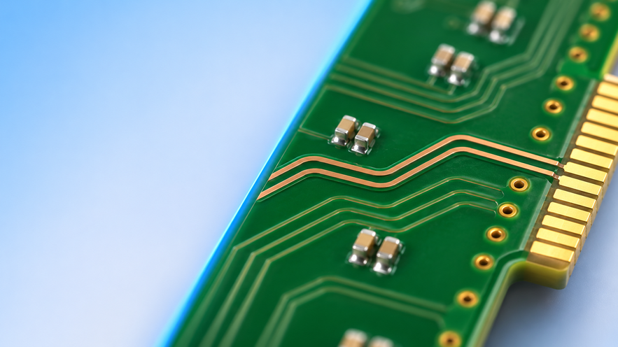
Figure 1: Controlled-impedance traces routed over a reference plane on a multilayer PCB
This article will discuss the basic equations for calculating impedance and reactance; how to calculate them for RC, RL, and RLC circuits; the inputs to an impedance calculator; and how stackup and trace geometry determine the impedance of a fabricated PCB.
What Is Electrical Impedance?
Electrical impedance is the total opposition that a component or circuit offers to alternating current, expressed in ohms. It is not resistance; it affects the timing of the current relative to the voltage, not its resistance.
Resistance, Reactance, and Impedance Explained
Resistance is the conversion of electrical energy into heat, and it is the same at all frequencies. The current through a resistor is directly proportional to the voltage across the resistor. Reactance is the opposition from parts that store energy rather than dissipate it. It is stored in a magnetic field by an inductor and an electric field by a capacitor. Their current and voltage are 90° out of phase, and each returns that energy to the circuit every cycle.
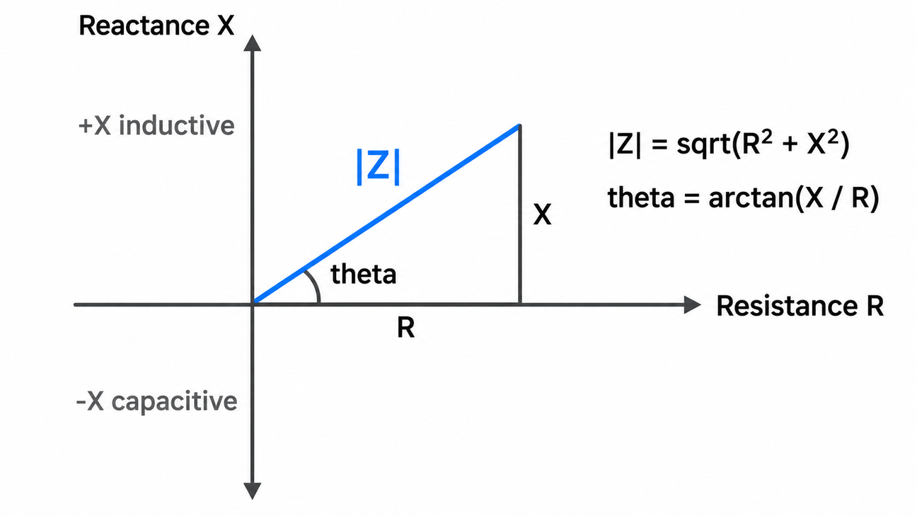
Figure 2: The impedance triangle: resistance, reactance, and the magnitude and phase of Z
Impedance is the combination of the two into a single complex number. Resistance is the real part, reactance is the imaginary part, and the result is a magnitude (in ohms) and phase angle. The magnitude indicates the amount of current that will pass for a given voltage. The phase angle indicates how much the current leads or lags the voltage, which is important for filters, power factor, and the stability of feedback loops.
How Frequency Affects Electrical Impedance
Frequency affects impedance because reactance depends on the rate of change of current. The inductor resists changes in current, and the higher the signal frequency, the greater the resistance. Thus, its impedance increases with frequency. A capacitor requires time to charge, so the higher the frequency, the more current it can pass for a given voltage, and the lower its impedance.
This is because a single component may behave differently throughout a design. A blocking capacitor is a very short circuit to a 100 MHz noise source, while a small inductor, which appears as a short circuit at 1 kHz, can choke a fast switching edge. It also implies that, without the frequency, any impedance value is incomplete. The 600 Ω listed in a ferrite bead datasheet is measured at a single frequency, usually 100 MHz, and at DC the bead's impedance is close to its small series resistance.
Essential Impedance and Reactance Formulas
Most circuit work is done using three formulas: the complex impedance formula, the two reactance formulas, and the series-and-parallel formulas. They are valid for any linear passive network since the impedance of each network element is a function of the value and frequency.
The Basic Impedance Formula
In the basic impedance formula, impedance is represented as a complex number: Z = R + jX. In this case, Z is the impedance, R is the resistance, X is the reactance, and j is the imaginary number (j2 = −1). Engineers use j instead of i because i is already used for current. If X is positive, it is inductive, and if X is negative, it is capacitive.
The magnitude and phase are derived from the same triangle used to derive the magnitude and phase of any complex number: |Z| = √(R² + X²) and θ = arctan(X/R). Impedance also follows the AC form of Ohm's law, Z = V/I, where V and I are phasors and so have both amplitude and phase. So a load with R = 30 Ω and X = 40 Ω has |Z| = 50 Ω, and its current lags the voltage by 53°.
Inductive and Capacitive Reactance Formulas
The two reactance formulas give the size of X for an inductor and a capacitor, using the angular frequency ω = 2πf, where f is in hertz.
| Element | Impedance | Reactance Formula | Behavior with Rising Frequency |
|---|---|---|---|
| Resistor | Z = R | none (X = 0) | Constant |
| Inductor | Z = jωL | XL = 2πfL | Rises in proportion to f |
| Capacitor | Z = 1/(jωC) = −j/(ωC) | XC = 1/(2πfC) | Falls in proportion to 1/f |
The capacitor's impedance carries a minus sign because 1/j = −j, which is what places capacitive reactance below the axis in the impedance triangle. When a formula combines both elements, the net reactance is X = XL − XC, with both terms entered as positive magnitudes.
The proportionality is what makes the formulas useful for quick estimates. A 10 nH inductance is 0.63 Ω at 10 MHz and 6.3 Ω at 100 MHz, while a 100 nF capacitor is 0.16 Ω at 10 MHz and 0.016 Ω at 100 MHz.
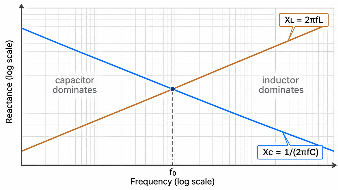
Figure 3: Inductive reactance rises with frequency while capacitive reactance falls
Impedance Formulas for Series and Parallel Circuits
Impedances combine with the same rules as resistors, provided you keep them complex. In series, the same current flows through every element, so the impedances add: Z = Z1 + Z2 + Z3. The real parts add to give total R, and the imaginary parts add to give total X, which is how an inductor's positive reactance can cancel a capacitor's negative one.
In parallel, the same voltage appears across each element, so the currents add, and the reciprocals sum: 1/Z = 1/Z1 + 1/Z2 + 1/Z3. The reciprocal of impedance is admittance, Y = 1/Z, measured in siemens. Many engineers switch to admittance for parallel networks because the arithmetic becomes a plain sum. For two elements, the shortcut Z = Z1Z2/(Z1 + Z2) still applies, but only when the multiplication and division are done as complex numbers.
How to Calculate Impedance in Different Circuits
The impedance formulas by circuit type all follow from the series and parallel rules. Each one is a substitution rather than a new formula to memorize.
RC and RL Circuit Impedance
A series RC circuit has Z = R − j/(ωC), so |Z| = √(R² + XC²). At low frequency, the capacitor dominates, and the impedance is large. At high frequencies, the capacitor's reactance decreases, and the impedance approaches R. The crossover, where XC = R, occurs at the corner frequency fc = 1/(2πRC). At that point, |Z| = R√2 and the phase is −45°. This is the same frequency that sets the −3 dB point of an RC low-pass or high-pass filter.
A series RL circuit is the mirror image: Z = R + jωL, with |Z| = √(R² + XL²) rising with frequency, and a corner at fc = R/(2πL) with a phase of +45°. A parallel RC circuit behaves the other way round, with Z = R/(1 + jωRC). Its impedance equals R at DC and falls once the capacitor starts to conduct. That is how a filter capacitor across a sensor's load resistor shunts noise to ground.
RLC Circuit Impedance
A series RLC circuit has Z = R + j(ωL − 1/(ωC)), so its magnitude is |Z| = √(R² + (XL − XC)²). The two reactances cancel at the resonant frequency f0 = 1/(2π√(LC)). At f0, the impedance falls to its minimum, R alone, and the current is in phase with the voltage. Below f0, the circuit is capacitive, and above it, inductive.
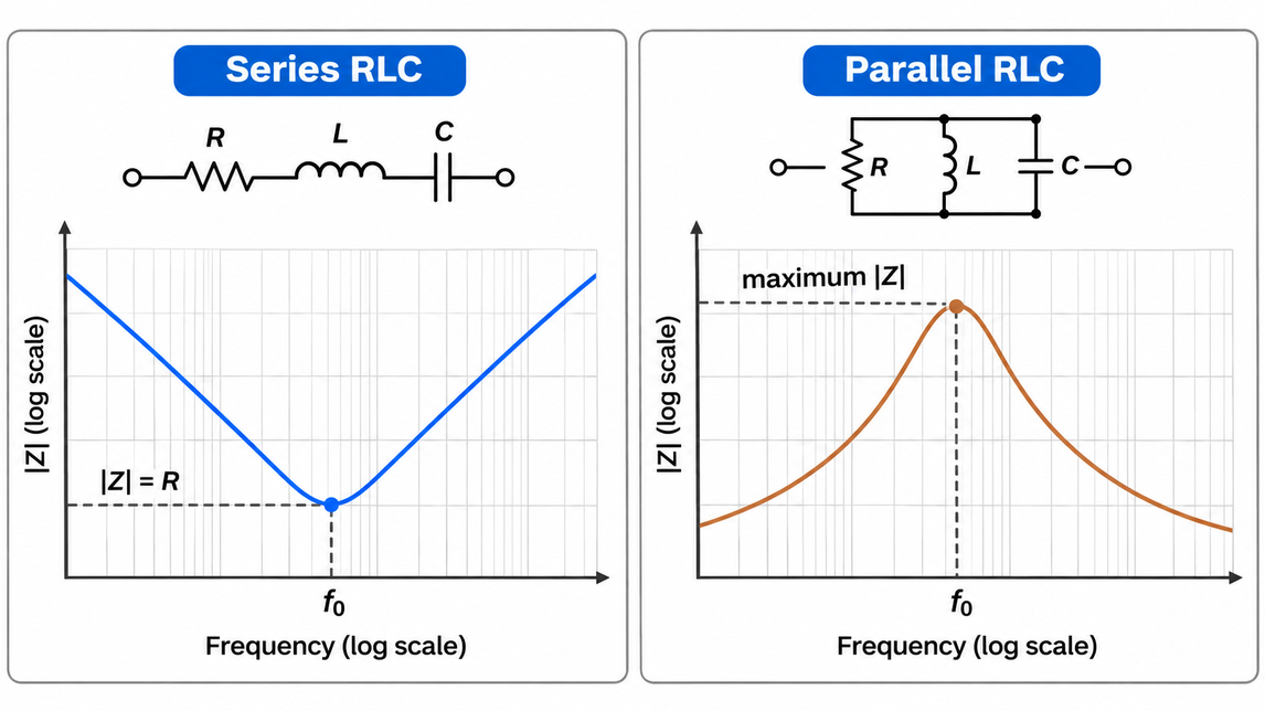
Figure 4: Series RLC impedance dips to R at resonance; parallel RLC impedance peaks
A parallel RLC circuit resonates at the same f0, but its impedance there is a maximum. The admittance is 1/Z = 1/R + j(ωC − 1/(ωL)), and at f0 the inductive and capacitive currents cancel, leaving only the resistor's admittance. How sharp each curve is depends on R. In a series circuit, a smaller R gives a deeper, narrower dip, while in a parallel circuit a larger R gives a taller, narrower peak.
Impedance in AC and High-Frequency Circuits
At higher frequencies, every real component becomes an RLC circuit. Its leads, pads, and internal structure add parasitic inductance and capacitance. A decoupling capacitor is the clearest case. Its package and mounting add series inductance, so it is a series RLC circuit with a self-resonant frequency, above which it behaves as an inductor.
Take a 100 nF capacitor and assume a total series inductance of 1 nH from its package, pads, and vias. The series resonance formula gives f0 = 1/(2π√(1 nH × 100 nF)) ≈ 15.9 MHz. At 100 MHz, the capacitive reactance is only 0.016 Ω, but the inductive reactance is 0.63 Ω, so the part acts as a small inductor. Shorter mounting lowers the inductance and moves the resonance up.
Resistance changes too. Skin effect pushes high-frequency current toward the conductor surface. In copper, the skin depth is about 65 µm at 1 MHz and about 2.1 µm at 1 GHz, so once the skin depth falls below the copper thickness, a trace's AC resistance rises well above its DC value.
Using Impedance Calculators for Faster Design
Impedance calculators remove the arithmetic. Each one still returns a number only as good as its formula and its inputs.
How an Impedance Calculator Works
There are two kinds. A circuit impedance calculator takes R, L, C, and frequency, and applies the formulas in this article directly to return magnitude and phase. A PCB trace impedance calculator works with geometry instead. It takes trace width, copper thickness, dielectric height, and dielectric constant, then computes the characteristic impedance or solves backward for the width that meets a target.
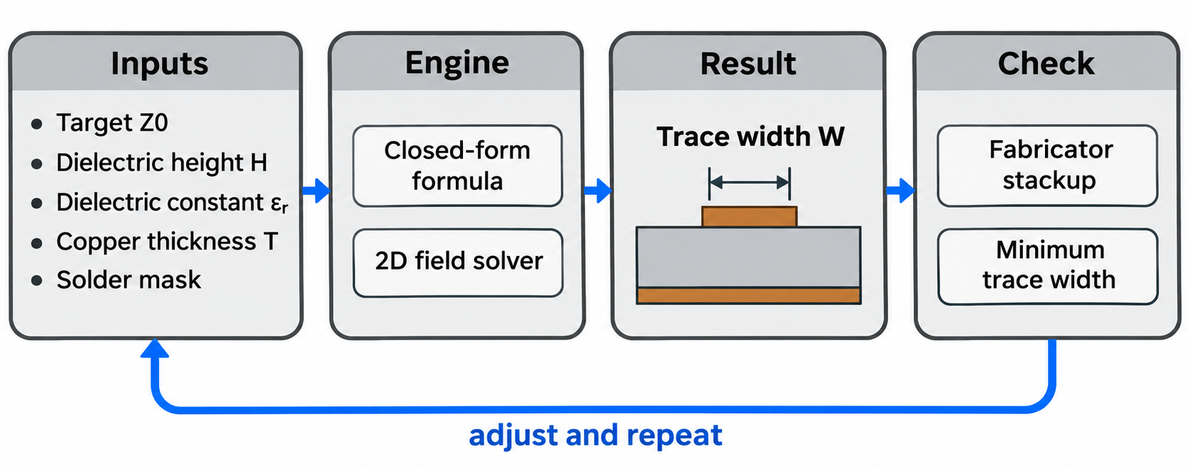
Figure 5: How an impedance calculator turns stackup inputs into a trace width
Trace calculators differ in their engine. Many online tools use closed-form approximations such as the IPC-2141 equations or Wadell's equations. Of the two, Wadell's are generally rated the more accurate for microstrip. Others use a 2D field solver that models the actual cross-section, including solder mask and a trapezoidal etched profile. Most closed-form formulas are lossless, so they treat impedance as constant across frequency and lose accuracy as frequency approaches the gigahertz range.
Key Inputs and Results to Check
The inputs below set the answer, so each one should come from the board that will be built rather than from a default.
| Input | What It Changes | Where to Get It |
|---|---|---|
| Dielectric height (H) | Distance to the reference plane; Z0 rises with H | Fabricator's stackup |
| Dielectric constant (εr) | Field strength in the laminate; Z0 falls as εr rises | Prepreg or core value, not a generic FR-4 figure |
| Trace width (W) and thickness (T) | Conductor size; Z0 falls as either grows | Design rules and finished copper weight |
| Solder mask | Raises effective εr and lowers outer-layer Z0 | Mask thickness and Dk from the fabricator |
| Structure type | Microstrip, stripline, coplanar, differential | Layer and reference planes in the layout |
On the result side, check that the computed width is above the fabricator's minimum trace width for that copper weight. Then confirm that the geometry sits inside the formula's valid range. For a differential pair, the calculator should report differential impedance, not single-ended impedance.
Applying Impedance Formulas to PCB Design and Manufacturing
On a PCB, the impedance formula that matters for fast signals is characteristic impedance, a property of the trace's cross-section. It explains the broader role of impedance in PCB design: a trace is a distributed circuit once its delay becomes comparable to the signal's rise time.
Characteristic Impedance in PCB Transmission Lines
A long trace over a plane is a chain of tiny series inductances and shunt capacitances. Its characteristic impedance is Z0 = √((R + jωL)/(G + jωC)), where R, L, G, and C are per unit length. For a low-loss line at high frequency, R and G become small next to ωL and ωC, so Z0 ≈ √(L/C). That is why Z0 has no length term: a longer trace adds inductance and capacitance in the same ratio.
A signal travels at v = c/√εeff, where εeff is the effective dielectric constant. For a stripline in FR-4 with εr = 4.4, that is about 143 mm/ns, or roughly 7 ps per millimeter. When the edge sees a change in Z0, part of it reflects with a coefficient Γ = (ZL − Z0)/(ZL + Z0). A 50 Ω line into a 75 Ω load reflects 20% of the incident voltage. That is the problem impedance matching and controlled-impedance routing exist to prevent.
How PCB Stackup and Trace Geometry Affect Impedance
The stackup sets the dielectric height and constant, and the layout sets the width. For an outer-layer microstrip, the IPC-2141 approximation is Z0 = 87/√(εr + 1.41) × ln(5.98H/(0.8W + T)). It holds roughly for W/H between 0.1 and 2.0. For a centered stripline between two planes spaced B apart, it is Z0 = 60/√εr × ln(1.9B/(0.8W + T)), for narrow traces up to about W = 0.35B. IPC no longer maintains IPC-2141A, but its equations remain the common first estimate.
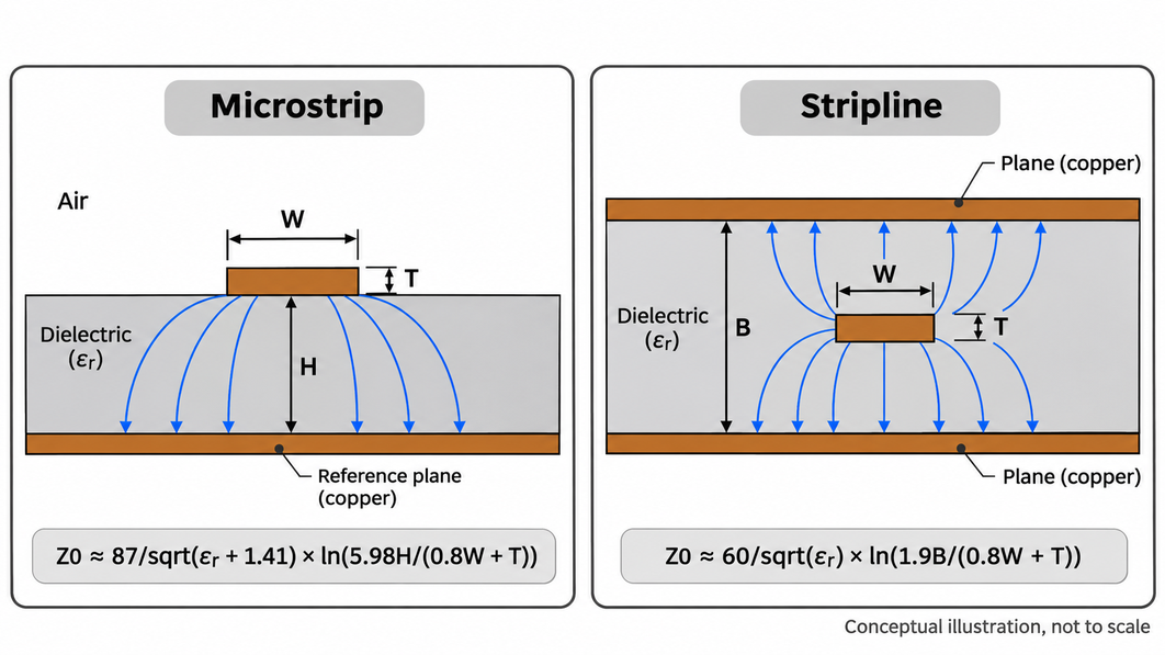
Figure 6: Microstrip and stripline cross-sections with the dimensions the formulas use
For a worked case, take an outer layer over 0.2104 mm of 7628 prepreg with εr = 4.4 and 0.035 mm copper. Solving for 50 Ω yields W ≈ 0.35 mm (13.8 mil), with W/H = 1.66, which is within the range. That is an estimate before solder mask, which lowers the impedance, so a calculator that models the mask typically returns a slightly narrower width.
The logarithm makes the sensitivity easy to see. On that line, a 10% thicker dielectric raises Z0 by about 3.4 Ω, and a 10% wider trace lowers it by about 3.1 Ω, while a ±10% tolerance band is only ±5 Ω. Stackup thickness and etch control, not the formula, set most of the error. The formula is only as good as the stackup values entered into it.
Controlled Impedance PCB Manufacturing at JLCPCB
The formulas give a design target, and the fabricator's stackup decides whether the board meets it. JLCPCB offers impedance control on 4- to 32-layer boards, with a standard tolerance of ±10% and ±5% on special request. For 4- and 6-layer boards, it publishes named impedance stackups, such as JLC04161H-7628. Each lists every copper, prepreg, and core thickness with its dielectric constant, and the board is produced to the selected stackup.
That published data supplies the H, T, and εr the formulas need, plus a solder mask Dk of 3.8 and its coating thickness. The impedance calculator then computes trace widths for each target and recommends stackups, listing the one with the lowest cost and quickest turnaround first. Once the widths are in the layout, upload your Gerber files to get an instant quote.
FAQs about Impedance Formulas
Q: What is the unit of impedance?
The ohm (Ω), the same unit as resistance, because impedance is a ratio of voltage to current. Its reciprocal, admittance, is measured in siemens (S), and its real and imaginary parts are called conductance and susceptance.
Q: Can impedance be negative?
Reactance can be negative, because a capacitor's reactance carries a minus sign in Z = R + jX. The resistive part of a passive component is never negative, since a passive part cannot supply energy. Negative resistance appears only in active circuits such as oscillators.
Q: Does trace length change characteristic impedance?
No. Characteristic impedance depends on the trace's cross-section: width, copper thickness, dielectric height, and dielectric constant. Length changes the propagation delay and the total loss, so a long line attenuates more, but its Z0 stays the same along a uniform section.
Q: What is the difference between single-ended and differential impedance?
Single-ended impedance is one trace measured against its reference plane. Differential impedance is measured between the two traces of a pair driven at opposite polarities and equals twice the odd-mode impedance. Closer spacing increases coupling and lowers impedance.
Q: How is impedance measured on a PCB?
Components are measured with an LCR meter or impedance analyzer at a set frequency. Trace impedance is usually measured by time-domain reflectometry (TDR) on a test coupon that replicates the trace geometry, thereby showing impedance along the line as a function of distance.
Conclusion
Impedance formulas reduce to a few rules: Z = R + jX, XL = 2πfL, XC = 1/(2πfC), series impedances add, and parallel admittances add. For PCB traces, the closed-form equations provide a reliable initial width estimate, but stackup values and solder mask determine the final result. The decision rule is to calculate by hand for understanding, then confirm every controlled trace with the fabricator's own stackup data before release. When the widths match the stackup, order your controlled-impedance PCBs from JLCPCB.
Popular Articles
Keep Learning
Understanding Impedance Formulas for Accurate PCB Design
Complex Impedance: Z = R + jX combines constant resistance with frequency-dependent reactance. Frequency Behavior: Inductive reactance rises with frequency while capacitive reactance falls. Circuit Rules: Impedances add directly in series, while parallel networks sum admittances (Y = 1/Z). Trace Impedance (Z0): Depends on cross-section and dielectric properties, not trace length. Stackup Verification: Always confirm calculated trace widths with your fabricator's stackup and solder mask data. An impeda......
A Beginners Guide to Impedance Control in PCBs
When a digital signal is transmitted from one point to another, it causes a change in the state of the signal line. This change can be understood as an electromagnetic wave moving through the circuit. Reflection occurs when this wave encounters a boundary between different mediums. At this boundary, some of the wave's energy continues as a signal, while the rest is reflected. This process repeats until the energy is either absorbed by the circuit or dissipated into the environment. For electrical engi......
Design Guide for USB-3.0 Differential Signaling
In the world of data transfer, USB 3.0 is the Usain Bolt to USB 2.0’s friendly jogger. USB 2.0 is called “High Speed” and limped along at 480 Mb/s, whereas USB 3.0 SuperSpeed rockets up to 5 Gb/s (over ten times faster). But this speed jump brings full‑duplex operation and new differential transmit (SSTX) and receive (SSRX) pairs on dedicated pins. USB 2.0 D+/D– lines handle enumeration and legacy data, while two new 5 Gb/s high‑speed differential pairs carry SuperSpeed data in each direction. While m......
Can PCB Simulation Prevent Costly Manufacturing Revisions?
Key Takeaways PCB simulation identifies electrical, thermal, and EMC issues before fabrication, helping reduce costly design revisions. Signal integrity, power integrity, thermal, and EMC analysis address different PCB performance risks. Accurate simulation depends on matching the model to the actual stackup, materials, and manufacturing limits. Combining simulation with DRC checks and prototype testing helps ensure reliable, manufacturable PCB designs. PCB simulation is the practice of predicting how......
EMC Design for PCB: EMI, EMS, Testing Standards & Compliance Guide
Key Takeaways EMC design means controlling both EMI (unwanted emissions) and EMS (immunity to external disturbances); a board that meets emission limits but resets during an ESD test has not achieved EMC. Every interference problem can be analyzed with the source–path–victim model, and solved by reducing the source, interrupting the path, or hardening the victim. Core PCB techniques include minimizing current-loop area, maintaining continuous reference planes, controlling impedance, decoupling power p......
How to Choose and Place Decoupling Capacitors for PCB Design
Every digital PCB depends on decoupling capacitors, yet a surprising number of boards still suffer from voltage dips, glitches, and electromagnetic interference (EMI) issues caused by one simple mistake: incorrect placement or selection. This guide walks through what decoupling capacitors do, how to choose the right value, where to place them, and which layout mistakes to avoid, so your next board runs clean on the first try. Key Takeaways Place one decoupling capacitor near each IC's power pin. Use 1......