
Microstrip Line Design Techniques for High-Speed PCB Excellence
15 min
- Understanding Microstrip Lines and Their Role in High-Frequency PCBs
- Critical Design Parameters for Microstrip Lines
- Practical Design Techniques for Reliable Microstrip Performance
- Manufacturing Considerations for High-Frequency Microstrip Lines
- JLCPCB's Expertise in Delivering High-Speed Microstrip PCBs
- Frequently Asked Questions (FAQ)
Have you ever routed a high-speed signal on an outer routing on your PCB and wondered whether the geometry of the traces you selected would actually work at multi-gigabit data rates? You’re definitely not alone. The most commonly used transmission line structure in PCB design is the microstrip line, but this line is immensely geometry-sensitive, material-sensitive, and manufacturer-tolerance-sensitive. The difference between a clean eye diagram and a signal-integrity nightmare is whether the microstrip line design is done correctly. The microstrip line is your workhorse, whether you are designing a 2.4 GHz RF front end, a PCIe Gen4 interface, or a high-speed ADC data path.
It is the default option of most designers because it can be accessed on its external layers, there are trade-offs in radiation, loss, and environmental sensitivity which must be carefully engineered. The physics are somewhat thick, however, all about balancing the field distribution and maximising the signal endurance against the parasitics of actual boards. We will now make a tour of all the details of microstrip line design, both in the basic electromagnetic physics and in routing theory, production variances, and fabrication alliances that will guarantee that your controlled-impedance boards really work just as you simulated. Let's dive in.
Understanding Microstrip Lines and Their Role in High-Frequency PCBs
What Is a Microstrip Line and How It Works
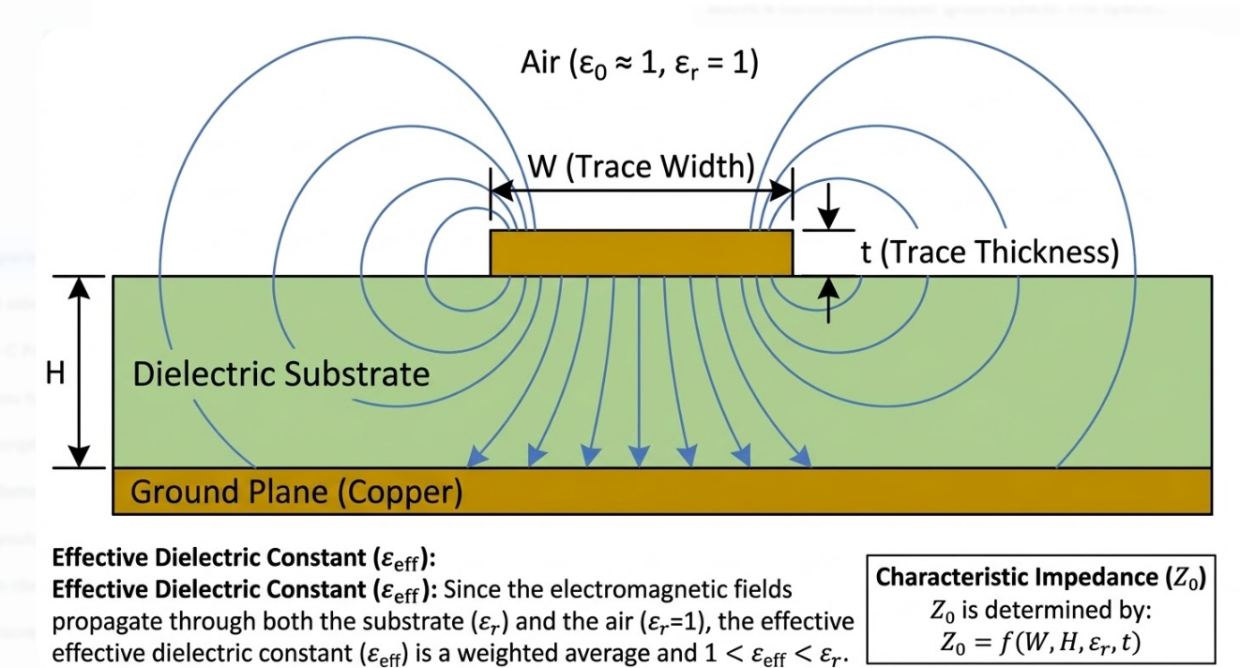
A microstrip line is, therefore, essentially a trace of conductive material on the outer section of PCB, right? This dielectric stuff is what separates it from the following layer with a continuous ground plane. The microstrip is suspended in a mixed dielectric environment, as opposed to a full-boxed structure. The trace takes some of the EM field through the substrate under the trace, and the remainder of it takes a flight through the air or whatever has been coated on top. It is this ambiance that makes the microstrip so special - and it is what makes it so convenient and, at the same time, so difficult.
The important parameters that characterize its electrical behavior are:
- Characteristic impedance (Z0): So when we refer to Z0 on the board, it all boils down to a couple of factors, the trace width, the dielectric height, dielectric constant, and copper thickness. We target in most courses and projects a single-ended 50 ohm or differential pairs at about 90 ohm or 100 ohm, as the textbook says.
- Effective dielectric constant (Dk eff): The effective Dk is a weighted average of substrate Dk and air (air has Dk = 1), it is always slightly less than the raw substrate Dk. In a typical FR4 board, with a Dk of about 4.2-4.5, the effective Dk of the microstrip is about 3.0-3.5.
- Propagation delay: Approximately 5.3-6.0 ps/mm for microstrip on FR4, faster than stripline because of the lower effective Dk.
- Attenuation: The total loss per unit length, which increases with frequency.
Microstrip vs Stripline: Key Differences and Selection Criteria
One of the first and most significant choices you have to make when you are configuring a high-speed PCB stack-up is whether to use microstrip or stripline. In essence, both are controlled-impedance transmission lines; however, they are constructed differently, and they act completely differently.
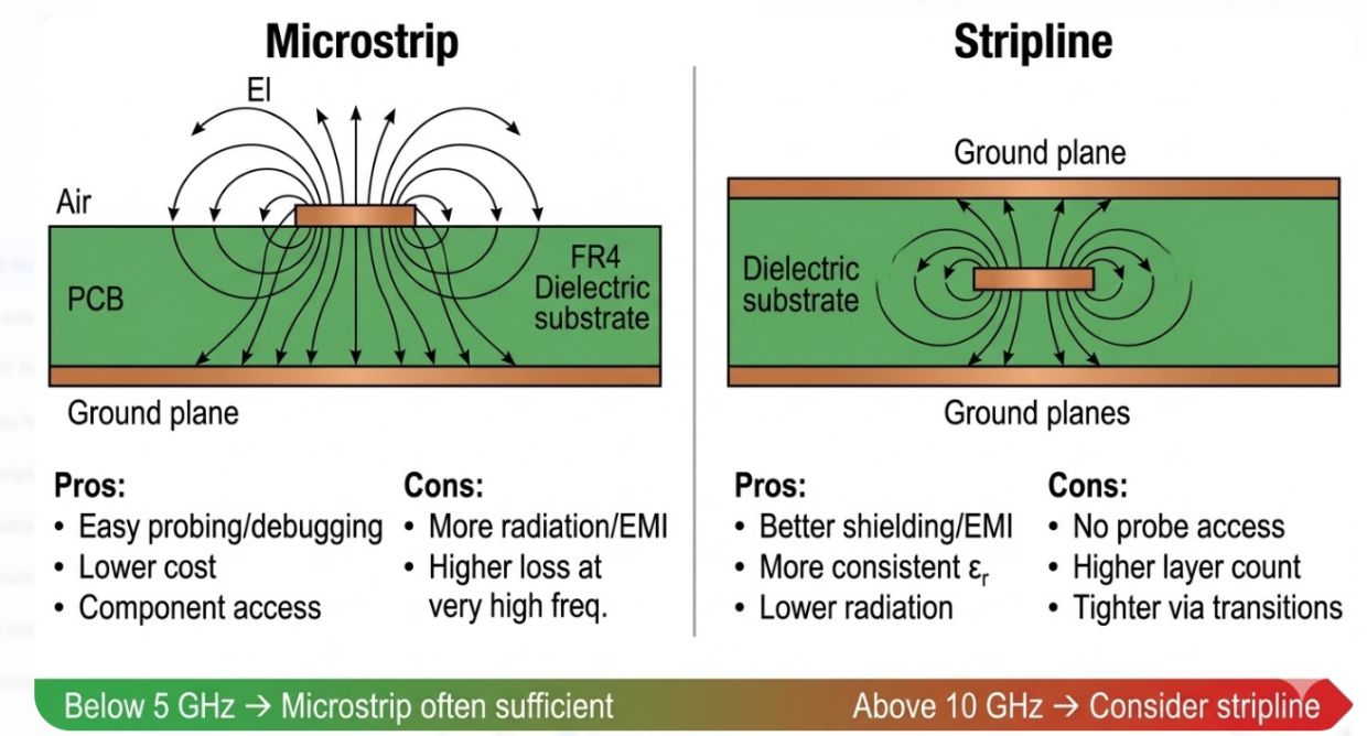
| Parameter | Microstrip | Stripline |
| Location | External layer (top or bottom) | Internal layer (buried between planes) |
| Dielectric environment | Mixed (air + substrate) | Homogeneous (fully enclosed in substrate) |
| EMI radiation | Higher (exposed to air) | Lower (shielded by ground planes) |
| Shielding | Requires additional measures | Inherently shielded |
| Propagation delay | ~5.3-6.0 ps/mm (FR4) | ~6.5-7.0 ps/mm (FR4) |
| Insertion loss | Moderate | Slightly lower at the same Dk/Df |
| Routing accessibility | Easy (outer layer probing, rework) | Difficult (buried, no direct access) |
| Component connection | Direct (surface mount pads) | Requires vias to reach the surface |
| Typical use case | RF circuits, debug-friendly signals, moderate frequency | High-speed digital buses, noise-sensitive signals, dense designs |
With frequencies below 5-6 GHz, we tend more towards microstrip since it is very convenient to trace, simple to test, and it plugs directly into SMDs. However, above 10 GHz, microstrip becomes unattractive, radiation loss peaks, and it becomes sensitive to environmental factors. The critical signals are then most of us shoved into buried striplines since the uniform dielectric is more predictable.
Critical Design Parameters for Microstrip Lines
Impedance Calculation and Line Width Determination
The characteristic impedance of a microstrip line depends on four primary geometric and material parameters:
- Trace width (W): Wider traces have lower impedance. This is the primary variable designers adjust.
- Dielectric height (H): The distance between the trace and the reference plane. A thinner dielectric requires a narrower trace for the same impedance.
- Dielectric constant (Dk): A higher Dk reduces impedance for a given geometry. FR4 typically ranges from 4.2 to 4.7, depending on resin content and frequency.
- Copper thickness (T): Thicker copper slightly reduces impedance by effectively widening the conductive cross-section.
Effective Dielectric Constant and Loss Tangent Considerations
The effective dielectric constant of a microstrip line is always between the Dk of the substrate and 1 (air) effectively. With a typical FR4 board (Dk approximately 4.4) the effective Dk will tend to appear at frequencies in the range of 3.2-3.5, depending on the width of the trace relative to dielectric height. A broader trace than the dielectric height causes more of the electric field to lie within the substrate, which shifts the effective Dk nearer to the full substrate value. With a narrow trace, much of the field spills out into the air, and hence the effective Dk tends to decrease towards the air value.
This is in fact, important in two ways. To begin with, propagation delay is dependent on the effective Dk, when we are length-matching differential pairs or parallel buses, we must use the effective Dk, rather than the effective substrate Dk. Second, the effective Dk is dependent on frequency. The frequency increases, the field narrows in the substrate, the effective Dk increases slightly, and the propagation velocity decreases. Such dispersion can contribute to inter-symbol interference in very high-speed digital connections.
The loss material above approximately 1-2GHz is dominated by dielectric loss, which is caused by the loss tangent (Df) of the material. The dielectric loss of the insertion is proportional to frequency and the Df. In addition, the roughness of copper contributes to the loss since this essentially increases the length of the current path on the conductor surface.
Here is a practical material selection guide based on frequency:
| Frequency Range | Recommended Material | Typical Dk | Typical Df | Notes |
| Below 1 GHz | Standard FR4 | 4.2-4.7 | 0.017-0.025 | Cost-effective, widely available |
| 1-6 GHz | Mid-grade FR4 / Megtron 4 | 3.8-4.4 | 0.008-0.015 | Better loss control, moderate cost |
| 6-15 GHz | Rogers RO4003C / RO4350B | 3.38-3.48 | 0.0027-0.0037 | Low loss, stable Dk, processable on FR4 lines |
| Above 15 GHz | Rogers RT/duroid 5880 / PTFE | 2.2-2.5 | 0.0009-0.002 | Ultra-low loss, specialized processing |
Practical Design Techniques for Reliable Microstrip Performance
Routing Guidelines, Bend Optimization, and Ground Plane Strategies
Getting the cross-section right is only half the battle. How you route the microstrip across the board is equally critical. Here are the essential routing rules for maintaining signal integrity:
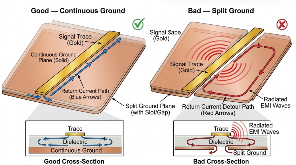
- Maintain a continuous reference plane: The ground plane beneath your microstrip must be unbroken along the entire signal path. Any slot, split, or void in the reference plane forces the return current to detour, creating a loop antenna that radiates and picks up noise.
- Use controlled bends: Right-angle (90-degree) bends create a localized impedance discontinuity because the effective trace width increases at the corner. This causes reflections that become significant above 1-2 GHz.
- Avoid unnecessary neck-downs: Transitioning from a wider trace to a narrower one and back creates impedance bumps. If you must neck down for a BGA escape or tight routing channel, keep the narrow section as short as possible.
- Maintain consistent trace width: Any width variation along the route changes impedance. Use your EDA tool's controlled-impedance routing mode to lock the trace width.
Via Placement and Crosstalk Mitigation
Therefore, in the case that a microstrip signal passes through a via, the return current must switch layers as well. When there is no closed return path, it causes the returning current to make a diversion, in that a loop of current is formed, and the current radiates and distorts the signal quality. The solution is simple: either add a ground via at least right, always adjacent to every signal via, within 20 -30 mils (0.5-0.75 mm).
Another big deal is via stubs, particularly with high frequency. When a signal via passes through the entire board, but only connects two layers, the remaining portion of the barrel is an open stub. The stub forms a quarter-wave notch in the resonance. On a 62-mil (1.6mm) board with a stub of approximately 50mils long, the first resonance appears at about 15-18GHz. Beyond 10Gbps (or 25G Ethernet), back-drilling or blind/buried vias to eliminate those stubs is required. Interfering with neighboring lines of microstrip is dependent on distance, length of coupling, and dielectric geometry. The guidelines in practice are:
- Maintain a minimum 3W spacing (three times the trace width, measured center-to-center) between unrelated signals. This typically reduces crosstalk to below -40 dB.
- Use ground fencing: For highly sensitive signals, route a grounded guard trace between aggressor and victim lines, with ground vias every quarter-wavelength along the guard trace.
- Minimize parallel run length: Crosstalk accumulates over the coupled length. Stagger routes or change layers to reduce parallel exposure.
- Differential routing: Tightly coupled differential pairs inherently reject common-mode noise, including crosstalk from nearby aggressors.
Manufacturing Considerations for High-Frequency Microstrip Lines
Etching Accuracy, Copper Profile Control, and Surface Finish Selection
Thus, our simulation is that of a perfectly rectangular trace cross-section, whereas in the actual factory floor, you have a trapezoidal shape due to chemical etching. The trace will have a larger width at the bottom side where the copper and dielectric meet, and a smaller width at the top. This undercut etch really decreases the effective width and forces the impedance even higher. The etch tolerance typically is approximately ±0.5-1.0 mil when it is standard 1 oz (35 um) copper on the outer layers. Half-ounce copper gives a cleaner profile and tighter tolerances, and that is the reason why many high-speed schemes have ended up with 0.5 oz of copper on the signal layers. Above 2oz and further on, they take even more pronounced trapezoidal shapes, and the impedance is more difficult to predict.
Another source of loss that is easily overlooked by people is copper roughness. FR4 boards use a standard electrodeposited copper foil, which has a surface roughness (Rz) of approximately 5-10 um. The copper skin depth at a frequency above 3-5 GHz falls below 1-2 mm, so that at present the current is flowing in a portion of the circuit that is strongly affected by the texture on the surface. A smooth-surface approximation of the conductor loss can actually increase by 10-30% when using rougher copper.
Surface finish selection also affects high-frequency performance:
| Surface Finish | RF/High-Speed Impact | Assembly Compatibility | Cost |
| ENIG (Electroless Nickel Immersion Gold) | Nickel layer adds loss above 5 GHz (~0.5-1 dB/inch extra) | Excellent for fine-pitch | Moderate |
| OSP (Organic Solderability Preservative) | Minimal additional loss | Good, limited shelf life | Low |
| Immersion Silver | Very low additional loss | Good, tarnish sensitive | Moderate |
| Immersion Tin | Low additional loss | Good, limited reflow cycles | Low-Moderate |
| HASL (Hot Air Solder Leveling) | Surface planarity issues for fine-pitch; moderate loss | Excellent for standard pitch | Low |
| Hard Gold (Gold Fingers) | Suitable for edge connectors only | N/A for SMT pads | High |
Tight Tolerance Control for Consistent Impedance
Achieving a target impedance on one prototype board is relatively straightforward. Reproducing that impedance consistently across hundreds or thousands of boards, lot after lot, requires disciplined process control. The key manufacturing controls include:
- Fixed stackup definition: Lock the stackup with the fabricator. Specify exact prepreg types (e.g., 1080, 2116, 7628), resin content, and lamination parameters. Any stackup change, even substituting one prepreg style for another with the same nominal thickness, can shift impedance.
- Impedance test coupons: Include impedance test coupons on the production panel. These are sacrificial traces built with the same geometry as your controlled-impedance nets, measured by TDR (Time Domain Reflectometry) to verify impedance before boards ship.
- Defined tolerance bands: Standard controlled-impedance tolerance is plus or minus 10%. Tighter tolerances of plus or minus 7% or even plus or minus 5% are available from capable fabricators but require more process control and may increase cost.
These controls are captured formally in IPC-6012 Class 2 and Class 3 specifications, which define the qualification and performance requirements for rigid PCBs, including controlled-impedance tolerance.
JLCPCB's Expertise in Delivering High-Speed Microstrip PCBs
Advanced Fabrication for Precise Impedance and Low Loss
In the case of controlled-impedance microstrip PCBs JLCPCB offers this complete impedance control service that can be used with standard and high-frequency designs. Their online impedance calculator is integrated directly into their ordering system, where you can select one of the real production stackups and calculate the impedance of single-endedd microstrip, differential microstrip, single-ended stripline, as well as differential stripline configurations.
Key capability highlights include:
- Impedance tolerance: Standard plus or minus 10%, with tighter tolerances available on request for advanced designs.
- Layer support: Controlled impedance available for 4-layer through 14+ layer stackups.
- Material options: Standard FR4 (Tg150-170 °CC), mid-loss laminates, and Rogers high-frequency materials for demanding RF applications.
- Copper weights: 0.5 oz to 2 oz on signal layers, enabling fine-line routing for impedance-sensitive designs.
Reliable Production from Prototypes to Volume Runs
The largest bane of high-speed PCB construction is ensuring that the boards will act the same when you scale from just a few prototypes (5 -10 boards) onto full-scale runs (hundreds or thousands): In case a board reaches the impedance spec during the prototype stage, it must still nail that spec when you bulk it out.
JLCPCB addresses this through a reproducibility framework built on several pillars:
- Consistent process window: The same etching chemistry, lamination pressures, and plating parameters used for prototypes are applied to production runs. There is no "prototype process" versus "production process" that could shift impedance.
- Same impedance control assumptions: The stackup and impedance calculations established during prototyping are carried forward to volume orders. Changes to laminate suppliers or prepreg types that could affect Dk are managed through a change control process.
- Change control notifications: If a material substitution is necessary (e.g., a specific prepreg style becomes unavailable), JLCPCB communicates the change and its potential impedance impact before proceeding.
- Statistical process control (SPC): Impedance coupon data from production panels is tracked statistically, allowing real-time monitoring of process stability across the entire production lot.
Frequently Asked Questions (FAQ)
Q1: 1. When should I use microstrip instead of stripline for high-speed signals?
Use microstrip when your signals need direct access to surface-mount components, test points, or tuning elements. Microstrip is also preferred for RF circuits where post-fabrication tuning may be needed. Switch to stripline when EMI shielding, crosstalk isolation, or propagation consistency is the priority, particularly for signals above 6-10 GHz or dense digital buses like DDR4/DDR5.
Q2: How do I set the correct target impedance for my microstrip lines?
Your target impedance is determined by the interface standard you are implementing. USB 3.0 specifies 90 ohm differential, PCIe requires 85 ohm differential, and most single-ended RF circuits use 50 ohm. Check the datasheet or interface specification for your specific protocol, then design your stackup and trace width to hit that target.
Q3: What inputs does an impedance calculator need for microstrip calculations?
At minimum, you need: trace width (W), dielectric height (H), dielectric constant (Dk) of the substrate, and copper thickness (T). For a differential microstrip, you also need the trace spacing (S). For best accuracy, use the fabricator's actual stackup data rather than generic laminate values.
Q4: 4. How can I reduce insertion loss in my microstrip lines?
Focus on three areas. First, select a lower-Df laminate material appropriate for your frequency (see the material table above). Second, specify low-profile copper foil to reduce conductor roughness loss. Third, choose a surface finish with minimal RF impact, such as OSP or immersion silver instead of ENIG, if your assembly process allows it.
Q5: Should I use mitered bends or curved bends for microstrip routing?
Below 5 GHz, both perform well, and the difference is negligible. Between 5-15 GHz, a well-executed miter (60-70% corner removal) is usually sufficient. Above 15 GHz, curved bends with a radius of at least 3 times the trace width provide measurably better return loss. If your EDA tool supports arc routing, use it for critical high-frequency paths.
Keep Learning
How Modular PCB Design Simplifies Complex Electronics Projects
Key Takeaway Modular PCB design simplifies complex electronics by breaking boards into independent, reusable functional blocks with clear interfaces. It boosts reusability, speeds up debugging, enhances team collaboration, and reduces errors.Shift from flat to modular design for faster development and more scalable, reliable PCBs. Ever seen a 400+ component schematic and got your head scrambled before even beginning routing? You are not alone. With the ever-increasing density of electronics combined w......
Your Ultimate Guide to PCB Rulers
In the world of PCB design and manufacturing, having the right tools is crucial for achieving accuracy and precision. One such tool that has gained popularity among professionals and hobbyists is the PCB ruler. This specialized measuring tool is designed to provide accurate measurements, reference information, and component footprints, assisting designers, engineers, technicians, and assemblers in various stages of PCB development. In this guide, we'll explore what a PCB ruler is, the features and mea......
Understanding the Materials Used in PCBs: Selection, Types, and Importance
Key Takeaways FR-4 is the go-to material for most cost-effective and reliable PCBs. Use Rogers for high-frequency and RF applications to reduce signal loss. Higher copper weight (2oz) improves current and heat handling. Choose High-Tg substrates for better thermal stability in multilayer boards. Green LPI soldermask offers the best balance of performance and inspection. Printed circuit boards (PCBs) are an essential component of modern electronics. These boards connect and support electronic component......
How to Select Tg of PCB ?
What is the Tg of PCB? In PCB manufacturing, "Tg" stands for Glass Transition Temperature. It is the temperature at which the PCB substrate material transitions from a rigid, glassy state to a soft, rubbery state. PCBs are flame-retardant (UL94 V-0) and do not burn easily; instead, they soften above Tg. The Critical Correlation Between Tg and Z-Axis CTE (Coefficient of Thermal Expansion) When the temperature exceeds the Tg point, the PCB substrate material (such as standard FR-4) undergoes a physical ......
How to Choose the Thickness of PCB
First, In the world of electronic products, the PCB is often referred to as the "heart" of the device. It interconnects all components, making board thickness one of the most important parameters. Choosing the right PCB thickness directly affects the electrical performance, mechanical stability, thermal management, and long-term reliability of the final electronic product. The process of selecting PCB thickness is influenced by various factors, such as product application scenarios, board material, an......
PCB Copper Pour Basics
What is Copper Pour in PCB Design? Copper pour refers to the technique of filling unused areas of a PCB's copper layers with solid copper planes. These planes are connected to power or ground nets, creating a continuous conductive path. Copper pour is typically used in the power and ground planes, as well as in signal layers for specific purposes. Purpose and Benefits of Copper Pour: Copper pour is primarily used to fill unused areas on PCB copper layers with solid (or hatched) copper connected to pow......