Don't Let Design Errors Ruin Your Hardware: The Complete Guide to PCB Design Verification
12 min
- Why PCB Design Verification is Non-Negotiable
- Schematic and Logical Verification
- PCB Layout and Design Rule Checking (DRC)
- Design for Manufacturing (DFM) – The Bridge to Production
- Transforming Verified Designs into Reality: JLCPCB's Advanced Manufacturing Capabilities
- FAQ about PCB Design Verification
- Conclusion on PCB Design Verification
Key Takeaways
- PCB design verification is the systematic process of validating layouts against electrical, signal integrity, and manufacturing rules before production, preventing costly board respins and launch delays.
- Schematic verification through Electrical Rules Check (ERC) catches floating inputs, power shorts, and footprint mismatches before layout begins.
- Design Rule Checking (DRC) ensures trace widths, clearances, and via sizes comply with your fabricator's manufacturing tolerances, especially for controlled-impedance multilayer designs.
- Design for Manufacturing (DFM) analysis catches issues like acid traps, slivers, and solder mask gaps that standard DRC overlooks, optimizing production yields.
- JLCPCB's automated cloud-based DFM platform provides instant design validation and supports up to 32-layer advanced manufacturing with rigorous AOI and flying probe testing.
Why PCB Design Verification is Non-Negotiable
PCB design verification is the comprehensive engineering process of validating a printed circuit board layout against electrical, signal integrity, and manufacturing rules before hardware production. Skipping this crucial phase frequently leads to catastrophic circuit failures, expensive board respins, and missed product launch windows.
The margin for error in modern electronics design has narrowed to micrometer thresholds. As electronic components shrink and signal frequencies ascend into the gigahertz spectrum, a single unverified trace or an overlooked clearance constraint can render an entire production batch completely useless. Hardware engineering teams cannot afford to treat physical prototypes as debugging platforms; instead, validation must happen deterministically within the digital domain.
The financial and operational consequences of engineering re-work—commonly known as a board respin—extend far beyond the baseline price of raw FR4 and copper. When an unverified design moves straight to production, engineering teams lose valuable time diagnosing physical boards under oscilloscopes and thermal cameras, slipping schedules by weeks or months. By implementing a rigorous PCB design verification workflow, engineering departments establish a robust gate that translates virtual CAD models into perfectly functioning, manufacturability-ready hardware.
Schematic and Logical Verification
Schematic and logical verification detects systemic connectivity errors, footprint mismatches, and net list discrepancies before the physical board layout begins. Resolving these electrical anomalies at the logical level prevents fundamental schematic errors from propagating into the copper layout.
Electrical Rules Check (ERC): Catching Disconnected Pins and Power Shorts
Before a single trace is routed, the Electrical Rules Check (ERC) serves as the primary defense against logical errors. This automated verification process evaluates the schematic netlist against predefined matrix rules to isolate floating inputs, conflicting pin types, and missing power connections.
A properly configured ERC matrix immediately highlights severe design flaws, such as driving a single net with two active output pins or leaving high-impedance inputs entirely unterminated. Catching these logical oversights prevents power-to-ground dead shorts that could permanently damage components during the initial bench power-up.
Component Footprint Verification: Matching Schematic Symbols to Real-World Land Patterns
Component footprint verification confirms that the virtual 2D land patterns inside your CAD library correspond perfectly with the physical dimensions and pitch of actual surface-mount (SMD) and through-hole (PTH) components. This step eliminates discrepancies between the mechanical data sheets provided by vendors and the actual geometric layout on the board.
Engineers must manually cross-verify pin-number ordering—particularly on polarized components like diodes, electrolytic capacitors, and complex discrete transistors (e.g., SOT-23 packages)—against manufacturer datasheets. A mismatch between a schematic symbol pinout and the corresponding physical footprint footprint leads to misplaced copper pads, making manual rework difficult or rendering the board completely unsolderable during assembly.
Simulation and Signal Integrity (SI) Pre-Layout Checks
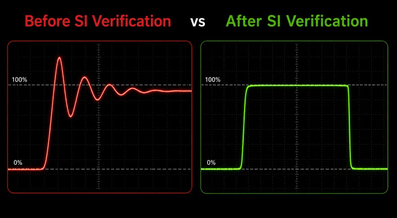
Pre-layout signal integrity (SI) simulation models the electrical behavior of critical networks, such as high-speed data buses and clocks, prior to physical routing. This predictive analysis allows designers to define terminal impedance constraints, evaluate transmission line topologies, and mitigate potential reflections.
By running SPICE or behavioral IBIS simulations at the schematic stage, hardware engineers can determine the exact series termination resistor values required to match source impedances. This proactive verification guarantees that high-speed signal transitions retain clean, stable edges, eliminating problematic ringing and overshoot before any physical traces are drawn.
PCB Layout and Design Rule Checking (DRC)
Design Rule Checking (DRC) validates physical layout geometry against the specific manufacturing limits of your fabrication partner to guarantee signal integrity and structural reliability. Properly configured constraints ensure that line widths, spacing, and via structures comply fully with precision manufacturing tolerances.
Setting Up Constraints: Trace Widths, Clearances, and Via Sizes
Configuring the Design Rule Check (DRC) engine inside your EDA tool requires translating your fabricator's precise mechanical capabilities into strict software constraints. These parameters define minimum allowable trace widths, edge-to-edge clearances, and drill-to-copper limits across different layers.
Adhering strictly to these manufacturing limits prevents catastrophic over-etching, which can cause narrow traces to narrow excessively or break completely. Maintaining conservative spacing margins significantly minimizes the risk of copper bridges forming during the chemical etching process.
| Parameter | JLCPCB Standard Minimum Spec (1 oz Copper) | Recommended Design Target (For Optimal Yield) |
|---|---|---|
| Minimum Trace Width | 3.5 mil (0.09mm) for Multilayer | 5.0 to 6.0 mil |
| Minimum Trace Spacing | 3.5 mil (0.09mm) for Multilayer | 5.0 to 6.0 mil |
| Minimum Via Drill Diameter | 0.2 mm (8 mil) | 0.3 mm |
| Minimum Via Pad Diameter | 0.45 mm (18 mil) | 0.6 mm |
| Via-to-Via Clearance | 5.0 mil (0.127mm) for 4L+ | 10.0 mil |
Advanced DRC for Multilayer PCBs: Controlled Impedance and Layer Stackup
For multi-layer architectures handling high-speed signaling (such as PCIe, USB 3.0, or DDR memory), the DRC must validate the precise geometric parameters required for controlled impedance. Trace widths and reference plane clearances must adapt dynamically based on the specific dielectric constant (e_r) and layer stackup heights of the manufacturing core and prepreg materials.
When routing differential pairs, the DRC engine continuously monitors trace widths, intra-pair spacing, and length matching tolerances. Ensuring that high-speed traces maintain a uniform cross-section prevents sudden changes in characteristic impedance, eliminating signal reflections and maintaining compliance with strict electromagnetic compatibility (EMC) standards.

Thermal Management Verification: Thermal Vias and Dissipation Paths
Thermal management verification ensures that high-power components, such as switching regulators, MOSFETs, and processors, have clear paths to dissipate heat. The physical layout must provide sufficient thermal vias, solid copper planes, and adequate spacing around heat sinks.
Layout engineers must verify that power pads contain an optimized array of thermal vias linked directly to inner ground planes acting as heat sinks. Additionally, the DRC should confirm that components intended for automated wave or reflow soldering utilize proper thermal relief connections. This balances heat distribution during assembly and prevents tombstoning or cold solder joints caused by excessive heat sinking during production.
Design for Manufacturing (DFM) – The Bridge to Production
Design for Manufacturing (DFM) bridges the gap between layout geometry and real-world factory production by identifying physical defects that clear standard CAD rule checks but cause assembly issues. Resolving these challenges significantly optimizes manufacturing yields, reduces lead times, and lowers overall production costs.
What is DFM and Why Fabricators Care?
While a standard DRC confirms that a layout adheres to baseline electrical constraints, a Design for Manufacturing (DFM) check analyzes whether the board can be reliably fabricated and assembled on automated production lines. DFM bridges the gap between theoretical CAD models and the practical realities of chemical etching, mechanical drilling, and reflow soldering.
Fabricators prioritize DFM because layout anomalies directly affect fabrication yields and line efficiency. A design optimized for DFM moves smoothly through production without requiring manual interventions, engineering queries (EQs), or costly line stoppages, lowering manufacturing costs for both the customer and the factory.
Common DFM Issues that Delay Production
Several common DFM oversights frequently clear standard EDA software checks but cause significant problems on the factory floor:
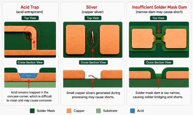
- Acid Traps: Traces meeting at acute angles (<90°) can trap residual etching chemicals, leading to over-etched copper and localized open circuits.
- Slivers: Narrow, isolated wedges of copper or solder mask can peel off during fabrication, floating across the board and creating intermittent electrical shorts.
- Insufficient Solder Mask Dams: When the solder mask bridge between adjacent SMD pads is too narrow, molten solder can bridge during reflow, causing component shorts.
Generating Flawless Production Files: Gerber RS-274X/X2 and ODB++
The final step in the design verification process is exporting your layout into standard manufacturing file formats like Gerber RS-274X, Gerber X2, or ODB++. Errors during file generation can corrupt layer stackups, misalign drill holes, or omit critical copper structures entirely.
Before submitting any files to production, designers must verify the exported data using an independent, third-party Gerber viewer. This extra step confirms that custom pad shapes, slot drill details, and outline profiles render correctly, preventing translation issues between your CAD software and the factory's CAM automated equipment.
Transforming Verified Designs into Reality: JLCPCB's Advanced Manufacturing Capabilities
JLCPCB transforms verified digital layouts into high-reliability hardware by combining a fully automated cloud-based DFM platform with advanced multi-layer manufacturing processes. Their integration of real-time design validation and high-precision fabrication ensures industrial-grade quality for complex, high-density designs.

Automated DFM Cloud Check: How JLCPCB Screens Your Files Instantly
JLCPCB automates the verification pipeline with their advanced JLCDFM platform, a free, intelligent online analysis tool that instantly validates manufacturing files. The moment a designer uploads a Gerber package, the platform scans the geometry against real-world production tolerances, identifying potential errors before any order is finalized.
The system performs automated checks across five core modules: copper traces, solder masks, drilling layers, silkscreens, and component assembly. Any design anomalies—such as insufficient solder mask dams or drill-to-copper violations—are instantly flagged in a visual report, allowing engineers to correct layout errors before production begins.
Precision Engineering for Complex Designs: Multi-Layer PCBs and Microvias
For complex, high-density designs, JLCPCB provides industrial-grade manufacturing capabilities supporting architectures up to 32 layers. This advanced fabrication handles tight trace spacing, controlled impedance routing, and microvia structures with excellent mechanical repeatability.
By utilizing high-accuracy Laser Direct Imaging (LDI) and modern vertical plating lines, JLCPCB ensures excellent trace uniformity and layer-to-layer alignment. This tight tolerance control is essential for maintaining predictable signal integrity across high-speed differential pairs and fine-pitch BGA breakouts.
Industry-Leading Quality Control: From AOI to Flying Probe Testing
To ensure every board matches the verified design files, JLCPCB integrates rigorous quality control checkpoints throughout the manufacturing line. Automated Optical Inspection (AOI) scanning systems inspect every layer post-etching, comparing the physical copper against the original Gerber data to catch micro-shorts or hairline cracks.
Following fabrication, boards undergo automated Flying Probe testing or dedicated bed-of-nails electrical checks to confirm 100% netlist continuity. These comprehensive test procedures ensure that hidden internal layer vias and micro-vias are completely free of open circuits or high-resistance defects before the boards ship.
High-Grade Materials and Certifications
JLCPCB maintains exceptional product reliability by sourcing premium raw materials and adhering to international manufacturing standards. Production lines utilize trusted, industry-standard laminates (including high-Tg FR4, aluminum cores, and specialized Rogers RF dielectrics) to ensure thermal stability under demanding operational conditions.
All manufacturing facilities operate under strict ISO9001 quality management systems and maintain full RoHS compliance. This commitment to standardized, certified production guarantees that prototype runs translate seamlessly into high-yield, long-term commercial production.
FAQ about PCB Design Verification
Q: What is PCB design verification?
PCB design verification is the engineering process of validating a printed circuit board layout against electrical, signal integrity, and manufacturing rules before sending it to production. It includes schematic checks (ERC), layout checks (DRC), and manufacturability analysis (DFM) to prevent costly board failures and respins.
Q: What is the difference between DRC and DFM?
DRC (Design Rule Checking) validates that your layout meets baseline electrical and geometric constraints like trace width and spacing. DFM (Design for Manufacturing) goes further by analyzing whether the board can be reliably fabricated and assembled on real production lines, catching issues like acid traps, slivers, and solder mask problems that DRC overlooks.
Q: Why is schematic verification important before layout?
Schematic verification through Electrical Rules Check (ERC) catches fundamental connectivity errors—like floating inputs, shorted power nets, and footprint mismatches—before a single trace is routed. Fixing these issues at the logical level is far easier and cheaper than discovering them on a physical prototype.
Q: What manufacturing file formats should I use for PCB production?
Industry-standard formats include Gerber RS-274X, Gerber X2, and ODB++. Always verify your exported files using an independent Gerber viewer before submission to ensure layers, drill holes, and outlines render correctly and match your design intent.
Q: How does JLCPCB help with design verification?
JLCPCB offers the free JLCDFM platform that automatically scans your uploaded Gerber files against real-world manufacturing tolerances. It checks copper traces, solder masks, drilling layers, silkscreens, and component assembly, flagging potential issues in an instant visual report so you can correct errors before production begins.
Conclusion on PCB Design Verification
Executing a thorough PCB design verification workflow is the single most effective strategy for mitigating the risks, expenses, and delays associated with hardware development. By systematically validating your schematics, refining layout design rules, and performing comprehensive DFM analysis, you transform your design from a conceptual blueprint into an optimized file package ready for seamless, high-yield manufacturing.
When you partner with JLCPCB, you gain access to more than just a standard manufacturing facility; you leverage a highly integrated hardware ecosystem engineered to eliminate production errors. From the instant cloud-based DFM analysis tool that checks your files on upload, to advanced multi-layer automated fabrication lines and rigorous AOI/flying-probe testing, JLCPCB ensures your designs are built to the highest industry standards. Bring your next hardware project to life with precision and efficiency—upload your verified Gerber files to JLCPCB today and experience professional-grade manufacturing.
Popular Articles
• AI PCB Design: From Prompt to PCB with EasyEDA Pro
• AI Tools for PCB Design: Which Tool Fits Your Workflow Stage?
• GPT-6 Astra PCB Design in KiCad: From Brief to Verified Native Project
• GPT-6 Astra PCB Design in EasyEDA Pro: What Worked, What Failed, and What We Learned
• How to Design Your Own Keyboard PCB: From Layout to Firmware
Keep Learning
AI Tools for PCB Design: Which Tool Fits Your Workflow Stage?
AI tools can now assist with PCB architecture, schematic generation, component selection, placement, routing, and design verification. However, different tools target different stages of the PCB workflow. This guide compares AI tools for PCB design based on what they actually do, what inputs they require, and where they fit within a real engineering workflow. In this guide, you will learn: The 6 types of AI PCB tools and the input each one needs What AI PCB design tools do, compared stage by stage How......
Free Online Circuit Simulator for Electronics Engineers
Key Takeaways Simulate First: Free circuit simulators prevent fried components and cut PCB re-spins. Fix AC Sweep: Enter pure numbers for points per decade, not time units. Use SMD Parts: Swap ideal models for standard SMD resistors and SOT-23 transistors. Control Parasitics: Board trace capacitance and via inductance alter high-frequency signals. Verify Before Order: Pair SPICE simulation with DFM checks to ensure board success. If all electronic engineers had a dollar for each burnt-out resistor or ......
Mastering PCB Design Rules: A Comprehensive Guide for Optimal Results
Key Takeaways Follow core PCB design rules for reliable electrical and mechanical performance. Optimize trace width, spacing, impedance, and vias for signal integrity and manufacturability. Apply DFM and DRC early to identify potential manufacturing and layout issues. Consider thermal management, grounding, and testing during the PCB design stage. Align design rules with your PCB manufacturer’s capabilities to improve production reliability and reduce redesigns. PCB design rules are essential guidelin......
KiCad MCP: How to Design a PCB with Claude Code [Step-by-Step]
Key Takeaways Claude can design PCBs in KiCad: By connecting Claude to KiCad through an MCP server, you can use AI to create and modify PCB designs. In this project, Claude helped turn a 5 A XL4015 buck converter netlist into a two-layer, 63 × 33 mm PCB layout with zero ERC violations and zero DRC errors after minor initial fixes. Set up Claude securely: Use a KiCad MCP server that starts in read-only mode. Review the server code before installing it, connect through stdio, and allow editing only in a......
Claude Code PCB Design: Can It Build a Real Board in EasyEDA Pro?
Key Takeaways Claude Code PCB design: Using Claude Opus 5.5 and EasyEDA Pro 3.2.149, I converted a 47-component, three-page schematic from a PDF into a fully routed, two-layer PCB with zero DRC errors. EasyEDA Pro integration: The EasyEDA API skill connects Claude Code to EasyEDA Pro through a local bridge server and the Run API Gateway extension. This allows Claude to control the editor via JavaScript, with a 30-second timeout per API call. Design verification: A successful API response doesn't alway......
How to Design a PCB with Flux.ai (Step-by-Step Guide)
Key Takeaways This step-by-step Flux PCB design tutorial demonstrates the complete workflow by creating a compact 15 × 15 mm USB 2.0 hub, refining the layout, routing high-speed differential traces, and preparing manufacturing files for JLCPCB PCB fabrication and assembly. We are all hearing news; new AI models are being released every month. And it has finally reached the schematic editor. Flux.ai is a browser-based AI PCB design tool with a built-in AI agent that behaves like a junior hardware engin......