Mixed Technology PCB Assembly: Combining SMT and THT on One Board
19 min
- What "Mixed PCB Assembly" Actually Means
- The Mixed Assembly Process: Sequencing SMT and THT on One Board
- Stencil Setup for Mixed PCB Assembly
- Design Rules for a Mixed PCB Assembly Board
- Common Challenges in Mixed PCB Assembly
- FAQ about Mixed PCB Assembly
- Conclusion: Treating Mixed PCB Assembly as a System, Not a Step
As technologies become increasingly more complex, the demand for sophisticated printed circuit boards continues to rise. In the electronics industry, the two most prevalent PCB Assembly technologies are SMT and THT, which differ mainly in the manner at which the components are attached. SMT places the components on the surface of the board whereas THT makes use of drilled holes to solder components.
While these technologies individually cater to specific applications, advancements in the electronics industry have made mixed PCB assembly possible. At its core, hybrid PCB assembly combines SMT and through hole on same board, taking advantage of the best of both worlds.
As straightforward as it sounds, the mixed assembly process is a sequenced manufacturing flow that requires precision and accuracy. Contrary to popular first impressions, hybrid PCB assembly is not merely an SMT board with a few through-hole parts added. Errors in the assembly sequence could greatly reduce the manufacturing yield.
Key Takeaways
Integrated SMT + THT: Mixed PCB assembly allows the seamless integration of Surface Mount Technology (SMT) and Through-Hole Technology (THT) on a single board.
Why mixed assembly: Mixed technology PCB assembly is highly beneficial for applications that require the high density of SMT and the extreme mechanical strength of THT.
Standard sequence: Standard hybrid PCB assembly follows a multi-step sequence, involving the reflow process for the SMT side, THT components insertion, and a final wave or selective soldering for the through-hole joints.
Pin-in-Paste option: Alternatively, a second option for mixed technology PCB assembly involves Pin-in-Paste (PIP), which allows THT parts to be reflowed alongside SMT through paste-filled holes, eliminating the final wave step present in standard workflows.
Two stencil setup: For mixed boards, it is recommended to use a precision paste stencil for the SMT side and a red-glue stencil for bottom-side SMD facing the wave.
Industry default: Most production boards beyond hobby grade employ mixed PCB assembly, requiring careful sequencing and the right equipment.
What "Mixed PCB Assembly" Actually Means
In the context of industrial electronics manufacturing, Mixed PCB Assembly, also sometimes referred to as mixed technology PCB assembly, hybrid PCB assembly, or mixed-tech assembly, incorporates both SMT and THT components. A single PCB manufactured using mixed-tech assembly is populated with both surface-mount and through-hole components on a single board, often utilizing a sequenced manufacturing flow rather than a single process.
It is important to note that mixed PCB assembly largely differs from pure SMT or THT workflows as individual SMT decisions can affect THT outcomes and vice versa. As such, having a balanced mindset in SMT and THT design is critical to ensure a successful wave step within the manufacturing line.
When You Need Mixed Assembly
Aside from knowing what mixed technology PCB assembly actually means, it is also just as important to know when you need mixed assembly. Some of the most common scenarios in which mixed assembly process becomes a necessity are as follows:
- Some of the connectors for the components require high mechanical strength, for instance, USB, RJ45, DIN, or board-to-board. For such components, combining SMT parts with through-hole components maximizes performance while maintaining insertion integrity.
- Large electrolytics, transformers, or screw terminals are present, which generally benefit from large through-hole lead areas to handle high-current density during operation.
- High-power dissipation components such as TO-220 regulators and large heatsinks are used, which efficiently conduct heat into copper plates via through-hole leads.
- Components like relays, HV devices, and panel mounts are expected to experience heavy and frequent mechanical stresses but can withstand shock and vibration when effective through-hole joints are established.
- Advanced circuit boards containing mixed-signal blocks with fine-pitch SMT ICs sometimes only have legacy analog parts sold in through-hole packages.
- If none of the previous cases apply, going pure SMT, sometimes via Pin-in-Paste for the remaining components utilizing THT form factors, can usually simplify the manufacturing process.
How Mixed Assembly Differs from Pure-SMT or Pure-THT
| Aspect | Pure SMT | Pure THT | Mixed Technology |
|---|---|---|---|
| Components | Uses surface mount devices (SMD) | Uses leaded components | Combines SMDs with through-hole components on same board |
| Core Processes | Solder paste printing, component placement, reflow soldering | Through hole component insertion, followed by wave, selective, or hand soldering | SMT reflow, THT insertion, wave or selective soldering |
| Joint strength | Low: relies on effective intermetallic compound formation | High: lead through-holes exhibit high mechanical strength | Variable: THT components and SMT parts can lead to variable joint strengths |
| Density/size range | Extremely dense as SMDs are very compact | Larger THT components lead to lower density | Balanced density as a result of the combination of SMD and THT components |
| Main cost driver | Paste printing | Equipment | Manufacturing toolchains, stencils |
| Typical use | High-throughput devices such as consumer electronics | Assemblies requiring hefty parts that need to withstand frequent or high mechanical stresses | Most modern boards |
Although pure SMT and THT cater to specific applications, most production PCBs above hobby grade are mixed by default. As such, the question for most professional grade boards is not whether to use mixed assembly but how to sequence the workflow and prepare the right equipment for it.
The Mixed Assembly Process: Sequencing SMT and THT on One Board
The successful implementation of mixed assembly process relies heavily on the correct sequencing of workflows. In hybrid PCB assembly, the order matters. Every step exposes the previous step’s joints to thermal stress, thereby requiring the proper order to preserve yield. Currently, there are two industry-standard sequences for mixed assembly process.
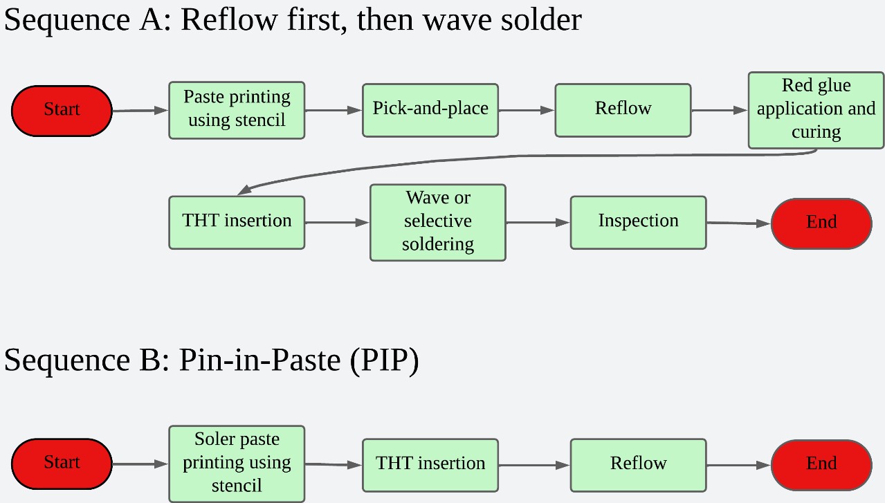
The first one, hereafter referred to as sequence A, implements reflow and wave soldering chronologically. The second industry-standard sequence, hereafter referred to as sequence B, takes advantage of Pin-in-Paste to effectively subject the board in one reflow pass.
Sequence A: Reflow First, Then Wave Solder
- Using a precision stencil, paste print on the SMT side. The quality of the stencil drives the yield. Issues such as bridging, deposit insufficiency, and tombstoning can arise from poor quality stencils.
- Pick-and-place process commences to position the SMT components.
- After successful SMT placement, reflow process is implemented to solder the parts.
- The board is then flipped and red glue is applied on the bottom surface so that the SMD faces the wave. The red glue stencil deposits the adhesive dots.
- After the glue is applied, the bottom-side SMD is placed and the board undergoes glue cure via thermal or UV application.
- The THT components are then inserted from the top-side.
- Depending on the equipment available or the application, wave or selective soldering may be done to solder the THT leads and the glued bottom-side SMD. In this step, selective soldering may be done when only a few THT joints exist.
- Finally, thorough inspection is facilitated along with the required electrical, AOI, X-ray (BGAs) and in-circuit tests.
Sequence B: Pin-in-Paste (PIP) —Mixing in One Reflow Pass
An alternate mixed assembly sequence utilizes Pin-in-Paste that effectively involves only one reflow pass to solder both the SMD and THT components. The process starts by printing PIP paste into the through-hole barrels alongside the SMT pads on the same stencil. The THT parts are then inserted before the reflow process. In this case, both SMT and THT joints form in one reflow pass, eliminating the need for an isolated wave soldering step.
Since the wave solder step is removed in sequence B, the equipment cost is reduced and the flow is shortened by 1 to 2 steps compared to sequence A. However, the caveat with PIP is that it only works for low-to-medium pin THT count (connectors less than 20 pins with smaller caps), frequently failing on large, high-thermal-mass components that prevent the solder paste within the hole from reaching the required reflow temperature. Furthermore, PIP requires more complex stencil design, following enlarged apertures over the barrels to deposit enough paste to fill the hole. Since the extra paste volume is the tradeoff that makes PIP work, it renders some THT parts incompatible.
Choosing the Right Sequence for Your Board
| Factor | Sequence A (Reflow→Wave/Selective) | Sequence B (Pin-in-Paste) |
|---|---|---|
| Best for | Mixed boards with top-side and bottom-side components | Streamlining mixed assembly process by forming THT and SMT joints in one reflow pass |
| THT part types | All standard THT parts | Low-to-medium THT pin counts and smaller capacitors |
| Extra equipment | Wave or selective soldering machines, red-glue stencil, thermal/UV glue curing equipment | None |
| Process steps | Features an eight-step workflow, involving paste printing, reflow, glue application, glue curing, and soldering | Paste printing, THT insertion, and reflow |
| Stencil complexity | Standard precision stencil for solder pastes and red-glue stencil for adhesive dots | Higher stencil design complexity with larger aperture requirements for large paste volume filling |
| When to avoid | Reduce equipment cost or shorten production flow | Applications with large heat-mass parts or incompatible THT components |
Stencil Setup for Mixed PCB Assembly
As mixed boards cater for both SMT and THT components, it is common to utilize more than one stencil. When designing mixed PCB technologies, it is vital to consider upfront costs including stencil requirements so as to avoid late-stage surprises.
The Solder Paste Stencil (the foundation)
Everything starts with the solder paste stencil. As previously mentioned, a poor-quality stencil can impact the production yield. Standard fine-pitch SMT stencils typically feature a foil thickness of 0.10 – 0.15 mm, determined by the smallest component pitch. For mixed technology PCB assembly, the aperture rules remain consistent with pure-SMT based on IPC-7525C (2021): area ratio ≥0.66, aspect ratio ≥1.5.
For hybrid PCB expected to undergo wave after reflow, electropolished apertures and nano-coated foils are recommended to reduce paste smears across long runs. For mixed boards that combine 0.4 mm-pitch BGAs with TO-220 thermal pads, step stencils can be used to vary thickness by zone.
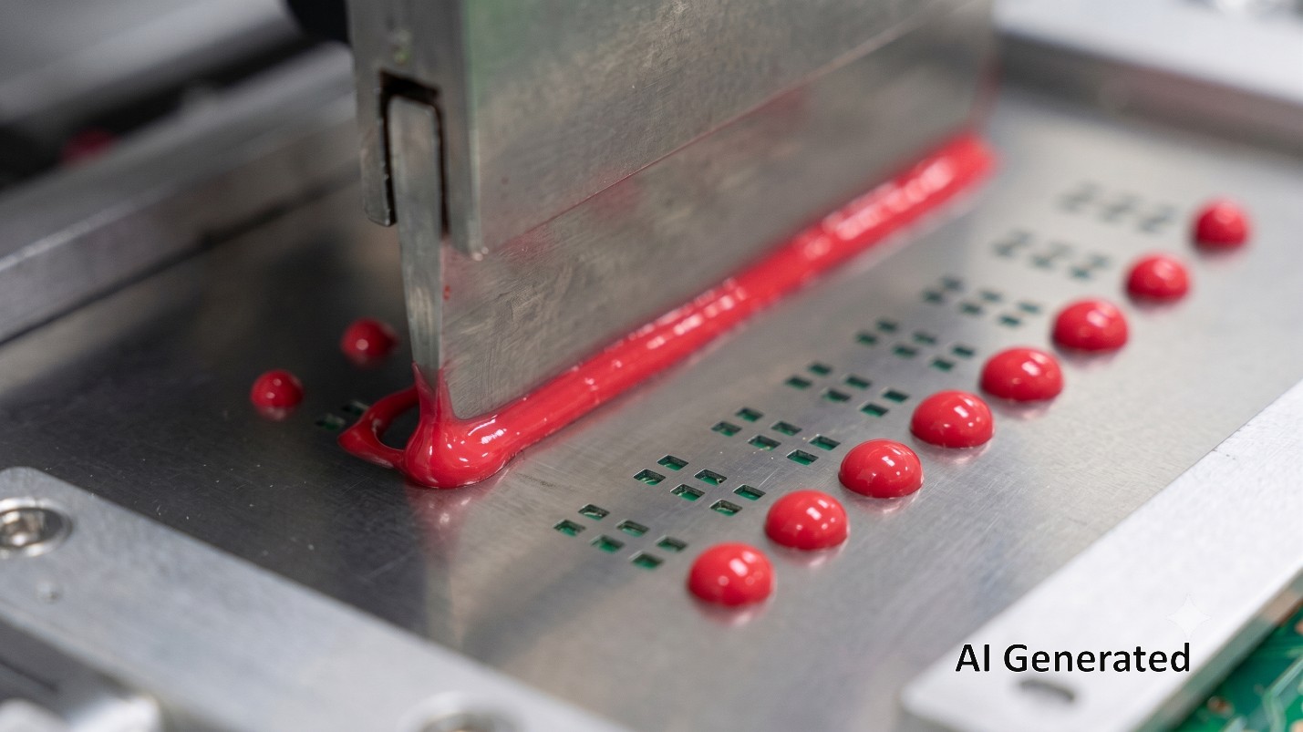
The Red Glue Stencil (when bottom-side SMD meets the wave)
For applications integrating bottom-side SMT and through hole on same board, the surface-mounted components that pass over the wave should be glued beforehand to avoid being washed off in the molten solder. In this case, a separate red-glue stencil deposits epoxy dots between/beside SMD pads under each bottom-side part. The thickness of the foil for this process should be around 0.15 – 0.30 mm so the dot clears the component standoff.
To ensure perfect alignment, the paste and glue stencils must reference the same PCB origin, ideally from one Gerber upload. JLCPCB supports both stencil types from one upload, preventing registration drift.
Design Rules for a Mixed PCB Assembly Board
Like other engineering products and prototypes, problems in manufacturing often emanate from poor design. Mixed board failures are no exceptions. Whether you are designing as an amateur or a seasoned mixed board designer, the subsequent guidelines can help in mitigating board failures during production.
Component Placement Rules
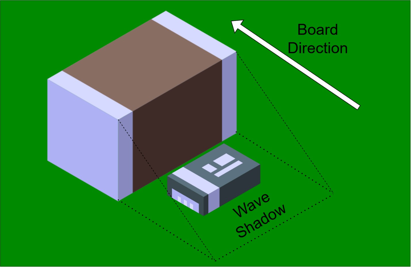
As mixed PCBs integrate SMT and through hole on same board, the placement of the components can also be a deciding factor for failure. To ensure both SMT and THT leads are soldered properly during the wave step, there should be a minimum clearance of 2.5 mm between SMT and THT. This gap ensures the wave solder can approach at an appropriate application angle. In addition to this, heat-sensitive SMT parts like connectors and plastic bodies must be placed away, if possible, from wave-soldered zones.
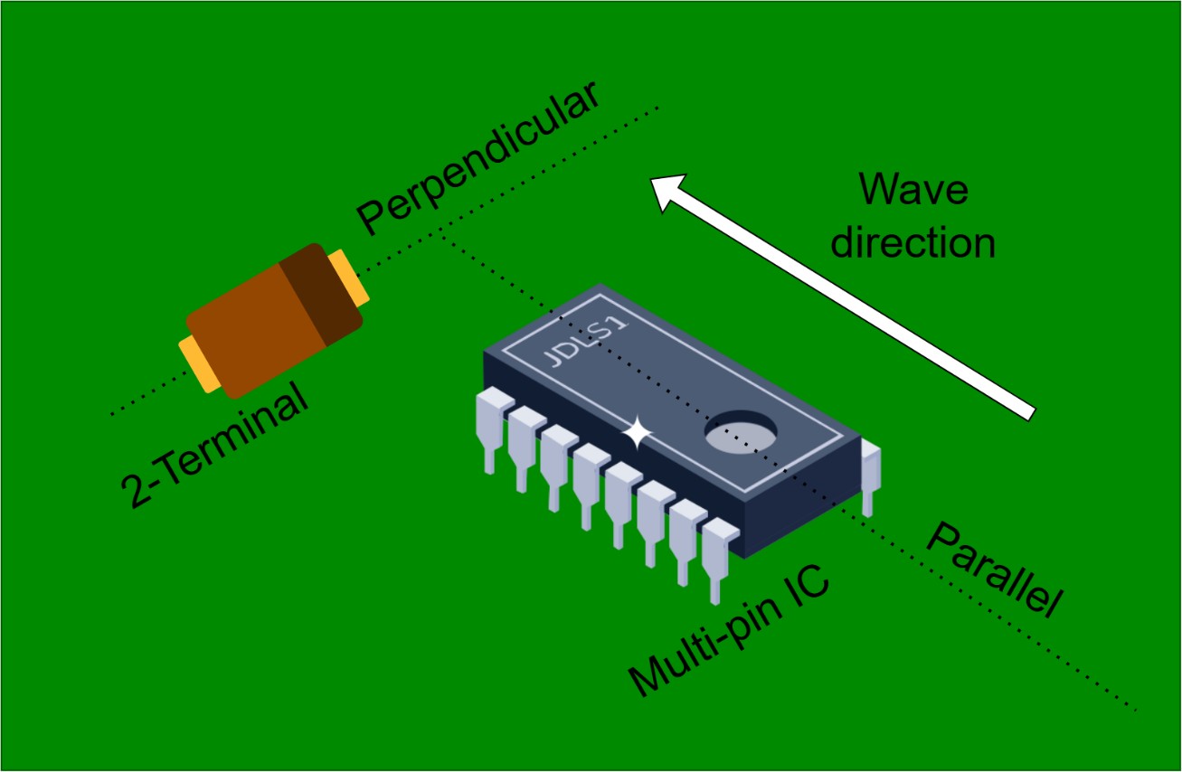
During wave soldering, the correct orientation of bottom-side SMD depends on the component type to prevent wave shadowing and incomplete soldering. For two-terminal chip components, the long-axis should be placed perpendicular to the wave path to ensure even soldering. Conversely, multi-pin ICs should be placed parallel to the wave direction to prevent solder bridging. Finally, it is good practice to group THT parts by lead direction, as rows of THT parts arranged in parallel are generally cheaper to auto-insert than scattered components.
Thermal Profile Considerations
Regardless of the sequence that you are going to use for your mixed board, each component must be able to withstand the thermal stress during reflow. For sequence A, which includes a standard reflow and wave soldering, the bottom-side SMD parts experience a second thermal cycle. Although the thermal peak profiles of the lead-free reflow (235 to 250 °C) and the wave bath (250 to 260 °C) are fairly close, the boards still perceive two heating cycles. Because of this, it is necessary to verify the thermal tolerance of the individual components for a second cycle in their respective datasheets.
In the same way, for sequence B employing Pin-in-Paste, careful verification of each THT component is necessary to assess reflow compatibility. Normally, the plastic parts of THT components do not experience high thermal stress during wave soldering. In Pin-in-Paste, however, since the THT parts are reflowed alongside the SMT parts simultaneously, they are subjected to the higher thermal profiles.
DFM Rules That Save You a Spin
In the electronics manufacturing industry, redoing a board, also referred to as a spin, costs time, money, and effort. As much as possible, the circuit board must be well-designed for manufacturing to save unnecessary spins arising from design failures or defects.
In sequence A, before sending bottom-side components through a wave bath, they need to be glued down first. This adhesive or glue layer, however, must be marked explicitly and separately in the Gerber, as many CAM systems generate the glue stencil directly from this specification. Failing to do so might cause the factory's automated CAM software to omit the glue stencil. On the other hand, for mixed PCBs expected to use sequence B or Pin-in-Paste, the Gerber must specify whether the barrels are paste-filled or left for wave soldering, as different stencils will be generated accordingly.
For boards mixing 0.4 mm BGAs with large connectors, requesting a design for manufacturing (DFM) review prevents failures early on from conflicting paste volume requirements. When mixing fine-pitch components with massive connectors, a custom step stencil is a must to ensure the board works as intended. Furthermore, for all parts above 0.5 mm, the standoff height must be indicated in the design process to guide the factory’s choice of glue-stencil thickness and step stencil specifications.
Common Challenges in Mixed PCB Assembly
| Problem | Solution |
|---|---|
| Thermal Stress: As SMT joints and THT components within the board endure thermal stress during heating cycles, whether in sequence A (reflow then wave) or sequence B (PIP), they experience expansion, which might lead to cracked joints or component failure. | The thermal profile alongside the ramp/cool rates must be strictly controlled. Each component must be verified to determine whether it can withstand second heating cycles whenever applicable. Furthermore, heat-sensitive components must be placed far away from harsh wave zones. |
| Second Reflow: Bottom-side SMD and PIP parts see a thermal excursion beyond their reflow rating, which could lead to the remelting or degradation of the solder joints. | To address this issue, verify each part’s peak temperature and second-reflow rating. For bottom-side SMD, proper glue-curing must be practiced. The sequence must be designed such that sensitive components are placed far from aggressive heating zones so they effectively see fewer heating cycles. |
| Glue (adhesive) failure: When using the standard sequence, bottom-side SMD can wash off in the wave treatment when the glue dots are improperly sized, placed, or cured. | To prevent this, the red-glue stencil thickness must be set properly so the dot clears the standoff height. The dots must also be carefully placed between and beside pads while applying full thermal/UV curing. |
| Wave shadow: Tall components can block the wave from downstream leads, causing weak joints, skips, and insufficient barrel fill. | The components must be placed at least 2.5 mm apart so that they get enough exposure from the wave. It is also recommended to place tall components downstream to avoid wave shadowing. If it is inevitable, selective soldering must be done for shadowed components. |
| Connector warpage: Large plastic connectors or the board itself can warp under wave or a high second-heat cycle, often leading to joint lifting or degradation. | To address this, the thermal profile must be set correctly to fall within the safe reflow temperature tolerance of the PIP components. For the board itself, managing the thermal mass and profile while installing fixtures or supports can prevent warpage. |
| Mixed BOM: Since a factory line supporting a mixed assembly process needs SMT reels, THT parts, and adhesives, sourcing becomes much more complicated. The bill of materials often can become messy alongside line changeovers, increasing the risk of human error. | To mitigate these challenges, it is recommended to consolidate suppliers, mark SMT and THT clearly in the BOM/CPL, plan feeder/insertion setup, and consider PIP to shrink the THT/wave BOM. |
FAQ about Mixed PCB Assembly
Q: How do I categorize and communicate Pin-in-Paste components to my PCB manufacturer?
You should classify and mark your Pin-in-Paste components as standard SMD parts in your design software and Bill of Materials. Next, you should ensure that the paste mask over the plated hole is opened in your design. As long as your component is supplied in a pick-and-place-friendly package, the manufacturing line can recognize it seamlessly as a PIP component.
Q: How to maintain clean pads during Pin-in-Paste?
There are several factors that can affect the cleanliness of pads during Pin-in-Paste. During reflow, to ensure that the paste does not spread out, the boards should be elevated by at least 2 mm from the mesh belt to prevent the mesh from touching the paste pad. Other things worth checking would be cleanliness and alignment of the stencil and pads.
Q: How to maintain rounded through-hole solder terminations for mixed boards?
For the Pin-in-Paste sequence, through-hole barrels can be properly filled when the right stencil apertures are used. Larger stencil apertures ensure enough solder paste is deposited to maintain rounded solder terminations. Meanwhile, for wave soldering sequences, the components must be oriented perpendicular (for two-terminal chips) or parallel (multi-pin ICs) to the wave travel path while respecting clearance guidelines (≥ 2.5 mm) to achieve rounded solder joints.
Q: Why are nano-coating and electropolishing important for stencils in mixed PCB assembly?
High-quality stencils are often nano-coated and electropolished to prevent solder paste from getting stuck and smearing underneath the stencil during long production runs. The nano coating allows for improved paste release while electropolishing ensures aperture walls are smooth. Furthermore, nano-coated and electropolished stencils prevent contamination and bridging defects during the subsequent wave soldering process.
Q: How is wave soldering different from selective soldering in hybrid PCB assembly?
Both wave and selective soldering can be applied to THT components in hybrid PCB assembly, but they differ mainly in their mechanism. Wave soldering subjects the entire bottom surface of the PCB to a large, continuously flowing pan of molten solder, establishing joints simultaneously. On the other hand, selective soldering typically makes use of an automated arm that moves from point to point to target specific components. Wave soldering is advantageous for mixed boards with a high number of THT components while selective soldering usually suffices for boards employing sparse THT parts.
Q: Where does an SMD glue stencil deposit adhesive?
The apertures for the SMD glue stencil are designed to target the space between the copper pads. Since the glue is designed only as an anchor and a non-conductive layer, it must be placed entirely away from the copper. The SMD glue stencil carefully deposits the adhesive on the solder mask directly underneath the component body to anchor it securely.
Conclusion: Treating Mixed PCB Assembly as a System, Not a Step
In conclusion, a mixed PCB assembly isn’t merely an SMT board with a few THT parts bolted in. It is a sequenced flow where every step affects the next. Implementing the right sequence (A vs PIP), stencil setup (paste + optional glue + step), design-for-manufacturing rules, and solutions to address common challenges altogether determine production yield. Missing or failing any of these can lead to mixed board failures.
To build a mixed PCB assembly properly and ensure perfect alignment, using a reliable stencil is a must. JLCPCB offers a wide variety of stencil services and products, developed for extensive PCB prototyping and trusted by millions of engineers worldwide. They produce paste and red-glue stencils on the same laser lines with ±0.003 mm precision, nano-coated/electropolished stencils, and step stencils. Their 12-hour build, unified Gerber upload, one-piece minimum order quantity, and $3 starting price provide everything you need to get started and make further iterations practical.
DFM mixed boards are now the default in the electronics industry. They can be a headache to produce without following the guidelines and the right sequence. Get the sequencing right, equip the line for both processes, and a mixed PCB assembly stops being where revisions happen and starts being where products ship.
Keep Learning
Low-Temperature Solder Paste: A Practical Sn-Bi Guide
Key Takeaways Sn42Bi58 is the mainstream low-temp alloy and melts at 138 C. Typical reflow peak is 165 to 180 C, about 25 to 30 C above the melt. It protects heat-sensitive components and reduces warpage on large, thin boards. It enables step soldering, because 165 to 180 C will not remelt SAC305 joints. Bismuth joints are more brittle than SAC305, so avoid drop-critical products. Never mix Sn-Bi with leaded (Sn-Pb) solder. Bi, Sn and Pb form a ternary eutectic that melts near 95 C. Some parts and som......
Pin-in-Paste: Through-Hole Reflow With a Stencil
Key Takeaways One Reflow Process: Pin-in-paste combines SMT and through-hole soldering into a single reflow pass, eliminating the need for separate wave, selective, or hand-soldering steps when the board has only a few through-hole components. Paste Volume Is Critical: Solder paste is roughly 50% flux by volume, so you need to print about twice the solder volume the finished joint requires. Stencil design—overprint apertures and step-up zones—makes or breaks the process. Target 75% Barrel Fill: Per IP......
Mixed Technology PCB Assembly: Combining SMT and THT on One Board
As technologies become increasingly more complex, the demand for sophisticated printed circuit boards continues to rise. In the electronics industry, the two most prevalent PCB Assembly technologies are SMT and THT, which differ mainly in the manner at which the components are attached. SMT places the components on the surface of the board whereas THT makes use of drilled holes to solder components. While these technologies individually cater to specific applications, advancements in the electronics i......
Moisture Sensitivity Level (MSL): Baking Guide
Key Takeaways Moisture Sensitivity Level (MSL) is a 1-6 classification under IPC/JEDEC J-STD-020 that indicates how quickly a non-hermetic surface-mount package can absorb enough moisture to become vulnerable during reflow. MSL 1 has unlimited floor life at its reference condition, while MSL 6 requires baking before use and reflow within the time printed on the caution label. The floor-life clock begins when the moisture barrier bag is opened and exposure to factory air starts. Baking according to IPC......
Understanding SMT Stencil Printers for Accurate PCB Solder Paste Printing
Stencil printing is a critical process in SMT (Surface Mount Technology) assembly, significantly impacting the quality and reliability of solder joints on PCBs. The crucial machine for implementing this is the SMT Stencil Printer, which applies an appropriate measure of solder paste to each pad of the PCB board before it goes to the placement of components. For those of you looking to work out what a stencil printer is and why it matters in manufacturing, you've come to the right place. This is the ba......
Surface Mount Stencil: A Practical Guide for SMT Printing and Solder Paste Application
It starts with a slim piece of metal, slipped in early during assembly. Before any part lands in place, before heat ever touches the board, that layer shapes the flow. Where the paste spreads comes down to its design. How thick it is, how it's cut - those details decide what sticks and what washes away. For engineers looking for reliable stencils, JLCPCB provides high-precision SMT stencils that integrate seamlessly with PCB production workflows. Down goes solder paste, slipping through narrow cuts in......