
How to Apply SMD Glue Using SMT Stencils (Design, Thickness & Troubleshooting Guide)
9 min
- Quick Answer: How to Apply SMD Glue in SMT
- How to Apply SMD Glue Using an SMT Stencil
- What Is SMD Glue and When Should You Use It?
- Essential SMT Stencil Design Rules for SMD Glue
- How to Order Your Custom SMD Glue Stencil From JLCPCB
- Frequently Asked Questions about SMD Glue Stencils
The reality of modern PCB assembly is that "mixed-technology" is still very much the norm. When a board hits the wave soldering machine, bottom-side SMD components face a high-velocity river of molten metal. Without a solid mechanical bond, they’ll simply wash away into the solder pot. That’s where the precision application of SMD glue becomes the difference between a successful run and a bin full of scrap.
Quick Answer: How to Apply SMD Glue in SMT
If you need to configure your SMT stencil for adhesive application immediately, follow these core parameters:
-
Stencil Thickness: Use a thicker foil of 0.15–0.20 mm to bridge the component standoff gap.
-
Aperture Design: Design round or oval apertures sized at 50–70% of the component body width.
-
Placement: Print glue strictly on the solder mask between pads, never on the copper.
-
Curing Profile: Cure the adhesive in an oven at ~150°C for 90–120 seconds.
-
Surface Finish: Utilize electropolished stencils to ensure consistent glue release and prevent stringing.
How to Apply SMD Glue Using an SMT Stencil
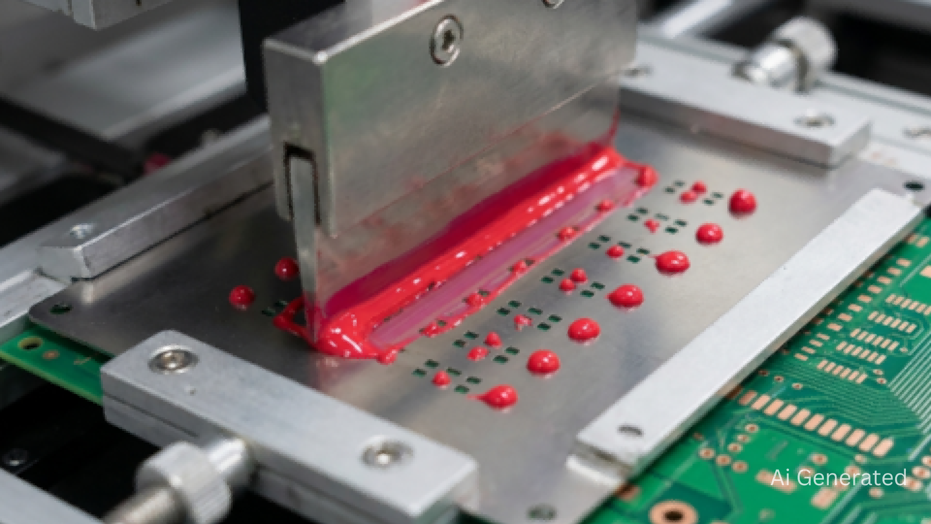
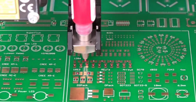
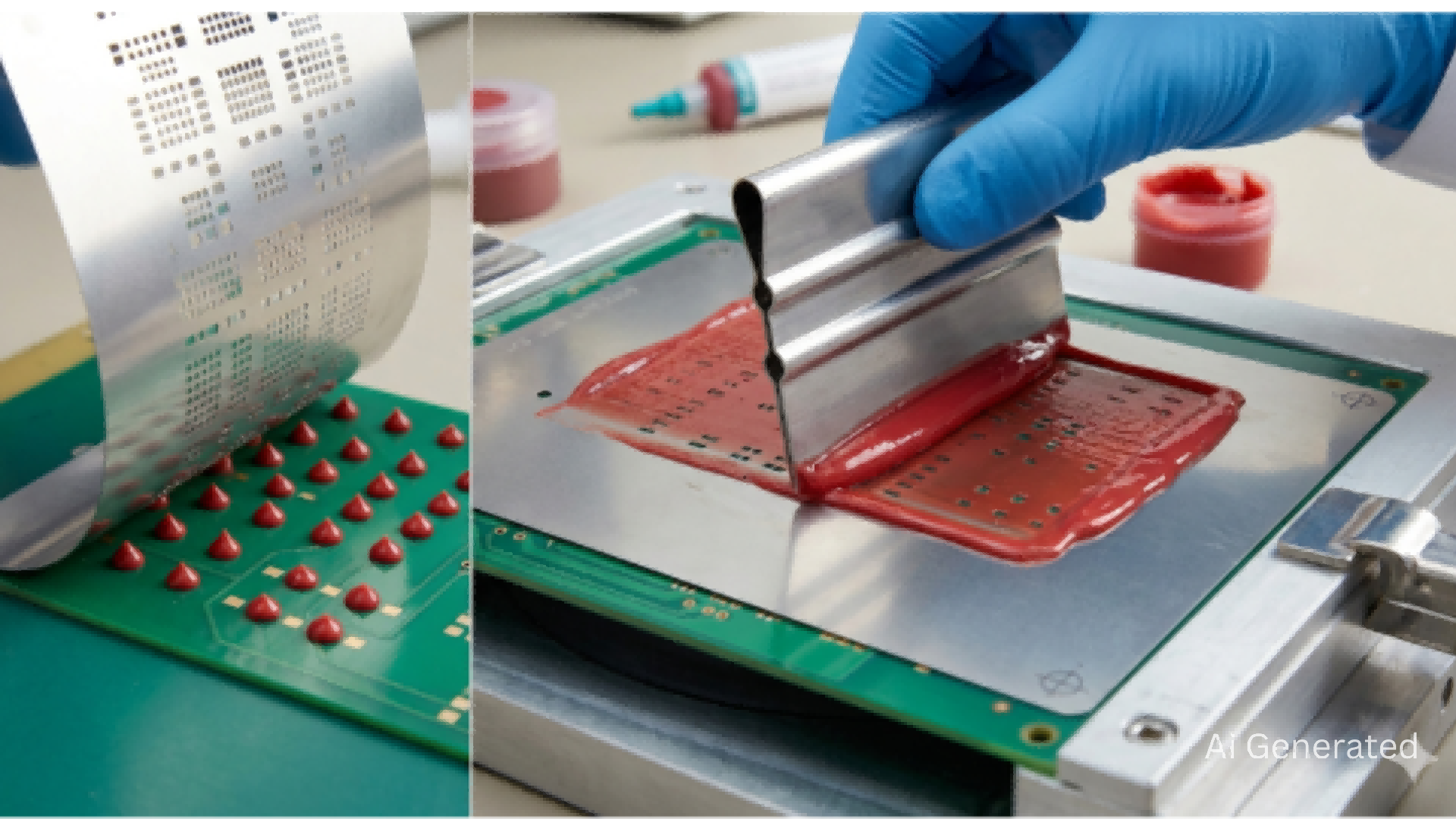
Applying the SMD glue with an SMT stencil happens in two significant steps. First is the printing process, and second is the curing that comes after the printing.
1The Printing Process
First of all, the custom stencil is aligned over the bare board, and a stainless steel squeegee drives the glue across the foil. Because glue is stickier than paste, using a slightly slower stroke speed and higher squeegee pressure works best. This ensures the glue fills the apertures completely. When the stencil lifts, the glue should form a crisp, peaked dot.
2Post-Print Curing
After the components are placed, the board must pass through a curing oven. This is usually a 150°C profile for about 90 to 120 seconds. This heat triggers the chemical reaction that hardens the epoxy. Once the board exits the oven, the parts are essentially "locked" until they reach the wave.
What Is SMD Glue and When Should You Use It?
What Is SMD Glue?
If you’ve spent any time on a shop floor, you probably know this material as "SMT red glue." SMD glue is classified as a single-component thermosetting epoxy adhesive. Also, unlike solder paste, which is meant to melt and flow, SMD glue is meant to Stay Put and will permanently harden once heat is applied to it.
Many practitioners favor the red and yellow varieties because they contrast better against the green or blue solder mask. It’s dyed red or yellow for AOI contrast, which allows inspection cameras to verify dot placement across hundreds of boards in a single hour.
Thermosetting epoxies, like SMD glue, are chemically cross-linked during the curing stage. Once it sets, it’s not going anywhere, even when it hits the 260°C heat of a solder wave.
To be clear: SMD glue is purely a mechanical anchor. It is non-conductive. Its only job is to act as a bridge between the component body and the bare PCB substrate. It doesn't assist with the electrical joint; in fact, if it gets onto the copper pads, it acts as an insulator and ruins the connection.
When to Use SMD Glue With an SMT Stencil?
The "why" behind using glue is almost always tied to the board’s physical layout. If you have components on both sides, but the board requires PCB wave soldering for the THT parts, you’re in the glue zone.
The workflow
The process is typically as follows: print glue on the bottom side, SMD parts, glue curing, board flipping, then insertion of THT components on the top side.
The bottom side SMD parts and THT components are soldered during the wave soldering and bottom side SMD soldering processes at the same time. The glue is what keeps those bottom-side parts from falling off into the molten lead-free alloy while they are submerged.
Why use a stencil?
A lot of people try to use a manual dispenser or a syringe for this. For prototyping, manual pneumatic dispensing with a syringe is fine. It is slow, and the dot volume varies by operator, but for a small run, it gets the job done. At production volumes, that variability becomes a defect source
That’s where stencils turn out to be a necessity. A laser-cut SMT stencil eliminates the inconsistency. Every aperture deposits the same volume at the same location, every cycle. That determinism is what makes high-speed, zero-defect assembly possible.
Essential SMT Stencil Design Rules for SMD Glue
Designing the perfect SMT stencil for SMD glue requires some expertise that many lack. Here are two crucial tips on SMT stencil design that help a lot.
SMD Glue Stencils vs. Solder Paste Stencils
To ensure high-yield manufacturing, engineers must distinguish between the design requirements of these two distinct tools. Using the wrong stencil leads to immediate component washout or electrical failure.
The key distinction is that they come from different Gerber layers and deposit material at completely different locations on the board.
- A solder paste stencil is derived from the SMD paste layer. Here, the apertures sit directly over exposed copper pads, where solder needs to wet and form joints.
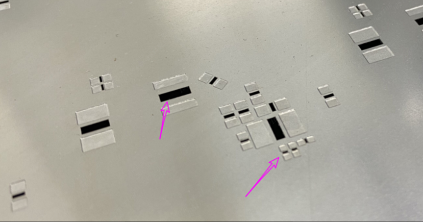
- An SMD glue stencil is derived from a separate adhesive layer. In this case, apertures target the solder mask between the pads, underneath the component body, away from the copper entirely.
Pro Tip
Always validate adhesive Gerbar against the component footprint overlay before ordering anything
Stencil Thickness
Standard paste stencils run 0.10–0.12mm thick. Adhesive stencils need more, because the glue dot has to bridge the Z-axis gap between the PCB surface and the underside of the component body.
If the dot is not tall enough to contact the component when it is placed, the bond is already compromised before curing. Specify 0.15–0.20mm foil thickness for adhesive stencils. Larger or heavier components may push toward the upper end or require a step stencil configuration.
Stencil Aperture Shape and Volume
Round or oval apertures are the right choice for SMD glue. They release cleanly as the stencil separates. Rectangular apertures trap material in corners, leading to inconsistent dots and stringing.
On sizing, target roughly 50–70% of the component body width. Too small, and the dot misses the component body. Too large, and placement forces glue onto adjacent pads.
Treat that range as a starting point and validate with print trials on test boards. Different adhesive viscosities require different values.
Troubleshooting Common Defects in SMD Glue Printing
Diagnosing issues on the line usually comes down to understanding cause and effect.
-
Pad Contamination
This is the defect that matters most. Glue on a copper pad is an electrical insulator sitting exactly where solder needs to wet. During wave soldering, that pad produces a void or an open joint, a failure that AOI may not catch if the component body obscures the pad.
-
Missing or Inconsistent Dots
Missing dots are almost always a release problem, clogging, stringing, or rough aperture walls holding material back during stencil separation. The best engineering solution is electropolished stencil foil.
The Importance of Precision Manufacturing
When you're moving from a prototype to a real production run, the precision of your stencil is the only thing that stands between you and a massive rework bill. Poorly cut apertures lead to stringing; incorrect thickness leads to weak bonds that fail in the wave.
To eliminate these variables, professional environments rely on stencils manufactured via high-precision laser cutting. When combined with an electropolished surface finish, the aperture walls become ultra-smooth, ensuring the sticky adhesive releases perfectly every single time.
How to Order Your Custom SMD Glue Stencil From JLCPCB
JLCPCB builds custom stencils using high-grade 304 HTA stainless steel with a strict cutting tolerance of ±0.003mm. Their automated system allows you to easily select thicker foils (0.15mm and up) that are specifically suited for the standoff height of SMD glue applications.
Pros
- Starting price: Just $3 USD
- No Minimum Order Quantity: (MOQ: 1)
- Speed: Production can be completed in as fast as 12 hours.
Whether you need a simple frameless foil for a benchtop setup or a large framed stencil for an automated line, JLCPCB removes every practical barrier between a correct design and a reliable board.
Choose from Framed/Frameless, Electropolishing, Nano-coating, Step-Stencils, SMD Glue Stencil and more. Starting at $3. No MOQ. 12-Hour production.
Get $11 Coupon Now >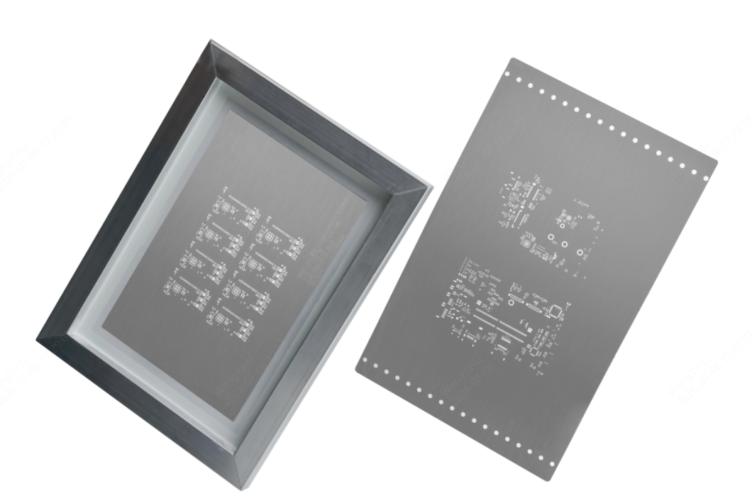
Frequently Asked Questions about SMD Glue Stencils
Can I use my solder paste stencil for SMD glue?
No. Solder paste stencils are usually too thin (0.10mm) to bridge the component standoff gap, and the apertures are located on the pads rather than between them. Using one will lead to component washout and failed electrical joints.
Why is my glue "stringing" when the stencil lifts?
Stringing is usually caused by the glue being too cold or the stencil separation speed being too fast. Ensure your glue has reached room temperature before printing, and slow down the vertical lift speed of your printer.
How do I clean a stencil after using SMD glue?
Don't let it dry. Use IPA (Isopropyl Alcohol) or a specialized aqueous stencil cleaner immediately after the production run. If the glue cures inside the apertures, the stencil is effectively ruined.
Is SMD glue necessary for all double-sided boards?
No. It's only necessary if you are using wave soldering. If you are doing a double-sided reflow process (where you use solder paste on both sides and pass through a reflow oven twice), the surface tension of the molten solder is usually enough to hold small parts in place on the bottom side without glue.
All in all, SMD glue application is one of those process areas where small errors upstream produce expensive failures downstream. Get the Gerber apertures right, specify the correct foil thickness, validate with print trials, and run a complete cure cycle before wave soldering.
A precision custom SMT stencil from JLCPCB is the fastest way to lock those variables in at production scale. The $3 price, with no minimums, and a lead time as fast as 12 hours, removes every practical barrier between a correct design and a reliable board.
Keep Learning
SMT Stencil Cleaning Guide: Process, Frequency, and Tips
Key Takeaways about SMT Stencil Cleaning SMT stencil cleaning removes solder paste residue from aperture walls and the stencil underside, keeping paste transfer efficiency between 80% and 100%. Industry analysis attributes over 60% of SMT defects to the paste-print step — most of which trace back to a stencil cleaning lapse. Two stages matter: under-screen cleaning (between cycles, typically every 5–10 prints) and off-line cleaning (after production completes). IPA handles standard flux residue; dedic......
Top 5 Circuit Board Stencil Mistakes & How to Fix Them for Higher SMT Yield
Usually, the circuit board stencil is responsible for roughly 60% to 70% of all SMT defects. That number surprises people. It shouldn't. The stencil controls paste volume, deposit geometry, and positional accuracy all at once. When it gets wrong, everything downstream pays for it. The shift in thinking that separates good engineers from great ones is simple: stop seeing the PCB stencil as a metal sheet with holes in it. It is a precision fluid delivery system. Every aperture wall, every micron of foil......
How to Apply SMD Glue Using SMT Stencils (Design, Thickness & Troubleshooting Guide)
The reality of modern PCB assembly is that "mixed-technology" is still very much the norm. When a board hits the wave soldering machine, bottom-side SMD components face a high-velocity river of molten metal. Without a solid mechanical bond, they’ll simply wash away into the solder pot. That’s where the precision application of SMD glue becomes the difference between a successful run and a bin full of scrap. Quick Answer: How to Apply SMD Glue in SMT If you need to configure your SMT stencil for adhesi......
The Essential Guide to SMT Stencils in PCB Assembly
Introduction In the dynamic world of electronics manufacturing, Surface Mount Technology (SMT) plays a crucial role in achieving efficiency and precision in printed circuit board (PCB) assembly. Central to the SMT process is the SMT stencil, an indispensable tool for the accurate application of solder paste. This ensures solid electrical connections between components and PCBs. This guide delves into the specifics of SMT stencils, examining their types, materials, manufacturing methods, advantages, ch......
Nano-Coatings in PCB Manufacturing: How They Outperform Traditional Stencils
Nano coating is a thin hydrophobic (water repellent) and oleophobic (oil repellent) treatment used on the undersides and edges of solder paste stencils. With this the surface becomes non-stick which reduces the number of cleaning cycles required for the solder paste printing process. Upon application, the less than 5 nanometer coating bonds with the stencil foil at the microscopic level, which does not change the size and shape of the stencil. Nano coating is an industry proven process which shows imm......
How to Choose an SMT Stencil
What is an SMT stencil? SMT Stencil is a thin metal sheet used in the soldering process for SMT (Surface Mount Technology) and it plays an essential role in the SMT soldering process. Smt Stencil allows the direct placement of solder paste onto the SMD pads of PCB, which can help prevent errors and defects during the reflow soldering process. This results in a precise amount of tin coverage once the work is completed. Types of SMT Stencils Depending on the application of solder paste, there are three ......