
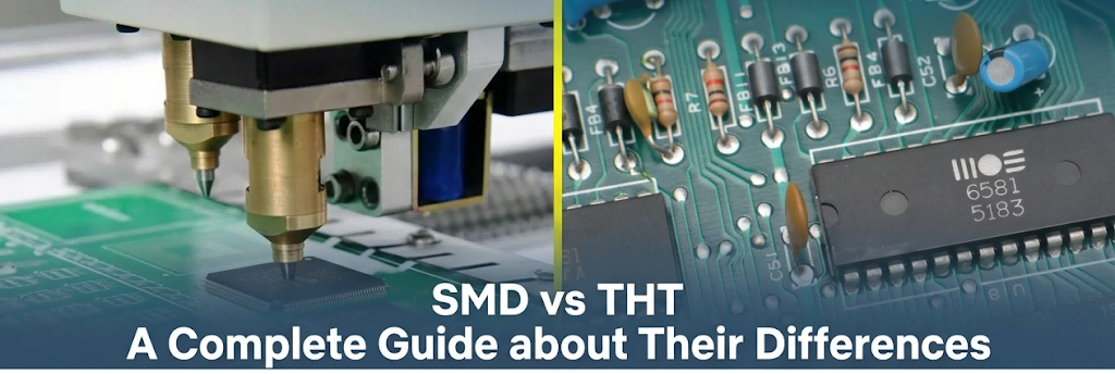
SMD Assembly vs THT Assembly: A Practical Guide
18 min
- SMD vs THT Assembly at a Glance
- How SMD and THT Assembly Work Differently
- Why SMT Relies on Stencil Precision
- Mixed-Technology PCB Assembly and SMD Glue Stencils
- Common SMT Defects and How Stencils Prevent Them
- Choosing the Right Assembly Method
- From Prototype to Production With JLCPCB
- FAQs: SMD Assembly vs THT Assembly & Mixed-Tech
- Conclusion: Mastering SMD Assembly vs THT Assembly with Precision Stencils
Every PCB design eventually faces the same fork: should this part be SMD or THT, and what does that choice actually mean for the manufacturing line?
The distinction between SMD and THT assembly extends far beyond component selection. It requires two completely separate manufacturing toolchains and introduces entirely distinct defect modes.
For mixed-technology layouts, a critical intermediate step is the bottom-side adhesive process. This stage involves dispensing precise dots of thermosetting epoxy to anchor surface-mount parts to the substrate, keeping components secure before the board passes through wave soldering. Without this step, the turbulent, molten solder wave will dislodge the parts.
This guide covers how each assembly workflow actually runs, what role the stencil plays in SMD yield, what mixed-tech boards quietly depend on, and how to choose between them.
SMD vs THT Assembly at a Glance
-
SMD assembly uses surface mount technology to mount components onto surface pads using solder paste, a precision stencil, and reflow soldering.
-
THT assembly inserts leaded components through plated holes, joined with wave, selective, or hand soldering — no paste stencil required.
-
Modern boards are practically exclusively mixed technology: SMD for density, THT for connectors, transformers, and hefty parts.
-
Bottom-side SMD on mixed boards needs an SMD glue stencil to fix components before wave soldering — the step most articles skip.
-
60–70% of SMD assembly defects originate at the paste-printing step (IPC data), making stencil quality the dominant yield variable.
-
THT has no equivalent single-point bottleneck; the plated barrel and wave process self-correct minor variations.
How SMD and THT Assembly Work Differently
What Defines an SMD Component
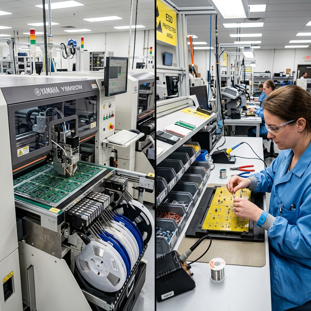
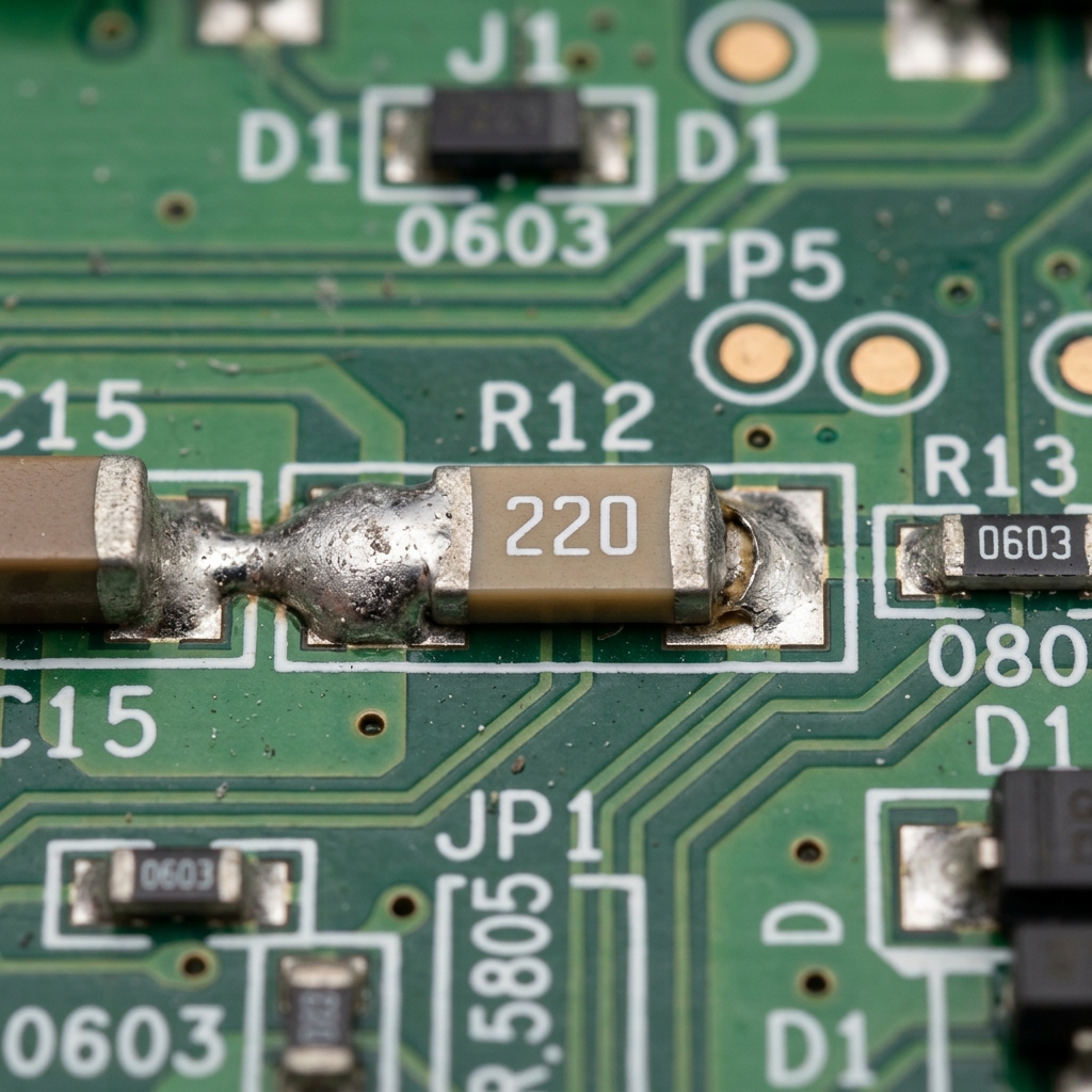
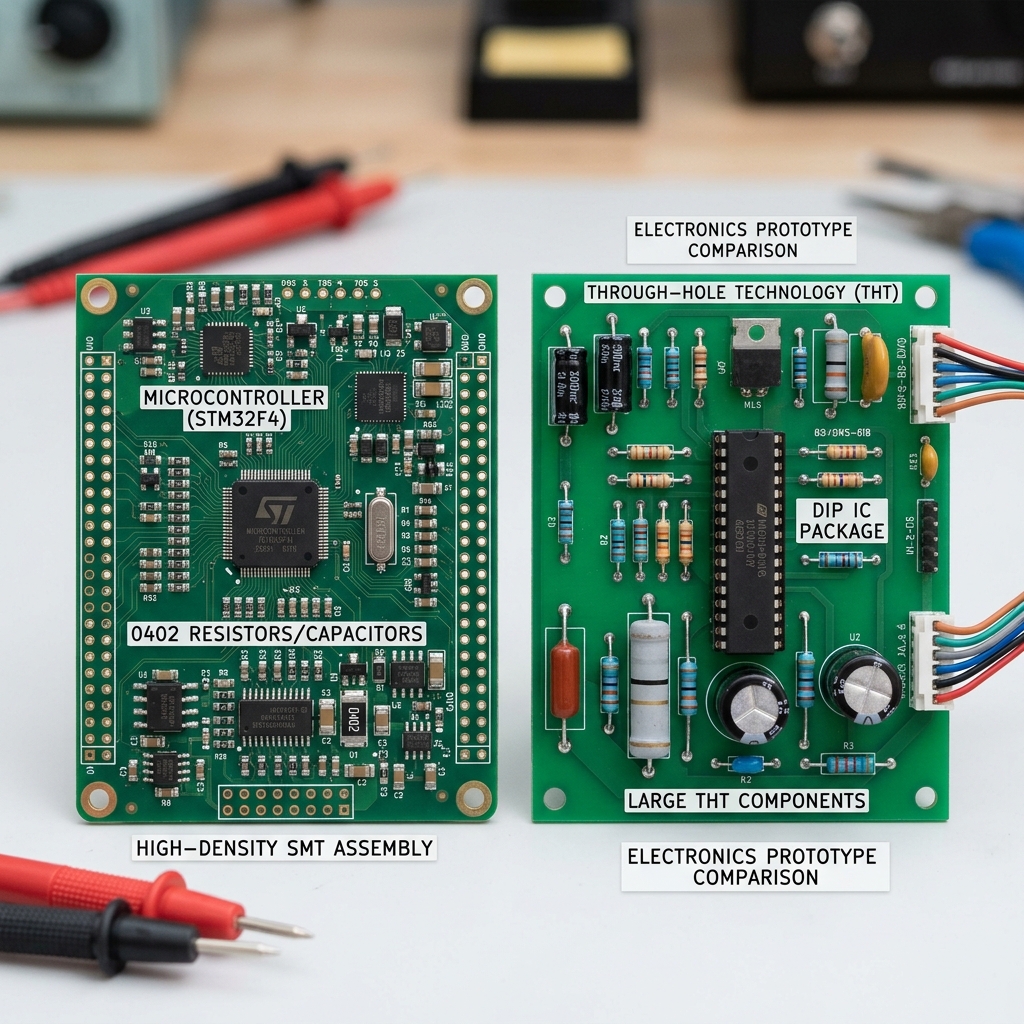
Surface mount technology defines a component family where no wire leads penetrate the board. Connection points are flat pads, lands, or solder ball arrays — from discrete passives (01005, 0201, 0402 sizes) up to integrated circuits in SOIC, QFN, LGA, BGA, and CSP packages. All require correct positioning with a solder paste stencil, pick-and-place robotic assembly, and a controlled reflow profile for reliable solder joints.
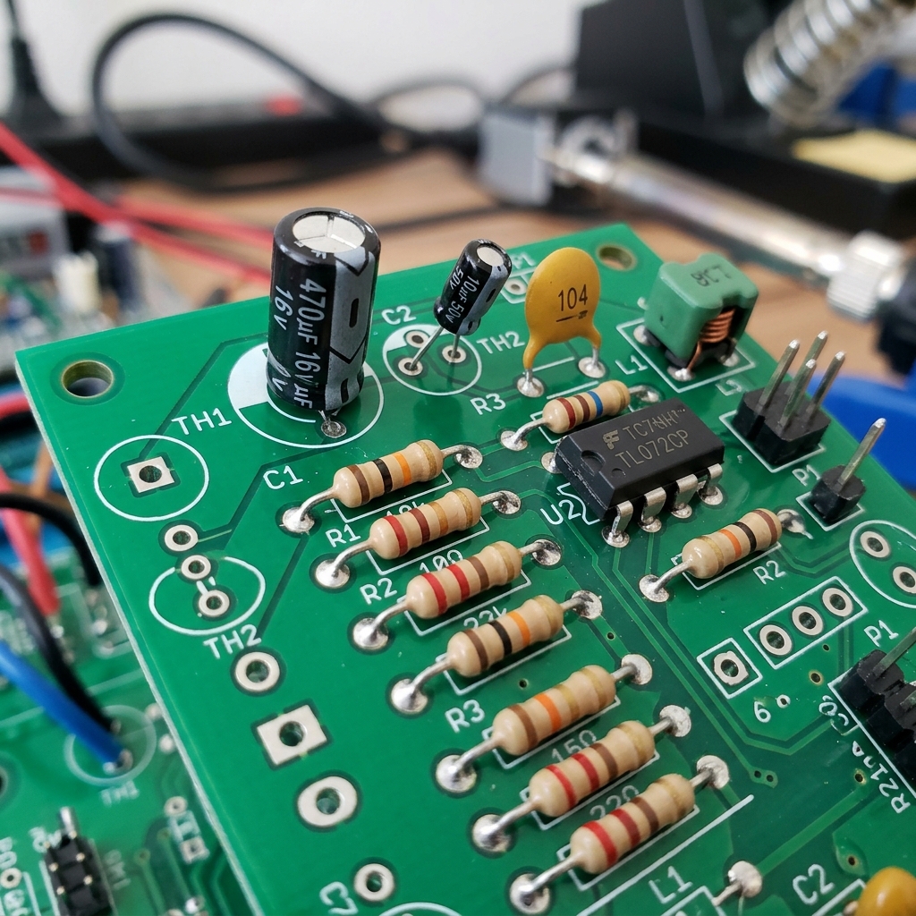
What Defines a THT Component
Through-hole parts have stiff metal leads that pass completely through plated holes in the board. Common through-hole components include DIP ICs, transistors (TO-220), radial electrolytic capacitors, terminal blocks, and large inductors. After insertion, joints are formed by wave soldering, selective soldering, or hand soldering — no paste stencil required.
The SMD Assembly Workflow
The standard SMT line operates as a tightly synchronized, linear thermodynamic system:
-
Solder Paste Printing:
Solder paste is driven through the apertures of a laser-cut stainless steel stencil by an automated squeegee blade onto the PCB pads.
-
Vacuum Pick & Place:
High-speed robotic placement heads extract components from tape reels or trays via vacuum nozzles and position them onto the wet paste.
-
Reflow Oven Thermal Profiling:
The populated board travels through a multi-zone conveyor oven. The thermal profile is divided into four critical metallurgical phases:
-
Preheat Zone: The assembly ramps up uniformly at 1–3°C/s to prevent thermal shock and begin activating flux chemistry.
-
Soak Zone: The flux activator chemistry — organic acids for no-clean flux, rosin acids for RMA — chemically reduces surface oxides on both copper pads and alloy powder particles. The soak plateau also thermally equilibrates high-mass THT connectors or heatsink-connected pads relative to small passives, reducing ΔT across the assembly to <10°C before reflow begins.
-
Reflow Zone: The alloy crosses liquidus (183°C for Sn63Pb37, 217°C for SAC305) and briefly reaches peak temperature. Typical peak targets are 205–215°C for SnPb and 235–250°C for SAC305. Time Above Liquidus (TAL) is controlled to 45–75 seconds. Insufficient TAL produces cold, grainy joints with incomplete intermetallic compound (IMC) formation (Cu₆Sn₅, Cu₃Sn at the copper interface). Excessive TAL grows a thick, brittle IMC layer (>3 µm Cu₃Sn) that reduces joint fatigue life under thermal cycling.
-
Cooling Zone: Forced convection cooling pulls the board temperature below the liquidus at 3–6°C/s. Faster cooling produces a finer, more fatigue-resistant microstructure. SAC305 joints cooled too slowly develop large β-Sn grain colonies prone to early crack initiation under thermal cycling.
-
-
AOI and X-ray Inspection:
4.Automated Optical Inspection uses multi-angle cameras with angled LED illumination to evaluate solder fillet geometry, component presence, polarity, and coplanarity. X-ray (2D or 3D CT) is required for BGA, LGA, and QFN packages where the solder joints are entirely hidden beneath the component body. X-ray reveals voiding percentage, bridging between solder balls, and missing balls.
Every downstream step in this process depends entirely on the accuracy of the first paste-printing step. If the solder paste volume or registration is incorrect, no downstream process can fully recover the joint.
The THT Assembly Workflow
THT assembly relies on entirely distinct mechanical and fluid dynamic stages:
-
Insertion:
Leaded parts are populated from the top side (Component Side) of the board into the through-holes. This is achieved via automated axial/radial insertion machinery or manual operator placement.
-
The Fluid Mechanics of Wave Soldering
The populated board moves along a conveyor tilted at a specific angle through three sequential stages inside a wave soldering machine:
-
Flux Application:
The underside of the board passes over a spray or foam fluxer. A precise volumetric coating of liquid flux is applied to break down surface oxides inside the plated barrels. Solid content deposition must be tightly managed to prevent excessive corrosive residues.
-
Thermal Preheating:
Forced-convection or infrared (IR) preheaters ramp the assembly up to a bottom-side temperature of 100° to 130° . This stage drives off the liquid volatile carriers (alcohol or water) in the flux, prevents thermal shock when hitting the molten metal, and activates the chemical rosins or organic acids.
-
Wave Dynamics:
The board contacts a molten solder pot maintained at 250° to 260°. It first hits a turbulent wave (chip wave), which uses high vertical fluid velocity to force solder into tight geometries and drive out pockets of trapped flux gas. It is immediately followed by a smooth laminar wave. This second wave provides a stable, low-velocity contact zone that allows the alloy to pull back cleanly from the pins. This mechanism relies on a controlled peel-back angle to prevent bridging. Total dwell time across both waves is limited to 2–4 seconds.
-
-
Lead Trim and Inspection:
Protruding component leads are trimmed to length if not pre-cut. Joint quality is evaluated against strict standards like IPC-A-610. This ensures the solder fills the vertical hole barrel completely and forms acceptable top-side and bottom-side fillets.
Manufacturing Equipment That Distinguishes the Two
SMT Toolchain: Screen printers, 3D Solder Paste Inspection (SPI) machines, high-speed chip shooters, multi-zone reflow ovens, and 3D AOI/AXI systems. This line demands higher initial CapEx but scales to massive component densities.
THT Toolchain: Axial/radial insertion machines, bulk wave solder pots, automated selective soldering cells (which use targeted, miniature solder pumps for individual pins), and manual rework stations.
Reliability, Strength, and Repairability
THT joints function as robust mechanical rivets. The lead passing through the plated barrel distributes structural stress across the entire inner cylinder of the PCB. This makes THT ideal for assemblies subject to severe vibration, thermal shock, or high mechanical insertion forces (e.g., connectors and power stages).
SMD reliability relies entirely on surface adhesion. Heavy components may require secondary epoxy structural reinforcement. However, SMD excels in high-frequency applications due to its lower parasitic inductance and capacitance.
For rework, THT can be desoldered using standard vacuum wicks or specialized thermal extraction tools. Conversely, fine-pitch SMD devices like BGAs and CSPs require dedicated hot-air rework stations, precise thermal profiles, and custom alignment optics.
Cost and Throughput at Volume
At high production volumes, SMT provides superior throughput. Automated placement systems can exceed 50,000 components per hour (CPH).
For low-volume, single-unit prototypes, THT can occasionally bypass the upfront lead times and engineering costs of fabricating custom stencils. When dealing with mixed-technology boards running 100 to 1,000 units per month, balancing the economics of both lines becomes a core manufacturing priority.
Why SMT Relies on Stencil Precision
Where SMD Assembly Defects Actually Come From
Industry Analyses Suggest : 60–70% of SMD defects originate at the paste-printing step, not placement, not reflow. Once the paste volume or registration fails, downstream processes cannot recover the joint. High Volume Lines use 3D Solder Paste Inspection (SPI) machines within a few seconds after the printer to detect anomalies before placing, avoiding expensive post-reflow rework.
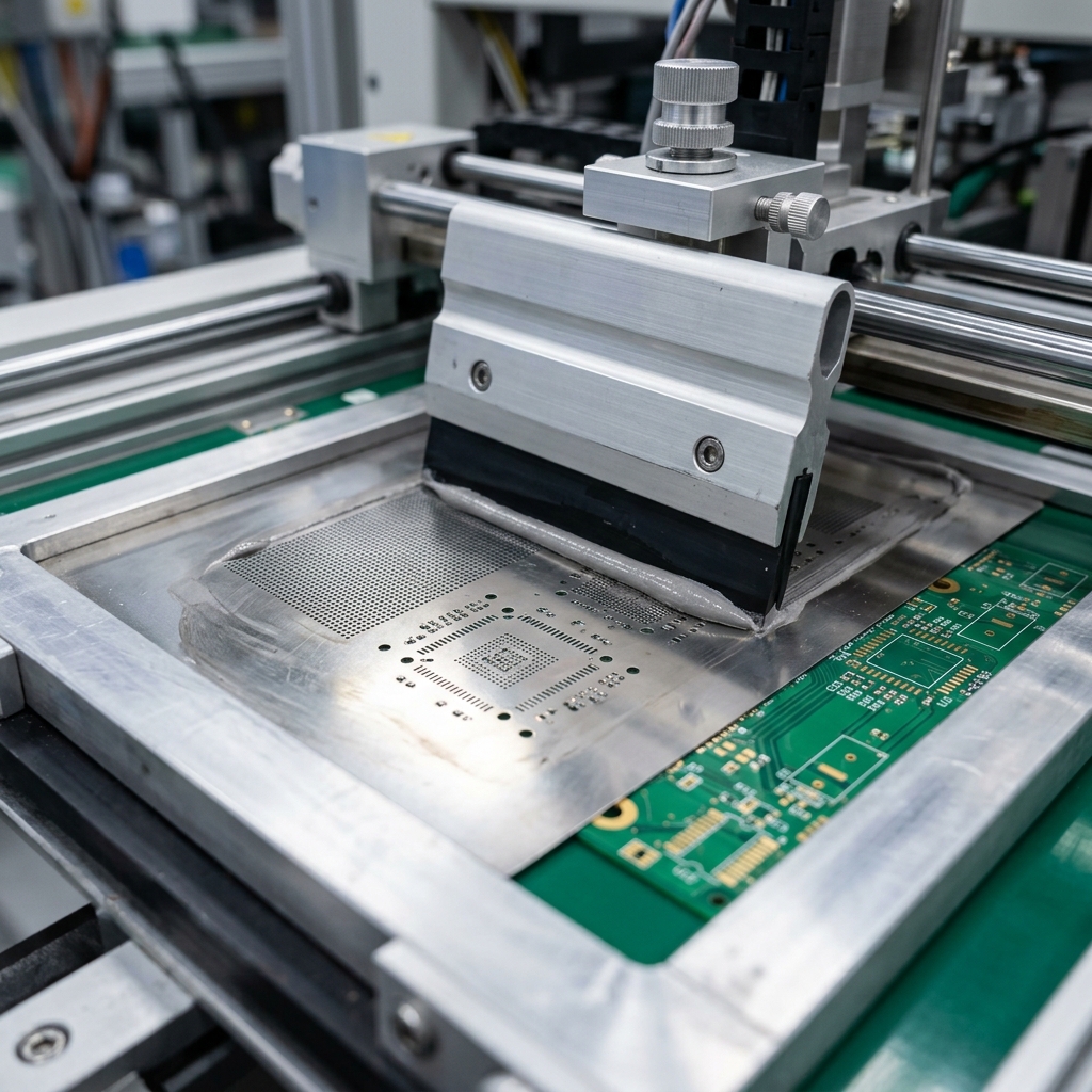
What the Solder Paste Stencil Controls
The solder paste stencil controls three critical variables simultaneously:
- Volumetric Consistency: Regulated by foil thickness and aperture area.
- Geometric Fidelity: Managed by aperture wall roughness and corner radii.
- Registration Accuracy: Controlled by alignment mechanisms within the printer.
Solder paste acts as a thixotropic suspension. Under the mechanical shear stress of a moving squeegee blade, its viscosity drops drastically, allowing it to flow into the tiny apertures of the stencil.
The moment the squeegee passes, the shear stress drops to zero. The paste must instantly recover its viscosity to stand tall without slumping. When working with fine-pitch components, 0.4mm pitch BGAs or 0201 passives, the stencil must meet tight tolerances of 0.01mm.
Stencil Specs Worth Knowing
To ensure predictable paste release when the stencil lifts off the PCB, engineers use the Area Ratio calculation. Per the IPC-7525B standard, this ratio must be greater than or equal to 0.66:
AR = Area of Aperture Opening/Area of Aperture Walls = W x L /2T (W + L) 0.66
Where: W = Aperture Width, L = Aperture Length, T = Stencil Foil Thickness
-
Foil Thickness:
Standard values run from 0.10mm to 0.12mm for fine-pitch SMT, and up to 0.15mm for larger, mixed-density packages.
-
QFN Thermal Pads:
These use "window-pane" or cross-hatched grid aperture patterns rather than a solid 1:1 opening. This provides open pathways for volatile flux gases to escape, preventing the component from lifting and reducing large solder voids.
-
0201 Passives:
These often employ "home-plate" or "U-shape" aperture geometries. This design pulls the paste away from the inner edges, minimizing the risk of tombstoning.
Why THT Has No Equivalent Bottleneck
THT joints form inside a plated barrel. Capillary action can be used to compensate for minor solder positioning errors and flux variation by sucking molten solder into the cavity. Eliminating process variation cannot be done, which is why THT lives on in legacy, high-reliability, high-power applications.
Mixed-Technology PCB Assembly and SMD Glue Stencils
Why Real-World Boards Are Almost Always Mixed-Tech
Very few commercial products use pure-SMD or pure-THT boards. Common designs use SMD for all high-density devices, such as memory, passives, and high-density microprocessors, and they keep THT for mechanical devices, like barrel jacks, electrolytic capacitors, transformers, and user-facing switches. There is a need for a plan to run two soldering processes simultaneously on a board for all mixed-tech builds.
The Mixed-Tech Build Sequence (Where SMD Glue Enters)
Processing a dual-sided mixed-technology board requires a precise assembly sequence:
Top-Side SMT
Solder paste is printed on the top side of the board. Components are placed via pick-and-place and processed through standard reflow ovens.
Board Inversion
The board is flipped 180° to expose its unpopulated bottom side.
Adhesive Screen Printing
A specialized SMD glue stencil applies dots of thermosetting epoxy (often called "red glue") directly onto the substrate mask, centered between the SMT landing copper pads.
Bottom-Side Placement and Curing
Bottom-side SMD passives and ICs are pressed into the wet glue dots. The board then passes through a thermal curing oven (or an IR line) to polymerize the adhesive, locking the components firmly to the epoxy layer.
Board Re-Inversion & THT Stuffing
The board is flipped back right-side up. THT components are stuffed from the top side, allowing their long metal leads to project out through the plated holes on the bottom side.
Wave Soldering
The entire bottom surface of the board passes over the molten solder wave. The wave simultaneously completes the through-hole joints and plates the exposed leads of the glued bottom-side SMDs.
Without this critical adhesive, the bottom-side SMD components would melt and fall directly into the wave solder pot, reaching temperatures of 250°C to 260°C.
How a Glue Stencil Differs From a Paste Stencil
| Parameter | Paste Stencil | Glue Stencil |
|---|---|---|
| Aperture position | Over copper pads | Between pads, under the component body |
| Aperture shape | Rectangular / pad-matched | Round dots sized to the component body |
| Thickness | 0.10–0.15 mm | 0.15–0.30 mm |
| Cleaning cycle | Solvent-compatible | Abrasive; more frequent |
Dot diameter targets 50–70% of the component body width. Larger packages like SOICs and QFPs need 2–4 dots to resist rotation under the solder wave. Glue that overflows onto adjacent copper pads prevents wetting and kills the joint.
Common SMT Defects and How Stencils Prevent Them
Insufficient Solder on SMD Pads
The following are just some solder paste printing defects that can happen: poor gasketing of the stencil to the board, too little or too high a squeegee pressure, bringing too cold or unmixed solder paste, or an oxidized pad finish. When the Aperture Area Ratio is < 0.66, paste sticks to the interior of the aperture, which leads to the stencil clogging and failure to release the paste completely.
Fixes: Increase squeegee pressure, clean the stencil more often, ensure the Area Ratio is greater than 0.66 as per IPC-7525B, consider the upgrade to electropolishing or nano-coating process to reduce surface friction.
Bridging Between Fine-Pitch SMD Leads
Joining the fine pitch SMD leads together. Too much pressure on the squeegee, squeezing paste under the stencil, excessive reflow ramp speed, or inadequate clamping of the board. Stencil apertures too large over the component pitch or a loose stencil, or an over-dusted stencil underside.
Fixes: Apply a 10%-20% aperture width reduction on fine pitch leads to avoid the bleed of paste on the leads and manage the squeegee pressure and an increase of the cleaning cycle of the under-stencil wipe with an automated system to control the frequency.
Tombstoning on 0201 / 0402 Chip Components
Asymmetric heating in the reflow oven, uneven trace routing acting as a heat sink on one pad, or placement misalignment. Uneven paste volumes are deposited on the two matching pads of a passive component, often due to localized stencil wear or clogging.
Fixes: This includes making sure to balance the reflow profile, redesign stencil apertures with "home-plate" or "U-shape" geometries to minimize paste usage at the inner edges of the aperture, and perfect print registration.
Voiding Under BGA and QFN Thermal Pads
The large, solid pieces of solder paste hold the flux solvents out-gassed under the entire body of the component during the reflow, forming enclosed air pockets.
Stencil-side Fix: Avoid printing a solid 1:1 paste block. Apply a "window-pane" or cross-hatched grid aperture pattern with a minimum grid spacing of 0.3mm. This provides channels for volatiles to escape cleanly while maintaining sufficient solder coverage.
Component Shift After Wave Soldering (Mixed-Tech Specific)
Insufficient or misregistered SMD adhesive holding bottom-side components, or incomplete adhesive curing.
Glue-stencil Fix: Increase the glue-stencil aperture diameter transition to a multi-dot layout for longer packages, and verify alignment with the component centerline.
Choosing the Right Assembly Method
When SMD Assembly Is the Right Choice
Surface mount technology is the optimal choice for:
- High-Density Requirements: Essential for designs using fine-pitch BGAs, QFNs, LGAs, or ultra-small passives.
- High-Frequency Signal Performance: Lowers parasitic trace inductance and capacitance, which is critical for RF, high-speed digital lines, and microwave designs.
- High-Volume Scale: Automated SMT lines maximize throughput and lower the per-unit cost at volume.
When THT Assembly Is the Right Choice
Here’s when THT assembly works perfectly –
- Mechanical Stress Environments: Ideal for heavy-use connectors, user-facing switches, or terminal blocks that must withstand repeated physical insertion forces.
- High-Power/High-Voltage Systems: Essential for large transformers, power inductors, and high-current relays requiring robust thermal management and specific creepage/clearance safety paths.
- Prototyping & Field Repair: Suitable for basic lab prototyping or hardware designed for easy field servicing using simple hand tools.
Why Most Real Boards Choose Both — and What That Means for the Line
Over 80% of shipping electronics are mixed-technology. The question is never simply "SMD or THT" — it is how to integrate both workflows economically on a single board, with two distinct soldering processes and two stencil types: paste for the top-side SMD, glue for the bottom-side passives headed into wave soldering.
Cost and Lead-Time Trade-offs
SMD carries higher NRE upfront — stencil fabrication, pick-and-place machine programming — but wins decisively on per-unit cost at volume. With a rapid-turn stencil supplier, SMD prototypes land in days. THT is occasionally faster for true single-unit hand builds where no stencil is required.
From Prototype to Production With JLCPCB
Why MOQ 1 Matters for Mixed-Tech Prototypes
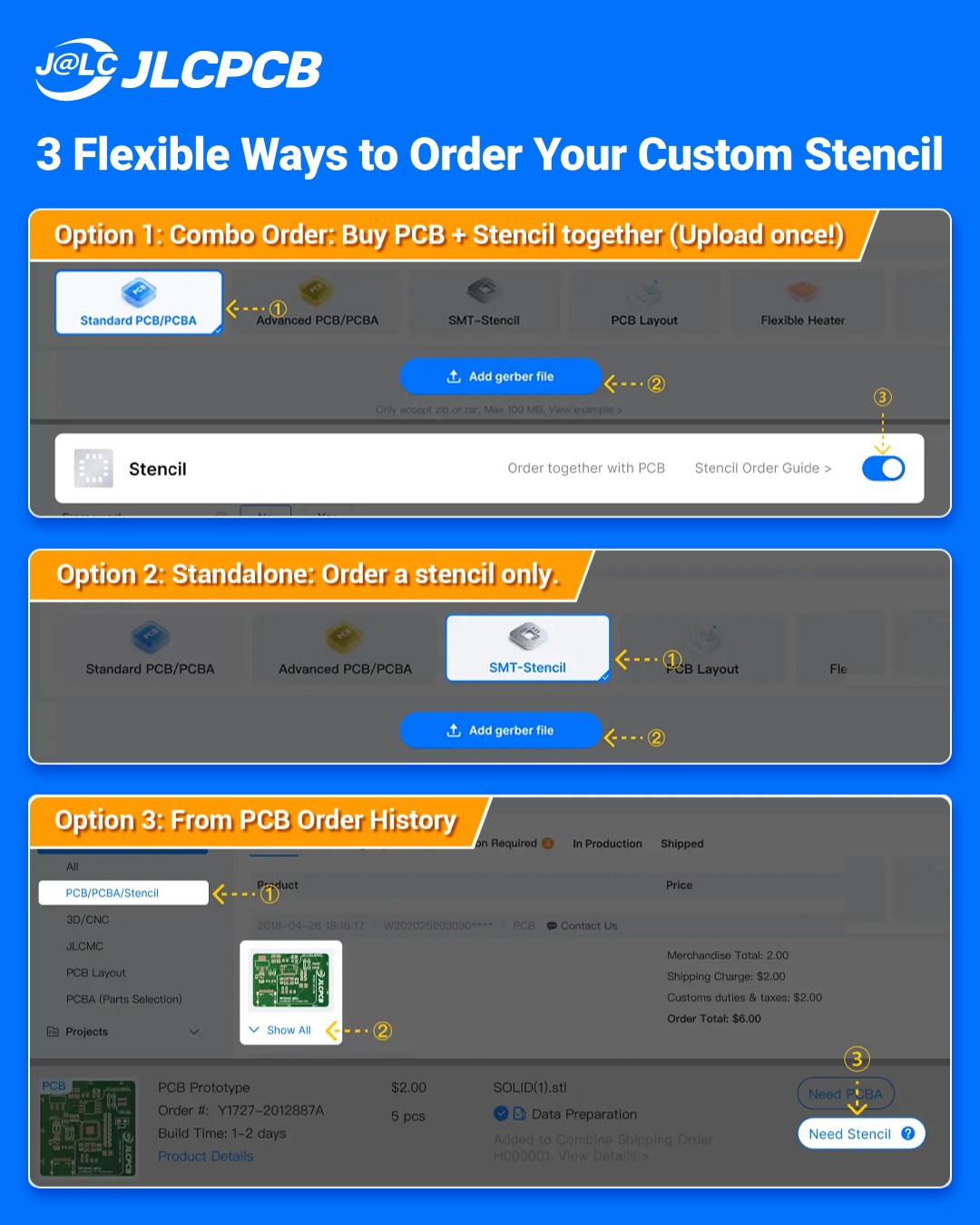
Mixed-technology designs require both a paste stencil and a glue stencil. Most industrial suppliers enforce high minimum order quantities or bundle stencils into large production lots. JLCPCB offers an MOQ of 1 piece for both stencil types, no NRE premiums, and no excess tooling sitting on a shelf while a design is still being iterated.
Paste and Glue Stencils From the Same Supplier
Both types are laser-cut from 304 HTA stainless steel, achieving ±0.003 mm precision well above the alignment requirements of any standard SMT assembly line. A single Gerber or DXF upload covers both stencil types through the same online quoting workflow: one order, one lead time, one shipping pickup.
Lead Time, Pricing, and Ordering
Starting at $3, with production as fast as 12 hours. Equally practical for a first-time hardware project and a steady small-batch production run.
Procure Precision PCB Stencils From JLCPCB
Order custom laser-cut stencils, paste, and glue from as low as $3. There is no MOQ, precision is ±0.003 mm, stainless steel 304, optionally electropolished, and optionally coated with nano-coatings. In as little as 12 hours, production is as fast as 12 hours.
Choose from Framed/Frameless, Electropolishing, Nano-coating, Step-Stencils, SMD Glue Stencil and more. Starting at $3. No MOQ. 12-Hour production.
Get $11 Coupon Now >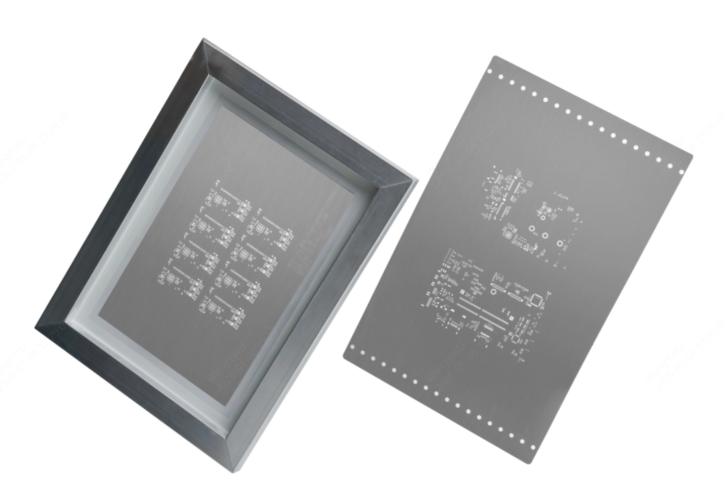
FAQs: SMD Assembly vs THT Assembly & Mixed-Tech
Can SMD components be wave-soldered without adhesive?
No. Bottom-side SMDs will immediately wash off into the 250–260°C solder pot without adhesive. To avoid this bottleneck, modern high-volume manufacturing replaces wave soldering with Through-Hole Reflow (THR), also known as Pin-in-Paste (PiP). Solder paste is printed directly into the through-holes, leaded parts are inserted, and the entire mixed-technology board passes through a standard reflow oven in a single pass — completely eliminating wave lines, adhesive stencils, and extra processing costs.
Does solder alloy selection affect stencil aperture design?
Yes, directly. Tin-lead alloys (Sn63Pb37) wet readily and allow nearly 1:1 aperture-to-pad ratios. Lead-free alloys like SAC305 require a 10–15% reduction in aperture width to prevent bridging, and electropolishing or nano-coating of the aperture walls further improves paste release.
How does IPC-A-610 define acceptable THT joint quality?
IPC-A-610 defines acceptable Through-Hole Technology (THT) solder joint quality by evaluating metallurgical bonding, wetting, and fillet geometry. An acceptable joint requires proper wetting and a smooth, continuous fillet that securely binds the component lead to the printed circuit board pad.
Conclusion: Mastering SMD Assembly vs THT Assembly with Precision Stencils
SMD assembly vs THT assembly is rarely a binary decision. In commercial electronics, the answer is almost always both.
SMD wins on density, throughput, and unit cost at volume. THT stays irreplaceable for mechanical anchoring, high-current paths, and connector roles that surface adhesion cannot sustain. Mixed-technology is the default reality, and it quietly depends on a glue-stencil step that most articles never mention.
The assembly method sets the manufacturing toolchain. The solder paste stencil or glue stencil sets the achievable yield. Getting both right is how prototype designs survive their first encounter with the production floor.
Keep Learning
The Complete Stencil Guide for Lead-Free Solder Paste Printing
Key Takeaways SAC305 is the global standard: Sn96.5/Ag3.0/Cu0.5 offers a near-eutectic melting range of 217–220°C, excellent mechanical reliability, and broad industry acceptance. SN100C (Sn-Cu-Ni+Ge) is the leading silver-free alternative for high-volume cost reduction. 34°C higher melting point shrinks process window: Lead-free alloys melt ~34°C higher than Sn63/Pb37, requiring tight reflow profiles with peak temperatures of 235–250°C and TAL of 45–90 seconds. Paste storage is non-negotiable: Store ......
SMD Assembly vs THT Assembly: A Practical Guide
Every PCB design eventually faces the same fork: should this part be SMD or THT, and what does that choice actually mean for the manufacturing line? The distinction between SMD and THT assembly extends far beyond component selection. It requires two completely separate manufacturing toolchains and introduces entirely distinct defect modes. For mixed-technology layouts, a critical intermediate step is the bottom-side adhesive process. This stage involves dispensing precise dots of thermosetting epoxy t......