
Low Df Materials: Reducing Dissipation Factor for Better High-Speed PCBs
13 min
- Understanding Dissipation Factor in PCB Materials
- How to Measure Dissipation Factor
- Impact of Dissipation Factor on PCB Performance
- Selecting Low Df Materials for Optimal Results
- JLCPCB's Expertise in Low Df PCB Manufacturing
- FAQ about Dissipation Factor
- Conclusion
Key Takeaways
Low Df materials are essential for modern high-speed PCBs as they significantly reduce dielectric loss and signal attenuation at multi-gigabit frequencies. By choosing laminates with lower dissipation factor (such as Panasonic Megtron 6, Rogers, or Isola), designers can achieve cleaner eye diagrams, support higher data rates up to 112G, and maintain better signal integrity while balancing cost through hybrid stackup strategies. Selecting the right low Df material ultimately determines whether your high-speed design passes compliance or requires expensive respins.
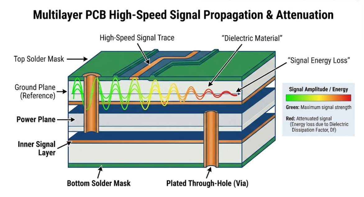
All signals passing through your PCB are silently losing energy, and it is caused by something right in the laminate itself. The higher the dissipation factor of your board material, the more of your signal's electromagnetic energy will be turned into heat as it travels through the dielectric. If it's at a low frequency, you may not hear it. However, move those data rates into multi-gigabit mode, and that little Df number that you see on the material datasheet can make the difference between clean eye diagrams and a failed compliance test.
A high dissipation factor is a big consumer of your link budget, which can result in shorter traces, equalization, or even respinning the board again. In this post, we will dive into the meaning of dissipation factor, its measurement, and why low Df materials are crucial for modern high-speed and high-frequency PCB designs. Practical material options will also be discussed, their properties will be compared, and how JLCPCB can help engineers who are working with these advanced laminates.
Understanding Dissipation Factor in PCB Materials
Before you can choose the right laminate for a high-speed design, it is important to understand what dissipation factor is, how it relates to the dielectric constant, and why it matters at high frequencies. Let's break it down.
Definition and Relationship with Dielectric Constant
The dissipation factor is also referred to as the loss tangent (tan delta) and is a measure of the amount of electromagnetic energy absorbed by a dielectric material and converted to heat as an alternating electric field is passed through it. In mathematical terms, it is the ratio of the imaginary part of the complex permittivity to the real part.
The equation is simple: Df = tan(delta) = epsilon'' / epsilon'
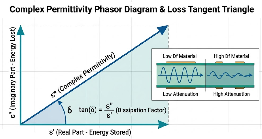
Here, epsilon' is the real part of the permittivity (which you can use to obtain the dielectric constant, Dk), and epsilon'' is the dielectric loss. The higher the Df, the more energy is lost as heat, and the less energy is propagated as a signal. Dielectric constant (Dk) and dissipation factor (Df) are closely related but have different functions. The speed of signal propagation, and the impedance of your transmission lines, is controlled by Dk. Df determines the amount of that signal that makes it through the trip. Dk is like the speed limit on a highway, and Df is the amount of fuel used in the process.
The higher the frequency, the more difficult it is for molecular polarization mechanisms in the resin system to "catch up" with the alternating field, and the more likely the dielectric losses tend to rise. Hence, a material that is acceptable at 1 GHz may be unacceptable at 10 GHz or higher.
How Dissipation Factor Affects Signal Loss in High-Frequency Designs
Signal loss in a PCB trace is due to two main factors: conductor loss (resistive loss in the copper) and dielectric loss (energy absorbed by the laminate). Conductor loss is dominant at frequencies below about 1 GHz. However, once you reach frequencies above 1-2 GHz, dielectric loss dominates and is the greatest factor in overall insertion loss.
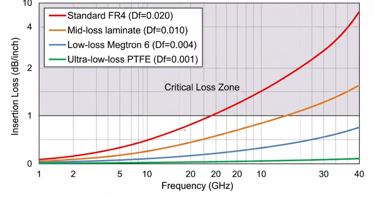
The Dielectric contribution to Insertion Loss can be approximated as:
Alpha_d (dB/inch) = 2.3 * f * sqrt(Dk) * Df / c
where (f) is the operating frequency in Hz, (D_k) is the dielectric constant, (D_f) is the dissipation factor, and (c) is the speed of light. This relation indicates that the loss of the dielectric is directly proportional to frequency and dissipation factor. From a practical point of view, it may be said that the dielectric loss per unit length doubles if the operating frequency is doubled.
How to Measure Dissipation Factor
Knowing the Df value on a datasheet is one thing. It is also important to understand how this number came about and what it actually means in terms of your design frequency.
Common Testing Methods and Standards
There are several standard ways of measuring dissipation factor, each applicable to a range of frequencies and/or accuracy.
Parallel Plate Capacitor method: This technique is based on the use of a laminate sample between two conductive electrodes as a capacitor. Then the capacitance and dielectric loss are measured, and (D_k) and (D_f) are calculated. This is a common technique used at relatively low frequencies (1MHz to 1GHz) and often mentioned in PCB material data sheets.
Stripline Resonator Method: In this method, a stripline resonator is made from the test laminate. Finally, the resonant frequency and quality factor (Q) of the structure are measured, and (D_k) and (D_f) are extracted from this. The test structure is very similar to a real PCB transmission line, so the results from this test are very representative of real-world PCB performance.
Balanced Disk Resonator Method: This method is based on the same principles as the stripline resonator technique, except that a circular disk resonator geometry is used. It provides high accuracy at microwave frequencies and is widely used for high-end RF and material characterization at high speeds.
Interpreting Df Values for Different Applications
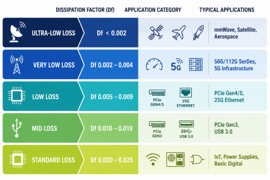
Always check the test frequency on datasheets when reading a Df value. A material listed at Df = 0.015 at 1 MHz may exhibit Df = 0.022 at 10 GHz. The frequency dependence of Df is very important and is sometimes overlooked. Here is a practical classification of Df ranges and their typical application suitability:
| Df Range (at 10 GHz) | Material Class | Typical Applications |
|---|---|---|
| 0.020 - 0.025 | Standard Loss (FR4) | Digital logic below 2 Gbps, power supplies, IoT |
| 0.010 - 0.019 | Mid Loss | PCIe Gen3, USB 3.0, SATA III, general networking |
| 0.005 - 0.009 | Low Loss | PCIe Gen4/5, 10G/25G Ethernet, DDR5 |
| 0.002 - 0.004 | Very Low Loss | 56G/112G SerDes, 5G infrastructure, radar |
| < 0.002 | Ultra-Low Loss (PTFE) | mmWave (77 GHz automotive radar), satellite, aerospace |
Impact of Dissipation Factor on PCB Performance
Signal Attenuation and Data Rate Limitations
Each high-speed serial link has a loss budget. The amplitude at which the transmitter sends a signal and the amplitude at which the receiver can detect a logic level (after equalization) are different. The channel insertion loss, which is the predominant loss at high frequencies due to the dielectric loss, defines the maximum length of the trace that can be run without losing the signal.
Here are some practical consequences:
PCIe Gen5 (32 GT/s, NRZ): Specification permits ~36 dB channel insertion loss at the Nyquist frequency (16 GHz). Even if it is a standard FR4, a 6" trace might already take up a large part of that budget, and there is not much left for connectors, vias, and package routing.
5G mmWave (28 GHz, 39 GHz): FR4 is practically not usable at these frequencies. Only PTFE-based or special low-Df ceramic-filled laminates allow acceptable performance.
As Df increases, so does the degradation of the eye diagram quality. The frequency dependence of Dielectric loss creates a low-pass filter, which makes digital signals more rounded. This adds jitter, lowers eye height and eye width, and hence restricts the ultimate Bit Error Rate (BER) that can be achieved.
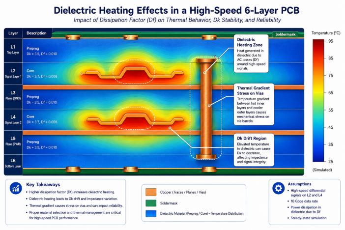
Thermal and Reliability Considerations
The energy absorbed by the dielectric is not lost. It converts to heat. For applications such as high-power RF or dense high-speed digital designs with numerous active channels, dielectric heating may be a significant contributor to the thermal load of the board.
Too much dielectric heating results in several concerns for reliability:
- Dk rises with temperature: As the laminate is heated, its Dk changes, impacting impedance and propagation delay. This results in timing uncertainties in close differential pairs and buses.
- Accelerated aging of the resin system: Increased temperatures can cause increased chemical aging of the epoxy or resin matrix, which may shorten the board's useful life.
- Thermal cycling stress: Plated through-holes and via barrels can be subjected to thermal gradients, which produce stresses, particularly in thick multilayer boards.
Most normal digital designs are dominated by thermally generated loads from the components rather than dielectric heating. However, in high-power RF boards (e.g., active antenna arrays or power amplifiers), the choice of a low-Df material is not just a signal integrity choice but a thermal management one as well.
Selecting Low Df Materials for Optimal Results
Popular Low Df Laminates and Their Properties
The market offers a wide spectrum of low-Df materials, from enhanced FR4 variants to exotic PTFE-based systems. Here is a comparison of commonly used options:
| Material | Dk (at 10 GHz) | Df (at 10 GHz) | Tg (C) | Cost Relative to FR4 | Key Applications |
|---|---|---|---|---|---|
| Standard FR4 (Tg 170) | 4.2 - 4.5 | 0.018 - 0.025 | 170 | 1x | General digital, IoT |
| Shengyi S1000-2M | 4.2 | 0.015 | 175 | 1.3x | Mid-speed digital |
| Panasonic Megtron 4 (R-5775K) | 3.8 | 0.008 | 200 | 3 - 4x | High-speed networking, PCIe Gen4 |
| Panasonic Megtron 6 (R-5775N) | 3.4 | 0.004 | 200 | 5 - 6x | 56G+ SerDes, 5G backhaul |
| Isola Astra MT77 | 3.0 | 0.0017 | 200 | 6 - 8x | mmWave, aerospace |
| Rogers RO4003C | 3.38 | 0.0027 | >280 | 8 - 10x | RF front-ends, radar |
| Rogers RO4350B | 3.48 | 0.0037 | >280 | 8 - 10x | RF power amplifiers, antennas |
| PTFE (RT/duroid 5880) | 2.2 | 0.0009 | N/A | 10 - 15x | Satellite, mmWave radar |
The trend is obvious: the lower the Df, the more expensive it is, and often more difficult to fabricate. The engineering challenge is to strike a balance between your signal integrity requirements and keeping the budget in check.
Balancing Df, Cost, and Manufacturability
In reality, many fast designs employ a hybrid stackup design and do not use an all low-Df material construction. This is how it works:
- Find out the critical signal layers: Identify the layers that have your highest-speed signals (SerDes lanes, RF traces, clock distribution).
- Use materials with low Df (Megtron 6 or similar) only where necessary, usually core and adjacent prepreg layers, for the critical signal pairs.
- Standard or mid-loss materials can be used elsewhere: Standard FR4 or mid-loss materials can be used for power planes, low-speed control signals, and mechanical support layers.
- Test for compatibility: Not all materials bond well together. Check CTE (coefficient of thermal expansion) matching, reflow compatibility, and the manufacturer's recommendations for hybrid stackup combinations.
JLCPCB's Expertise in Low Df PCB Manufacturing
Access to Premium Low Df Materials and Advanced Processes
JLCPCB has a full material library that is more than just FR4. Engineers who are designing high-speed and high-frequency projects may choose from a variety of low-Df laminates, such as the popular Shengyi, Panasonic (Megtron series), Rogers, and Isola laminates.
This material thickness is combined with cutting-edge fabrication techniques. Controlled impedance processing, laser-drilled microvia, complex HDI sequential lamination, and etching with tight tolerances are all part of the production toolkit. JLCPCB's process controls guarantee the consistency of the thickness of the dielectric and copper registration, which are both significant for the desired Dk and Df performance of the final board in RF and mmWave designs that are based on PTFE-based substrates.
Reliable Production Ensuring Consistent Signal Performance
Consistency between boards and between production lots is as critical as the material properties themselves are for high-speed channels. While a 10% change in Df may be insignificant for a general-purpose digital board, it could be the difference for a marginal 56G PAM4 channel.
Incoming material inspection, in-process impedance testing (TDR and network analyzer), and outgoing electrical verification are part of JLCPCB's quality management. Boards are made according to IPC-6012 Class 2 and Class 3 standards to guarantee that the fabricated product will meet the performance required by your design. With a quick turnaround (as fast as 1-2 days for normal builds), engineers working on prototypes can obtain physical boards in a timely manner and compare their channel simulation results to actual measured S-parameter data.
FAQ about Dissipation Factor
Q: What is the dissipation factor in a PCB?
Dissipation factor (Df), also known as loss tangent (tan delta), measures how much electromagnetic energy a PCB's dielectric material absorbs and converts to heat. It is the ratio of energy lost to energy stored per cycle in the dielectric. Lower Df values mean less signal loss, which is critical for high-speed and high-frequency designs.
Q: What is a good dissipation factor for high-speed PCBs?
For designs operating above 10 Gbps, a Df below 0.010 (at 10 GHz) is generally recommended. For very high-speed SerDes channels (56G and above), target Df below 0.005. Standard FR4 with Df around 0.020 is typically suitable only for data rates below 5 Gbps and frequencies below 2-3 GHz.
Q: How does the dissipation factor differ from the dielectric constant?
The dielectric constant (Dk) determines signal propagation speed and transmission line impedance, while the dissipation factor (Df) determines how much signal energy is lost as heat in the dielectric. Both are properties of the laminate material, and both are frequency-dependent. A high-speed design needs to control both: stable Dk for impedance accuracy and low Df for acceptable insertion loss.
Q: Can I use standard FR4 for high-frequency RF applications?
Standard FR4 is generally not suitable for RF applications above 2-3 GHz due to its relatively high Df (0.018-0.025) and poor Dk stability across frequency. For RF designs, consider materials like Rogers RO4003C (Df = 0.0027), RO4350B (Df = 0.0037), or PTFE-based laminates (Df < 0.002), depending on your frequency range.
Conclusion
One of those parameters is the dissipation factor of your PCB material. For frequencies above a few gigahertz, dielectric loss is the biggest loss mechanism, and standard FR4 simply cannot perform to the level required by modern serial protocols and RF systems. The use of a low-Df material is an engineering choice. This means knowing what frequencies you need, what stackup that correlates with, and often using a hybrid approach to achieve a balance between performance and cost. Any published Df value is as important as the number itself, and so is the measurement method and test frequency behind the number.
Keep Learning
How Modular PCB Design Simplifies Complex Electronics Projects
Key Takeaway Modular PCB design simplifies complex electronics by breaking boards into independent, reusable functional blocks with clear interfaces. It boosts reusability, speeds up debugging, enhances team collaboration, and reduces errors.Shift from flat to modular design for faster development and more scalable, reliable PCBs. Ever seen a 400+ component schematic and got your head scrambled before even beginning routing? You are not alone. With the ever-increasing density of electronics combined w......
Your Ultimate Guide to PCB Rulers
In the world of PCB design and manufacturing, having the right tools is crucial for achieving accuracy and precision. One such tool that has gained popularity among professionals and hobbyists is the PCB ruler. This specialized measuring tool is designed to provide accurate measurements, reference information, and component footprints, assisting designers, engineers, technicians, and assemblers in various stages of PCB development. In this guide, we'll explore what a PCB ruler is, the features and mea......
Understanding the Materials Used in PCBs: Selection, Types, and Importance
Key Takeaways FR-4 is the go-to material for most cost-effective and reliable PCBs. Use Rogers for high-frequency and RF applications to reduce signal loss. Higher copper weight (2oz) improves current and heat handling. Choose High-Tg substrates for better thermal stability in multilayer boards. Green LPI soldermask offers the best balance of performance and inspection. Printed circuit boards (PCBs) are an essential component of modern electronics. These boards connect and support electronic component......
How to Select Tg of PCB ?
What is the Tg of PCB? In PCB manufacturing, "Tg" stands for Glass Transition Temperature. It is the temperature at which the PCB substrate material transitions from a rigid, glassy state to a soft, rubbery state. PCBs are flame-retardant (UL94 V-0) and do not burn easily; instead, they soften above Tg. The Critical Correlation Between Tg and Z-Axis CTE (Coefficient of Thermal Expansion) When the temperature exceeds the Tg point, the PCB substrate material (such as standard FR-4) undergoes a physical ......
How to Choose the Thickness of PCB
First, In the world of electronic products, the PCB is often referred to as the "heart" of the device. It interconnects all components, making board thickness one of the most important parameters. Choosing the right PCB thickness directly affects the electrical performance, mechanical stability, thermal management, and long-term reliability of the final electronic product. The process of selecting PCB thickness is influenced by various factors, such as product application scenarios, board material, an......
PCB Copper Pour Basics
What is Copper Pour in PCB Design? Copper pour refers to the technique of filling unused areas of a PCB's copper layers with solid copper planes. These planes are connected to power or ground nets, creating a continuous conductive path. Copper pour is typically used in the power and ground planes, as well as in signal layers for specific purposes. Purpose and Benefits of Copper Pour: Copper pour is primarily used to fill unused areas on PCB copper layers with solid (or hatched) copper connected to pow......