
Achieving Reliable Signal Performance with High Frequency PCBs Through Precision Fabrication
13 min
- Selecting Materials for Superior High Frequency Performance
- Essential Design Techniques for High-Frequency PCBs
- Expert Fabrication Processes for High Frequency PCBs
- JLCPCB’s Proven Capabilities in High-Frequency PCB Delivery
- Frequently Asked Questions (FAQ)
Recently, the electronics business has continued to drive up the frequency, and that has made the previously easy PCB into an earnest RF element. Current high-frequency PCB designs are routinely operating at speeds that would have been wild 10 years ago. 5G millimeter-wave base stations are operating in the 24-40GHz band. Radar chips used in automobiles operate at 77 GHz. Wi‑Fi 7 pushes past 6 GHz, and even the so-called digital high-speed serial connections, such as PCIe Gen5 and USB 4, are transmitting signals into the multi-GHz regime.
At such gigahertz frequencies, the PCB substrate ceases to be a mere passive background. Any element of the board dielectric material, copper roughness, via geometry, trace size, and even the surface finish contributes to quantifiable loss in the signal path. Unless you consider those effects in your high-frequency PCB design, you will have a poor signal-to-noise ratio, reduced range, increased bit-error rates, and may even encounter regulatory compliance pitfalls.

There is never a higher demand for good high-frequency PCBs, and the margin of error has never been as thin as it is now. Making it right entails the selection of the right materials, working on the design, and handing over the rest to the fabrication professionals.
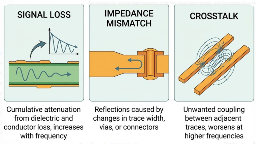
Challenges Like Signal Loss, Impedance Mismatch, and Crosstalk
Three primary challenges dominate high-frequency PCB design. Signal loss (insertion loss) is the cumulative attenuation of signal energy as it travels through the board. It comes from two sources: dielectric loss (energy absorbed by the substrate material) and conductor loss (energy dissipated as heat in the copper traces due to skin effect and surface roughness). Both increase with frequency, making material selection absolutely critical.
Impedance mismatch occurs when the characteristic impedance of a transmission line changes along its path: due to trace width variation, layer transition through vias, connector interfaces, or substrate property changes. Every mismatch creates a reflection that robs energy from the transmitted signal and can create standing waves that distort the frequency response.
Crosstalk: unwanted coupling between adjacent signal traces becomes increasingly problematic at higher frequencies because the coupling coefficient increases with frequency. What appears as adequate trace separation at 1 GHz may produce unacceptable crosstalk at 10 GHz, requiring wider spacing or shielding structures.
Selecting Materials for Superior High Frequency Performance
Low-Loss Laminates Such as Rogers, Teflon, and Hybrid Options
Standard FR-4 laminate, while perfectly adequate for digital designs up to a few hundred MHz, becomes increasingly lossy at higher frequencies. Its dissipation factor (Df) of 0.020 or higher at 10 GHz makes it unsuitable for most high-frequency PCB applications above 1-2 GHz.
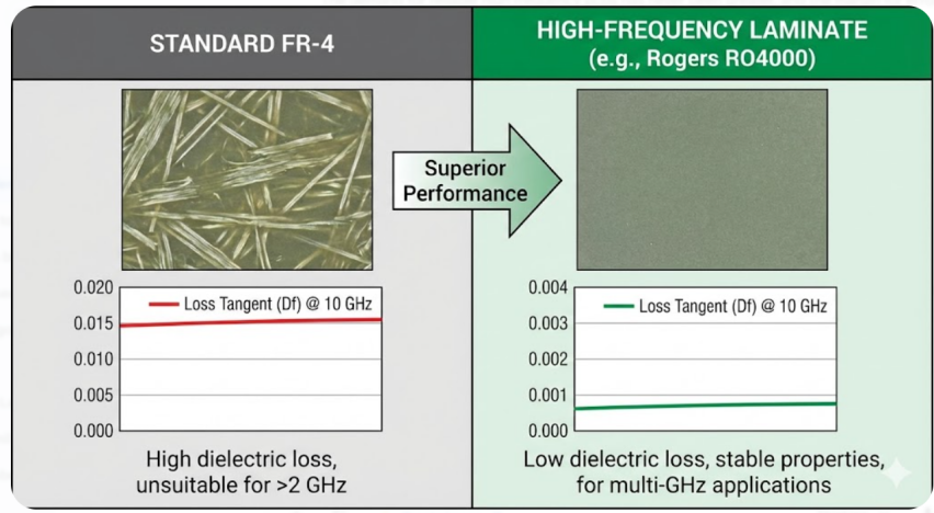
The high-frequency material landscape offers several alternatives. Rogers Corporation’s RO4000 series provides a cost-effective step up from FR-4, with Df values around 0.004 and stable dielectric properties across a wide frequency range. For more demanding applications, Rogers RO3000 series and PTFE-based laminates (often referred to as Teflon boards) offer Df values below 0.002, enabling designs well into the millimeter-wave range.
Hybrid stackups that combine high-frequency laminates on critical signal layers with standard FR-4 on non-critical layers offer a practical cost compromise. The RF signal layers get premium materials while power and low-speed control layers use economical FR-4, reducing overall board cost without sacrificing performance where it matters.
Key Properties: Dielectric Constant, Loss Tangent, and Thermal Stability
Three material properties dominate high-frequency PCB material selection. The dielectric constant (Dk or Er) determines the electrical length of traces and the characteristic impedance of transmission lines. Lower Dk values reduce trace coupling and enable tighter impedance control. Equally important is Dk stability, a material whose Dk shifts with temperature or frequency, making impedance control unpredictable.
Loss tangent (Df) is what directly informs you of the amount of dielectric loss that you are contending with. FR4 at a frequency of 10 GHz has a Df in the range of 0.020, and Rogers 4350B has a Df of around 0.0037. That would be about 5 times less loss per unit length, and that can be multiplied by the number of centimeters of trace you can run.
The problem of thermal stability is factual since most of the high-frequency systems are supposed to operate within a broad temperature range. When the Dk of a material varies significantly with temperature, changing both the insertion loss and the impedance will occur, and wipe out the performance at the temperature extremes.
Pro-tip: It is not enough to lock on the 1MHz figures on a datasheet. Get the manufacturer of the laminate to provide Dk and Df at the frequency you are actually operating at; they can change dramatically between 1MHz and 10GHz, and datasheets tend to be more optimistic than real.
Balancing Cost and Performance in Material Choices
Frankly speaking, when you use such high-frequency laminates, they are 5 to 20 times more expensive than regular FR-4 on an area basis. But you need to choose some materials that will suit the performance you require, or you will simply waste money.
Assuming that your board is not faster than 3 GHz, you can use FR4 upgraded stuff - Isola FR408HR, Panasonic Megtron 6, and the like. They are okay and significantly less expensive than the PTFE glazes. At 3 up to 15 GHz, the Rogers RO4000 line is often the compromise point in terms of performance and ease of transport. Beyond 15 GHz, you must use PTFE or ceramic-filled even at the expense of higher cost and increased effort in manufacture.
The trick is hybrid stack‑ups. You simply add those costly high-frequency layers to the areas of the board that require them, and otherwise use plain FR4. In that manner, you can save material costs by up to 40 to 60 percent and retain all the RF performance.
Essential Design Techniques for High-Frequency PCBs
Controlled Impedance Traces and Layer Stackup Planning
Every high-frequency signal trace must be designed as a controlled-impedance transmission line. This means specifying the trace width, copper thickness, dielectric thickness, and dielectric constant to achieve the target characteristic impedance (typically 50Ω for single-ended RF or 100Ω differential for high-speed digital).
High-frequency PCB stackup design begins by identifying the hot signals present on the PCB and ensuring that every one of the layers holding those signals has a solid reference plane immediately adjacent to it. The dielectric difference between the signal and reference plane freezes the impedance, therefore ensuring that it is within a narrow band of tolerance of -10 to +10%; otherwise, you will ruin the entire game.
Do not run hot lines on layers adjacent to split planes or heavily routed layers. The reference plane must have a clean and unobstructed path for the return current directly under or over the trace. Any discontinuity in that plane causes the returning current to curve around, increasing the loop area and radiating.
Via Management and Ground Plane Strategies
Vias introduce the largest cause of impedance hiccups on a high-frequency path. The via barrel is a parasitic inductor, and the antipad, a small hole in the reference plane, is a parasitic capacitor. Make the via stub short, back-drilled, or blind vias when you are pressing beyond 5GHz. The stitching of signal vias around stitch ground vias is a savior. The planes above and below are connected to a ring of ground vias to provide what appears as a coaxial-like shield that maintains the impedance constant when the signal passes between layers.
It is all about ground plane integrity. Even a tiny slot, cut, or aperture along a high-frequency trace becomes a bogus slot antenna that radiates. In case you need to squeeze a trace between a cut, drop stitching capacitors, or vias directly adjacent to that crossing to provide the return current.
Minimizing Reflections and Ensuring Signal Integrity
Reflections occur at all the points of impedance variation, trace width variations, via jumps, connector launches, component pads, whatever. You need to have a constant impedance between source and load in order to keep reflections to a minimum. A tapered transition ( consider connector footprints ) is used when you have to change the trace width. And put slap ground vias and stitching wherever you cross a layer.
Have appropriate ground structures, such as a coplanar waveguide or a grounded coplanar, designed to launch the connector, to maintain the impedance between the connector and the board clean. And 2D cross-section tools (pre-layout simulators) of impedance and 3D EM simulators (via transitions and connector launches) are imperative when operating above 5 GHz. Hiding flaws that a schematic will not reveal is the reason behind these sims, and it is much cheaper to debug them in a simulator than to go searching on a breadboard.
Expert Fabrication Processes for High Frequency PCBs
Precision Drilling, Plating, and Etching for Fine Features
The high-frequency PCB manufacturing is a real pain since you need to maintain the process tolerances tightly, unlike the normal boards. I mean trace width tolerances that remain in the range of ±0.5 mil in order to maintain the impedance at its proper spec value. It will require a precise etching of the spot, with a narrow band of control in terms of chemistry, temperature, and conveyor speed.
Accuracy in drilling is of primary concern in ensuring that vias in proximity to pads are accurate and that the appropriate amount of back-drill depth is pulled. Back-drilling by removing the unused portion of a via barrel in order to kill the stub has to strike depth accuracy of within 4mils, and you can kill the stub entirely without accidentally drilling the signal layer you are protecting.
Both in the surface copper and in the vias, plating uniformity influences control of impedance and insertion loss. Unless the plating is smooth, you form local impedance bumps and cause unneeded conductor loss as the surface becomes rougher than it ought to be.
Tight Tolerances in Registration and Surface Finish Application:
On high-frequency boards, layer-to-layer registration must be razor sharp since any displacement of reference planes will alter the effective impedance of signal lines that overlay them. High frequency designs require a registration tolerance of 2mils or better.
Surface finish is also important to high-frequency performance. ENIG provides you with a really smooth, flat surface that is good with tiny RF components, but the nickel layer can add magnetic losses at very high frequencies. High-frequency Immersion silver is magnificent since it has little additional loss. OSP is the least-lossiest one out there, but it does not last forever, so you have to trade RF performance with the storage period of boards and the manner in which they will be assembled.
Advanced Testing for Impedance and Insertion Loss Verification
All high-frequency boards need to undergo impedance testing by Time Domain Reflectometry (TDR) of test coupons embedded in the panel. TDR tests that the actual impedance matches the design one within the tolerance we are seeking to achieve, say ±10 percent or even ±5 percent in the most challenging cases.
To verify that your critical RF designs are working, you will also make measurements of insertion loss on test structures to verify that the material mix, copper roughness, and fabrication steps are all yielding the signal performance you desire. These measurements provide you with the real and objective data that cannot be substituted through a simulation. A good manufacturer of high-frequency PCB will provide the test information with the end-quality documentation.
JLCPCB’s Proven Capabilities in High-Frequency PCB Delivery
Access to Premium Materials and State-of-the-Art Equipment
JLCPCB has the best laminate suppliers, such as Rogers, thus we will be able to grab a handful of high-frequency materials that will not cost us an arm and a leg. Combine that with high-quality gearing that drives to the tight fit high-frequency designers require, and JLCPCB takes care of most of it, whether it is quick prototyping or full production.
Specialized DFM Support for High Frequency Designs
DFM early collaboration is truly worthwhile, particularly when you are new to high-frequency work. The engineering team at JLCPCB will give a glance at your stack-up, material selection, and impedance requests and point out any possible hiccups, not to mention throwing in optimization hints, prior to you entering prod. This active assistance is highly appreciated by any person who is going to work on the high-frequency design in the initial stage.
Reliable Production from Prototypes to High-Volume Runs

You can get high-frequency performance at every volume, whether you are assembling five prototype boards to test your 5G antenna or ordering five thousand panels for a radar module; JLCPCB keeps the high-frequency performance consistent at all volumes. The same process regards material specifications and quality checks at any scale, and hence, the prototype tested design would be equally effective in mass production.

Frequently Asked Questions (FAQ)
What makes a PCB a high-frequency PCB?
A high-frequency PCB is designed specifically for signals operating above approximately 1 GHz, using specialized low-loss laminate materials, controlled-impedance transmission lines, and precision fabrication processes to minimize signal degradation. The exact frequency threshold depends on the application’s performance requirements.
Can I use FR-4 for high-frequency applications?
Standard FR-4 is generally suitable up to about 1-2 GHz for non-critical applications. Above that, its high dielectric loss degrades signal quality rapidly. Enhanced FR-4 variants can extend this range to about 3-5 GHz. Above 5 GHz, dedicated high-frequency laminates like Rogers or PTFE-based materials are typically necessary.
How much does high-frequency PCB fabrication cost compared to standard boards?
High-frequency boards typically cost 2- 5x more than standard FR-4 boards of similar complexity, primarily due to premium laminate materials. Hybrid stackups (mixing high-frequency and standard materials) can reduce this premium by 40-60% while maintaining RF performance on critical layers.
What is the most important factor for high-frequency PCB performance?
Material selection (specifically loss tangent) has the single largest impact on signal performance. However, a premium laminate processed with poor fabrication tolerances will underperform a mid-range laminate fabricated with precision. Both material and fabrication quality must be excellent for optimal results.
Do I need back-drilling for my high-frequency design?
Back-drilling becomes important for through-hole vias carrying signals above approximately 5GHz, where the via stub creates a significant impedance discontinuity and resonance. For lower frequencies or designs using blind/buried vias (which inherently have no stub), back-drilling is unnecessary.
Keep Learning
Building Reliable High-Speed Performance with Effective Timing Analysis
Key Takeaways Timing analysis is essential for high-speed PCBs — clean signals can still fail if they miss setup or hold windows. Focus on setup time, hold time, clock skew, and propagation delay to ensure reliable data sampling. Prioritize length matching, controlled impedance, and proper stackup to maintain positive timing margins. Combine static timing analysis with dynamic simulation for best results. Precision manufacturing is critical — small variations in impedance or dielectric thickness can d......
Low Loss PCBs : Advanced Materials for Superior High-Speed Signal Performance
Key Takeaways Low Loss PCBs using advanced materials like Rogers RO4003C, RO4350B, and PTFE laminates deliver superior signal integrity by dramatically reducing dielectric loss at multi-gigahertz frequencies. Ideal for 5G, mmWave, RF, and high-speed digital designs, these boards offer significantly lower insertion loss, stable impedance, and better thermal performance compared to standard FR4. By choosing the right low-loss laminate and partnering with experienced manufacturers like JLCPCB, engineers ......
How to Reduce Insertion Loss for Better High-Speed PCB Performance
Key Takeaways Reducing insertion loss is essential for achieving reliable high-speed PCB performance. By selecting low-loss materials with lower Df, optimizing trace routing and stackup design, minimizing via transitions, using smoother copper foils, and applying precision manufacturing techniques, designers can significantly lower both dielectric and conductor losses. These strategies help maintain better signal integrity, wider eye openings, and higher data rates in multi-gigabit designs. Have you e......
How to Create the Perfect PCB Stackup for High-Speed and Reliable Designs
Key Takeaways A well-designed PCB stackup is the foundation of high-speed, reliable designs, determining signal integrity, controlled impedance, and EMI performance. Use symmetrical layers with adjacent reference planes, proper dielectric spacing, and copper balancing to avoid warpage and crosstalk. Choose standard FR4 for <3 GHz or low-loss materials (Megtron 6, Rogers) for higher speeds, and work closely with manufacturers for optimal results. Mastering your stackup is essential for high-speed succe......
Achieving Reliable High-Speed Performance with PCB Transmission Lines
Key Takeaways PCB Transmission Lines are essential for reliable high-speed PCB performance in USB 3.0, PCIe, DDR4, and RF designs, turning traces into controlled-impedance structures that eliminate reflections, crosstalk, and attenuation. Select microstrip, stripline, or GCPW geometries with accurate calculations, continuous reference planes, mitered bends, and 3W spacing, then rely on precise etching, copper profile control, and TDR testing at JLCPCB for consistent results from prototype to volume pr......
Backdrill Vias: Enhancing Signal Integrity in High-Speed PCBs
Key Takeaways Backdrill vias remove unused copper stubs from plated through-hole vias, shortening the residual stub to under 0.15 mm (6 mils). This eliminates impedance discontinuities, reflections, and resonances in high-speed signals above 5–10 Gbps. It delivers better return loss, insertion loss, lower jitter, and clearer eye diagrams — all while keeping simple stack-ups and far lower cost than blind/buried vias. Use backdrilling for any stub longer than 15 mils (0.381 mm), especially on boards thi......