
PCB Design : How to Resolve Short Circuit Defects Caused by HASL
9 min
- Introduction
- Understanding the HASL Process and Why Short Circuits Occur
- Why ENIG is the Recommended Solution for Dense Designs
- Detailed Comparison: HASL vs. ENIG at JLCPCB
- Practical PCB Design Recommendations to Minimize Risks
- FAQ about Short Circuit Defects Caused by HASL
- Conclusion and Actionable Advice
Key Takeaways
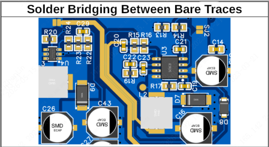
In high-density PCB designs, HASL frequently causes solder bridging and short circuits due to its uneven surface and molten solder flow, especially on fine-pitch and dense traces. The most effective solution is to switch to ENIG (Electroless Nickel Immersion Gold), which provides superior planarity, significantly reduces bridging risks, and improves assembly yield. By selecting ENIG for dense layouts, optimizing solder mask design, and running DFM checks, designers can effectively eliminate HASL-related defects while achieving higher reliability at JLCPCB.
Introduction
In modern high-density PCB designs, short circuits caused by surface finish processes remain a frequent challenge during manufacturing and assembly. Hot Air Solder Leveling (HASL) is still one of the most economical surface finishes offered by JLCPCB. However, for boards with dense traces, fine-pitch components, or coil patterns, HASL can easily cause solder bridging and short circuits. This article provides a comprehensive analysis of the root causes and recommends effective solutions, focusing on Electroless Nickel Immersion Gold (ENIG), fully aligned with JLCPCB’s actual manufacturing capabilities.
Understanding the HASL Process and Why Short Circuits Occur
HASL Process Steps (JLCPCB Implementation)
HASL, also known as Hot Air Solder Leveling, is a traditional surface finish method. The bare PCB, after etching and solder mask application, is first cleaned and fluxed. It is then dipped vertically into a molten solder bath (leaded SnPb or lead-free SnAgCu alloy). As the board is withdrawn, high-pressure hot air knives level the excess molten solder, leaving a thin coating on exposed copper pads and traces.
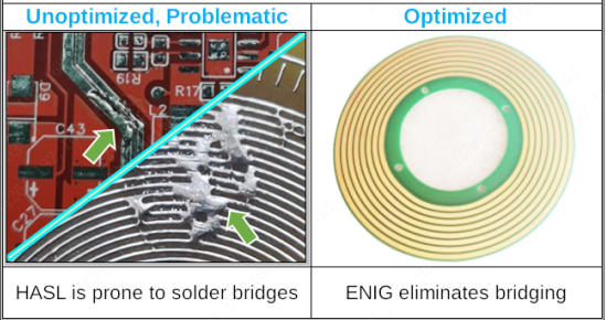
While this process is reliable and cost-effective for standard designs, it presents significant challenges in high-density layouts. The molten solder has high surface tension and fluidity. In regions with narrow solder mask openings or closely spaced traces, it tends to adhere to adjacent copper features before solidifying, forming unwanted bridges that result in short circuits.
Common Scenarios Prone to HASL Bridging
- Dense SMD pads with pitch ≤ 0.5 mm (e.g., QFN, BGA, 0201 components)
- Coil boards or RF circuits with numerous parallel fine traces
- Areas with small “window openings” in solder mask where clearance is insufficient
- Multi-layer or HDI boards with varying thermal mass
Production experience and JLCPCB guidelines show that these issues become prominent when trace spacing approaches the practical limits for uniform solder distribution.
Root Technical Causes
The primary reasons stem from the inherent characteristics of the HASL process. The resulting surface is non-planar, with solder thickness varying significantly (approximately 5–50 μm), creating peaks and valleys. During hot air leveling, excess solder can migrate laterally in dense regions. Narrow solder mask dams or insufficient clearance allow molten solder to wet unintended areas. Variations in board thickness, copper weight, and preheat conditions can further worsen bridging. These factors ultimately lead to higher defect rates in SMT assembly, increased rework costs, and reduced yield.
Why ENIG is the Recommended Solution for Dense Designs
ENIG Process Overview and Advantages
ENIG (Electroless Nickel / Immersion Gold) uses a chemical plating process that deposits a nickel barrier layer (typically 3–6 μm thick) followed by a thin gold layer (0.05–0.2 μm). This creates a mirror-flat, highly uniform surface. Unlike HASL’s physical leveling, ENIG completely avoids solder flow variability. JLCPCB offers ENIG as a standard option for most board types, including 6+ layer boards and RF applications.
Key Benefits for Short Circuit Prevention
- Superior planarity that virtually eliminates bridging risks even at fine pitches below 0.5 mm
- Consistent thickness with no peaks or valleys that trap or redirect solder during reflow
- Excellent compatibility with high-density interconnects (HDI), coil patterns, and dense mask openings
- Longer shelf life and strong oxidation resistance, ideal for humid environments
- Full RoHS compliance as it is chemically lead-free
While ENIG has a higher cost than HASL, the investment is often offset by significantly improved first-pass yield and fewer assembly defects.
Detailed Comparison: HASL vs. ENIG at JLCPCB
Overview of HASL and ENIG
HASL and ENIG represent two fundamentally different approaches to PCB surface finishing. HASL relies on a physical process (molten solder dipping + hot air leveling), while ENIG uses a chemical deposition method. This difference directly impacts surface flatness, bridging risk, cost, and suitability for dense designs. Understanding these trade-offs helps designers make informed decisions to avoid short circuit defects.
Performance Metrics Table (Based on JLCPCB Data)
| Feature | HASL / Lead-free HASL | ENIG (Immersion Gold) | Best Use Case Recommendation |
|---|---|---|---|
| Cost | Lowest | Moderate to Higher | HASL for simple; ENIG for dense |
| Surface Flatness | Uneven (prone to bridging) | Excellent (planar) | ENIG for fine-pitch |
| Fine Pitch Compatibility | Limited (≥ 0.5 mm recommended) | Excellent (< 0.5 mm, down to 0.3 mm+) | ENIG |
| Solderability | Good (but variable) | Excellent & consistent | ENIG |
| Shelf Life | 6–12 months | >12 months | ENIG |
| RoHS Compliance | Lead-free version available | Fully compliant | ENIG |
| Typical Thickness | Variable (5–50+ μm) | Ni: 3–6 μm, Au: 0.05–0.2 μm | - |
| Applications | Through-hole, low-density, prototypes | HDI, BGA/QFN, coil/RF, high-reliability | See design section |
This comparison clearly shows when to choose each finish. HASL suits cost-sensitive, coarse-pitch boards, while ENIG excels in dense and high-reliability designs.
In-Depth Analysis of Key Differences
HASL remains the most cost-effective choice for many standard applications. Its pre-tinned surface offers excellent initial solderability, making it suitable for through-hole and coarser-pitch SMD components. However, the uneven topography created by the hot air leveling process increases the risk of solder bridging in dense areas — precisely the short circuit issue this article addresses.
In contrast, ENIG provides a flat, uniform surface that significantly reduces bridging risks and improves assembly yield for fine-pitch components such as BGAs, QFNs, and 0201 packages. The nickel barrier layer also prevents copper diffusion, while the thin gold layer offers superior corrosion resistance and longer shelf life. Although ENIG costs more due to the precious metals and additional chemical steps, it is often the more economical choice overall for high-density or high-reliability boards because it minimizes defects and rework.
Practical PCB Design Recommendations to Minimize Risks
Surface Finish Selection Strategy
Evaluate your design’s minimum pitch and density early in the layout stage. In the JLCPCB ordering interface, select ENIG for any board containing features prone to HASL bridging. Always run the free online DFM analysis on your Gerber files before submission to catch potential issues.
Solder Mask and Clearance Optimization
- Maintain adequate solder mask dam width (minimum ~0.1 mm depending on process)
- Follow JLCPCB’s recommended solder mask expansion (typically 0.05–0.1 mm)
- Consider Non-Solder Mask Defined (NSMD) pads in dense areas
- Slightly increase trace-to-trace spacing in critical zones if HASL must be used
Trace Spacing and Layout Best Practices
Follow JLCPCB’s minimum trace/space rules based on copper weight and layer count. Adding teardrops on pads improves reliability. For coil and RF sections, route critical signals on inner layers with proper ground plane shielding. Perform thorough DRC and consider thermal profile simulation for reflow assembly.
Additional Manufacturing and Assembly Tips
- Use proper panelization with appropriate array spacing and fiducials for better SMT handling
- For ENIG boards, standard stencil thickness (0.1–0.12 mm) usually works well due to excellent flatness
- Order Flying Probe or fixture electrical testing to detect latent shorts early
- Start with small prototype runs to validate the surface finish choice before scaling to volume production
FAQ about Short Circuit Defects Caused by HASL
Q: What is the main cause of short circuits when using HASL?
The main cause is the uneven, non-planar solder surface created during vertical immersion and hot air leveling. In dense areas or with fine pitches, molten solder easily bridges adjacent traces or pads before it solidifies.
Q: When should I choose ENIG instead of HASL at JLCPCB?
Choose ENIG when your design has trace spacing or component pitch ≤ 0.5 mm, dense SMD pads, coil/RF patterns, BGA/QFN packages, or when you need high assembly yield and reliability. For simple, low-density, or cost-sensitive boards with pitch > 0.65 mm, HASL is usually sufficient.
Q: How much more expensive is ENIG compared to HASL?
ENIG is moderately more expensive than HASL or Lead-free HASL, but the price difference at JLCPCB is reasonable and often offset by reduced defects and rework. Check the real-time quote in the JLCPCB ordering system for your specific board parameters.
Q: Does switching to ENIG affect signal integrity or impedance control?
ENIG has excellent planarity and minimal impact on impedance. Its thin, uniform coating (Ni + Au) is well-suited for high-frequency and RF boards. It is often preferred over HASL for impedance-critical designs because of its consistency.
Q: Can I still use HASL safely for dense designs?
It is possible but risky. You would need to increase trace spacing, enlarge solder mask openings carefully, and accept potentially lower yield. For most dense or fine-pitch boards, JLCPCB recommends ENIG to avoid bridging issues.
Q:How do I specify the surface finish when ordering at JLCPCB?
In the JLCPCB online order page, simply select “ENIG” or “Immersion Gold” under Surface Finish options. Upload your Gerber files and run the DFM check — the system will flag potential issues. You can also add notes in the order comments if needed.
Conclusion and Actionable Advice
Switching from HASL to ENIG for dense-circuit or fine-feature PCBs is one of the most effective ways to resolve short circuit defects caused by solder adhesion. JLCPCB makes this transition easy with clear options, competitive pricing, and robust DFM support. By combining the right surface finish with good layout practices, you can significantly improve manufacturing yield, reduce assembly defects, and enhance overall product reliability.
Keep Learning
Why Tolerance Analysis Is Key to Reliable and Cost-Effective PCB Production
Key Takeaways Tolerance analysis bridges CAD perfection and manufacturing variations to ensure reliable PCB assembly. Focus on critical areas: annular rings, hole tolerances, trace/space, layer registration, and solder mask alignment. Apply Worst-Case, RSS, or Monte Carlo methods for effective tolerance stack-up. Proper analysis boosts yield, cuts respins and costs — start with JLCPCB’s DFM review. Have you ever sent a board to fabrication, which appeared flawless on the computer screen, but then foun......
The Ultimate Guide to PCB Panelization: Tools and Techniques
Printed circuit boards (PCBs) are the backbone of modern electronics. One critical aspect of PCB manufacturing is panelization — the process of arranging multiple PCBs onto a single larger panel for efficient manufacturing and assembly. This technique allows multiple boards to be processed simultaneously, significantly reducing costs and improving production efficiency. In this article, we will provide a comprehensive guide to PCB panelization, covering the tools and techniques required for successful......
Castellated PCBs: Introduction and Design Requirements
With the rapid development of electronic technology, electronic products are moving towards miniaturization, portability, multi-functionality, high integration, and high reliability.Consequently, printed circuit boards (PCBs) are frequently designed to integrate pre-existing, off-the-shelf modules. For example, IoT Bluetooth modules or NB-IoT modules, which are indispensable communication modules, can be soldered onto PCBs just like chips. These carrier boards are characterized by their small size and......
Copper Balancing in PCBs: Achieving Optimal Performance and High Yields with JLCPCB
Key Takeaways Copper balancing strategically distributes copper across PCB layers to create uniform density, preventing warpage, uneven plating, inconsistent etching, and signal integrity issues. The ideal copper density target sits within the 40%–60% golden ratio, with mirrored layers maintaining density variation within 15%–20% per IPC-6012 standards. Copper thieving (dot patterns or crosshatch meshes) equalizes current density during electroplating without introducing parasitic capacitance on spars......
PCB Design : How to Resolve Short Circuit Defects Caused by HASL
Key Takeaways In high-density PCB designs, HASL frequently causes solder bridging and short circuits due to its uneven surface and molten solder flow, especially on fine-pitch and dense traces. The most effective solution is to switch to ENIG (Electroless Nickel Immersion Gold), which provides superior planarity, significantly reduces bridging risks, and improves assembly yield. By selecting ENIG for dense layouts, optimizing solder mask design, and running DFM checks, designers can effectively elimin......
Design Process of a Surface Mount PCB
Key Takeaways Mastering the surface mount PCB design process is essential for creating compact, high-density, and reliable electronic boards. This comprehensive guide walks through the complete SMT workflow — from schematic capture and component selection to optimized layout, precise routing, DRC/ERC verification, and Gerber file generation — enabling designers to achieve superior performance, better manufacturability, and cost efficiency compared to traditional through-hole methods. By following thes......