Ground Symbols Explained: Earth, Chassis, Signal, Analog, Digital Ground & More
19 min
- Ground Symbol Chart (Quick Reference)
- What Is a Ground Symbol?
- Earth Ground Symbol (IEC 60417-5017)
- Protective Earth Symbol (IEC 60417-5019)
- Chassis/Frame Ground Symbol (IEC 60417-5020)
- Signal Ground Symbol (IEEE 315)
- Functional Earth Symbol (IEC 60417-5018)
- Analog, Digital, and Power Ground Symbols (AGND, DGND, PGND)
- Earth Ground vs Chassis Ground vs Signal Ground: Symbols Comparison
- IEC 60417 vs IEEE 315 Ground Symbols
- Ground Symbols in KiCad, Altium Designer, and EasyEDA
- How to Read Ground Symbols in a Circuit Diagram
- From Ground Symbol to PCB Ground Plane
- Conclusion
- FAQs About Ground Symbols

Key Takeaways
⬇ Download the Ground Symbol Cheat Sheet (PDF)
Keep all six ground symbols and their standard numbers on one page for quick reference.
- Four IEC 60417 symbols: IEC 60417 defines symbol 5017 for earth, 5018 for functional earth, 5019 for protective earth, and 5020 for frame/chassis.
- Protective earth is safety-related: IEC 60417-5019 identifies the protective earth connection and is used for safety-related protective bonding.
- Signal ground uses a different convention: IEEE Std 315 defines the signal-ground symbol and its labeled variants for circuit reference points.
- Chassis is not necessarily earth: A chassis or frame can be at a different electrical potential from earth and should not automatically be treated as an earth connection.
The ground symbol is probably the most familiar mark on any schematic, so it is easy to assume that all ground symbols mean the same thing. But in reality, they don't.
Earth, protective earth, chassis, and signal ground serve different purposes. Confusing them can range from signal integrity issues, such as ground loops, voltage offsets, and EMI, to safety hazards like an inadequately grounded enclosure. Understanding what each symbol actually specifies is the first step to avoiding both.
In this guide, you will learn:
- Types of ground symbols: Earth, protective earth, chassis, and signal
- Why earth, chassis, and signal grounds use different symbols
- How to tell analog, digital, and power ground apart on a schematic
- Which ground symbol safety rules actually require you to use
- How schematic ground symbols map to PCB nets, planes, and stitching connections
Ground Symbol Chart (Quick Reference)
Six ground symbols cover almost every schematic and equipment label you will meet. Four of them are numbered in IEC 60417, and the last two come from IEEE 315. The following chart separates them at a glance.
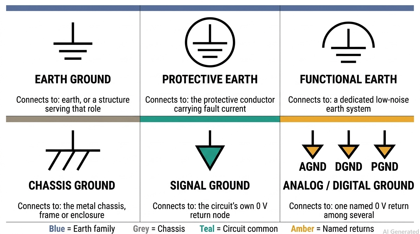
Figure: A labeled quick-reference chart showing all six ground symbols
Ground Symbol Chart: All Six Symbols Compared
| Symbol Drawn | Ground Type | Standard Reference | What It Connects To | Where You See It |
|---|---|---|---|---|
| Three bars, each shorter than the last | Earth ground, general | IEC 60417-5017; IEEE 315 clause 3.9.1 | Earth, or a structure serving that role | Mains gear, generic ground on schematics |
| The earth mark inside a circle | Protective earth (PE) | IEC 60417-5019; IEEE 315 clause 3.9.1.2 | The protective conductor carrying fault current | Earth studs, terminal blocks, Class I enclosures |
| The earthmarks under a semicircular arc | Functional, or noiseless, earth | IEC 60417-5018; IEEE 315 clause 3.9.1.1 | A dedicated low-noise earth system | Instruments, screened rooms, telecom racks |
| One bar with three angled strokes below | Chassis or frame ground | IEC 60417-5020; IEEE 315 clause 3.9.2 | The metal chassis, frame or enclosure | Automotive, RF shields, rack equipment |
| A solid or hollow triangle | Signal, or common, ground | IEEE 315 clause 3.9.3 | The circuit's own 0 V return node | Almost every electronics schematic |
| A triangle labeled AGND, DGND or PGND | Analog, digital or power ground | IEEE 315 clause 3.9.3 lettering | One named 0 V return among several | Mixed-signal, converter and motor-drive boards |
What Is a Ground Symbol?
A ground symbol marks the node a circuit treats as its zero-volt reference. For signal ground, this node typically also serves as the current return path; for protective and earth grounds, it does not carry current under normal operation.
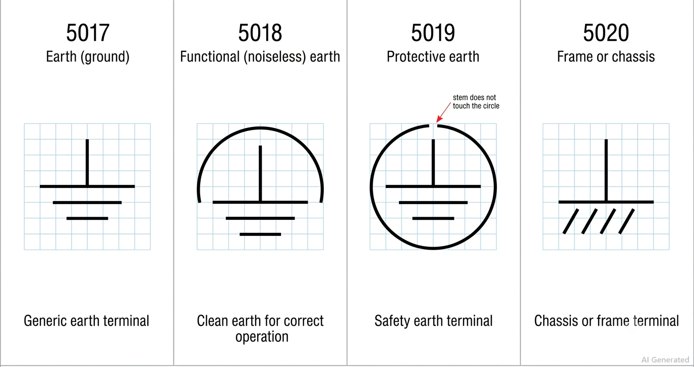
Figure: The four IEC 60417 earth and chassis symbols, 5017, 5018, 5019 and 5020
A ground symbol can communicate four things at once:
- Reference: It can define the reference point against which circuit voltages are measured.
- Return: It can provide a return path for current flowing through the circuit.
- Connection: In a schematic, matching ground symbols can indicate the same electrical net without a wire drawn between them.
- Declaration: A protective-earth symbol communicates a safety-related connection, not simply a drafting preference.
That fourth role is why ground symbols are not interchangeable. The first three describe electrical behavior—reference, return, and connectivity. The fourth communicates what the connection means for the physical hardware and, in the case of protective earth, for safety.
Earth Ground Symbol (IEC 60417-5017)
The earth ground symbol is a vertical stem meeting three horizontal bars that shorten as they descend.
IEC 60417-5017 identifies an earth terminal or connection and is distinct from the symbols for protective earth and functional earth.
IEEE Std 315, Clause 3.9.1, defines this graphical convention as a general ground symbol and gives it a broader scope than the IEC earth symbol alone might suggest.
It covers two distinct cases:
- A direct conducting connection to the earth, or to a body of water forming part of it.
- A conducting connection to a structure serving a similar function, such as an air, space, or land vehicle frame that is not conductively connected to earth.
Read that second case again, because it is the one that surprises people. An aircraft in flight has no connection to the planet at all, yet its airframe is a legitimate 5017 ground under IEEE 315. The symbol describes the role the conductor plays, not its altitude.
How to Draw the Earth Ground Symbol Correctly
Three details separate a correct 5017 from a sloppy one.
- Three bars, centered on the stem, each shorter than the one above it.
- The vertical stem terminates at the center of the top bar.
- Do not add a circle, arc, or other graphical elements; these can change the symbol's meaning or turn it into a different standardized symbol.
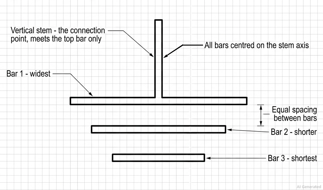
Figure: The earth ground symbol
Note
IEC 60417-5017 is the earth symbol. When the connection is intended for protective purposes, IEC 60417-5019 is used instead. When the earth connection is provided for functional purposes rather than primarily for protection against electric shock, IEC 60417-5018 is used.
Protective Earth Symbol (IEC 60417-5019)
The protective earth symbol is the earth symbol enclosed within a circle.
IEC 60417-5019 identifies a terminal intended for connection to an external protective conductor, which provides a path for fault current and helps ensure automatic disconnection in the event of a fault.
Unlike the other ground symbols in this guide, this one has a direct safety and regulatory meaning. It is not simply describing how the circuit works; it identifies a safety-related connection whose implementation can be verified during safety testing or inspection.
Protective Earth Symbol Marking Rules (IEC 60204-1)
IEC 60204-1 clause 8.2.6 governs how a protective conductor connection point is marked and names the graphic symbol first.
| Marking Method | What It Looks Like | Status Under Clause 8.2.6 |
|---|---|---|
| Graphic symbol IEC 60417-5019 | The earth mark inside a circle | Accepted, and stated as preferred |
| Letters PE | "PE" marked at the terminal | Accepted |
| Bicolor green-and-yellow | Green-and-yellow sleeve, label or insulation | Accepted |
| Any combination of these | Symbol plus letters plus colour | Accepted |
In the standard drawing, the vertical stem stops short of the circle and never touches it. That one detail is the most widely copied error in the industry, and the mistakes section below shows where it started.
This marking can be found on protective-earth terminal blocks, earthing tabs, grounding lugs, and other protective-conductor connection points. You can also browse relevant components in the JLCPCB Parts Library.
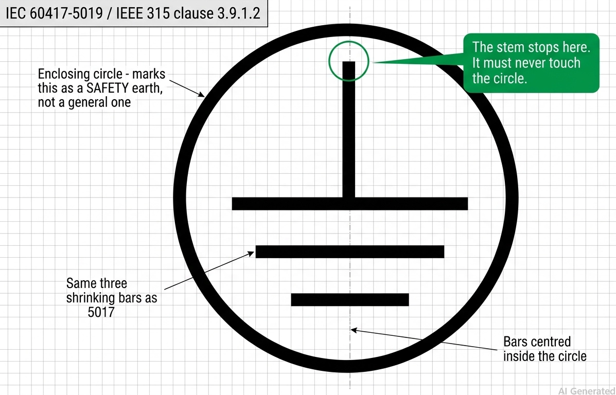
Figure: The protective earth symbol
Note
A protective-earth connection provides a fault-current path that supports operation of the protective device and automatic disconnection during a fault. For the protection-device side of the circuit, see our guide to fuse symbols.
Chassis/Frame Ground Symbol (IEC 60417-5020)
The chassis ground symbol is a single horizontal bar with three short strokes angled beneath it. IEC 60417-5020 is titled "Frame or chassis" and identifies the frame or chassis terminal.
IEEE Std 315, Clause 3.9.2, also uses this graphical convention for an equivalent chassis connection on a printed-wiring board and notes that the chassis or frame may be at substantial potential with respect to the earth or structure around it.
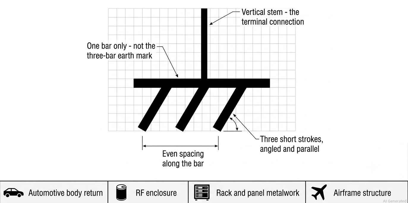
Figure: The chassis ground symbol
Note
IEEE 315 clause 3.9.2 states the chassis or frame may be at substantial potential with respect to the earth or structure it is mounted in. A chassis symbol does not imply that the node is at earth potential.
Where the Chassis Ground Symbol Is Used
- Automotive: the vehicle body or chassis is often used as a common return path for parts of the electrical system.
- RF and microwave: shield cans, connector shells, and cavity walls are commonly bonded to the chassis to control shielding and return-current paths.
- Rack and panel equipment: the metal chassis or rack structure that a card cage or PCB assembly mounts to.
- Aerospace: the airframe can serve as a common electrical structure or return path for parts of the system.
Whether that chassis is also earth is a separate decision you have to make. In a Class I product, the chassis is bonded to protective earth through a defined conductor. Leave that bond implied and two things go wrong. The assembler has no instruction to fit the strap, and the reviewer cannot tell whether the metalwork is earthed or floating.
Signal Ground Symbol (IEEE 315)
The signal ground symbol is a triangular graphical symbol used to identify a common or signal reference connection.
IEEE Std 315, Clause 3.9.3, defines the symbol as a common connection; points marked with the same designation are treated as electrically common in the schematic. The clause also specifies how the symbol can be labeled with an identifying value, letter, number, or other mark.
Signal Ground Symbol Variants
| Symbol / Variant | Meaning | Example |
|---|---|---|
| Solid-filled triangle | Circuit common, the 0 V return | GND |
| Hollow outline triangle | Same function, a drafting-office preference | GND |
| Triangle with text inside | A specific, separately named common net | AGND, DGND, PGND |
| Triangle with a value inside | A common at a stated potential difference (clause 3.9.3.1) | −5 V, 0 V |
| Graphic pointing up with a rail name | Not a ground, but a supply rail | +3V3, VCC |
Note: That last row is the trap. Most EDA power-port libraries point the graphic up for a supply and down for a return, so an up-pointing symbol labeled +3V3 is a power rail.
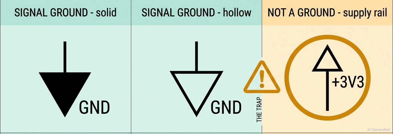
Figure: Solid and hollow signal ground symbols (GND)
Functional Earth Symbol (IEC 60417-5018)
The functional earth symbol is the earth mark drawn beneath a semicircular arc.
IEC 60417-5018 identifies a functional-earthing terminal used to support the correct operation, EMC performance, or measurement accuracy of the equipment.
The current IEC 60417 database titles it "Functional earthing". Older literature often refers to similar functional-earth concepts as "clean earth," "noiseless earth," or "low-noise ground." IEEE Std 315, Clause 3.9.1.1, includes a low-noise ground symbol and cross-references the IEC functional-earth designation.
- Measurement instruments with a separate low-noise earth stud.
- Screened rooms and EMC chambers, where the clean earth is an engineered system.
- Telecom and medical equipment often distinguish functional-earth connections from protective-earth connections.
Note: Functional earth is not protective earth. A 5018 terminal must never be used for the safety earth connection, and swapping the two is a compliance failure rather than a drafting nitpick.
Analog, Digital, and Power Ground Symbols (AGND, DGND, PGND)
AGND, DGND, and PGND are not separate standardized symbols. They are net designations commonly shown using a ground or common symbol with the corresponding name attached or included.
These designations can be used to distinguish separate ground nets that are intentionally connected at a defined point in the schematic or PCB layout.
| Net Name | Symbol Convention | What It Returns |
|---|---|---|
| GND | Plain triangle or bar | The single 0 V return on a one-ground board |
| AGND | Triangle labeled AGND | References, op-amp signal paths, converter analog side |
| DGND | Triangle labeled DGND | Logic, clocks and digital I/O |
| PGND | Triangle labeled PGND | Switching converters, motor drivers, high di/dt loops |
| GNDA, GNDD, GNDS | Manufacturer- or library-specific ground net names | Meaning depends on the component or schematic convention |
| Earth or chassis symbol | IEC 60417-5017 or 5020 | Identifies an earth or chassis/frame connection; it should not be assumed to be the same as a circuit signal ground |
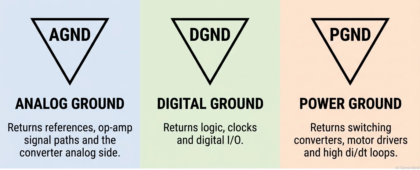
Figure: Signal ground symbols labeled AGND, DGND, and PGND.
See the difference between a pin name and a net name. Datasheets label AGND and DGND pins on converters and op-amps, but that labeling does not automatically make them separate nets. Where those nets meet on the copper is a layout question rather than a symbol question. Understanding analog and digital ground in PCB design covers that side in full.
Earth Ground vs Chassis Ground vs Signal Ground: Symbols Comparison
Earth, chassis, and signal ground use different symbol conventions because they represent different electrical roles and connection types.
One refers to earth or a structure serving that role, one identifies the equipment's frame or chassis, and one identifies a circuit common or signal reference.
| Attribute | Earth Ground | Chassis or Frame Ground | Signal or Common Ground |
|---|---|---|---|
| Symbol drawn | Three shrinking bars | Bar with three angled strokes | Solid or hollow triangle |
| Standard reference | IEC 60417-5017; IEEE 315 3.9.1 | IEC 60417-5020; IEEE 315 3.9.2 | IEEE 315 3.9.3 |
| What it physically is | Earth, or a structure serving that role | Metal chassis, frame or enclosure | Circuit common or signal reference node |
| At the Earth's potential? | Intended to be connected to earth | Not necessarily | Not necessarily |
| Carries fault current? | Yes, when it is the protective earth | Only if bonded to PE | Not intended as the protective-earth path |
| Where it lands on a PCB | Earth/protective-earth connection point, where applicable | Chassis mounting point, shield connection, or chassis-bonded hardware | Ground net, copper pour, plane, or designated return path |
| Cost of confusing it | Shock hazard or nuisance tripping | Floating metalwork, EMC failure | Noise, offset error, unstable reference |
Why These Ground Symbols Are Not Interchangeable
Draw a chassis symbol where the circuit common belongs, and you have quietly committed the board's 0 V to whatever potential the enclosure sits at.
The reverse mistake costs as much. An earth symbol on a battery-powered product claims a connection that does not exist, and the first reviewer will ask where the earth conductor goes.
Note
In a floating or isolated design, do not use an earth symbol unless an actual earth connection is intended. Use a circuit-common or signal-ground symbol when the node represents the circuit's own reference
IEC 60417 vs IEEE 315 Ground Symbols
IEC 60417 covers graphical symbols for use on equipment and products. IEEE Std 315 provides graphical symbols for electrical and electronic diagrams.
| Ground Type | IEC 60417 Number | IEEE 315 Clause | Note |
|---|---|---|---|
| Earth, general | 5017 | 3.9.1, ground general symbol | IEEE wording also covers a vehicle frame not connected to the earth |
| Functional earthing | 5018 | 3.9.1.1, low-noise ground | Cross-references the IEC "noiseless, clean earth" name |
| Protective earth | 5019 | 3.9.1.2, safety or protective ground | May replace 3.9.1 where a protective function is specified |
| Frame or chassis | 5020 | 3.9.2, chassis or frame connection | Extended to a printed-wiring board's chassis connection |
| Circuit common | Not in IEC 60417 | 3.9.3, common connections | The triangle; identification is placed inside it |
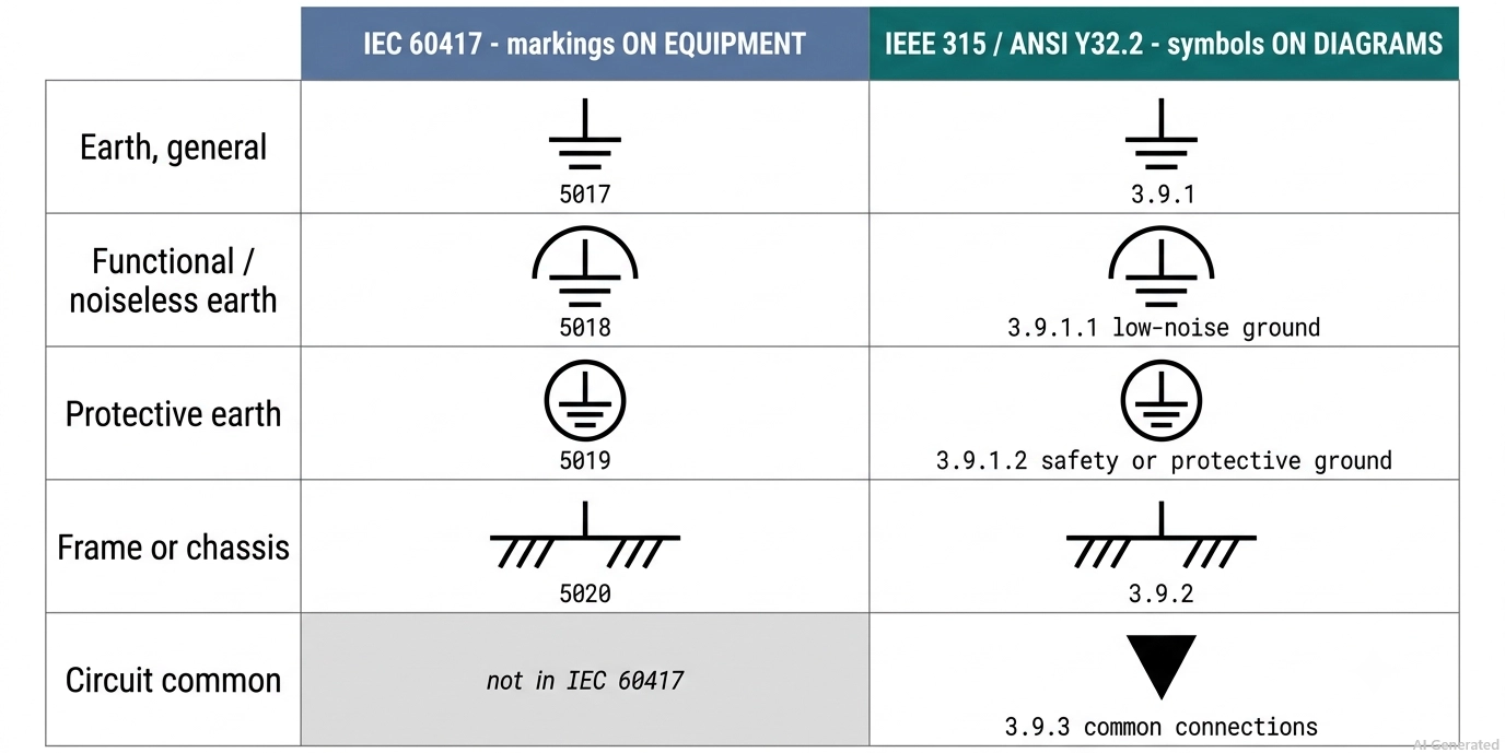
Figure: IEC 60417 and IEEE 315 ground-symbol conventions comparison
On the IEC side, diagram symbols live in IEC 60617 rather than IEC 60417. That is why a European schematic and a European equipment label can both be correct while drawing the same ground differently.
Ground Symbols in KiCad, Altium Designer, and EasyEDA
In most EDA tools, electrical connectivity is determined by the symbol's net designation and the tool's connectivity rules, not simply by the symbol's graphical appearance.
A graphical ground shape does not by itself determine the net name. If an EDA symbol is configured to connect to the GND net, changing its appearance does not necessarily create a different electrical net.
| Tool | Where the Symbols Live | Common Ground/Power Names | What Sets the Net |
|---|---|---|---|
| EasyEDA | Wiring Tools, NetFlag; Ctrl+G places GND | GND, Analog GND, Digital GND, VCC | The NetFlag name; renaming it creates a different net |
| KiCad | The `power` symbol library | GND, GNDA, GNDD, GNDPWR, GNDREF, GNDS, Earth, Earth_Clean, Earth_Protective | The power symbol's own name, which becomes a global label |
| Altium Designer | Place, then Power Port, then pick a style | Signal Ground, Power Ground, Earth, Bar, Arrow, Wave | The Net Name field, not the style |
The net name determines which net a power port connects to, not the style of the symbol. Three ports drawn as Earth, Bar and Signal Ground all join GND if all three are named GND.
How to Create a Genuinely Separate Ground Net
- Place a ground symbol and give it its own net name, such as AGND.
- Reuse that exact name everywhere the analog return belongs, on every sheet.
- Join AGND to GND at one point only, using a 0 Ω link or a net-tie component.
- Run ERC and confirm the tool reports two nets joined once, not one merged net.
Skip step three and the two nets float apart, which the tool will flag, but the bench will not.
How to Read Ground Symbols in a Circuit Diagram
Read the grounds in one pass before you trace any signal. Identify every distinct symbol, read the label on each, group like-labeled symbols into nets, then find the point where those nets meet.
- List the distinct symbols on the sheet. Three bars, a rake, a triangle and a circled earth are four different declarations.
- Read the label inside or beside each symbol. AGND and DGND are separate nets even though the shape is identical.
- Group like-labeled symbols. IEEE 315 clause 3.9.3 makes all like-designated points connected, so no wire is drawn between them.
- Find the tie point. Separate returns must join somewhere. If they never do, one of them is floating.
- Flag every circled earth. A 5019 symbol is a safety claim and needs a real protective conductor behind it.
- Trace the highest-current return last, from the load back to the source, and check it avoids sensitive nodes.
Step six is where most review findings come from. A motor return routed through the analog section shows no error in any tool, because the netlist is correct and only the physical path is wrong.
From Ground Symbol to PCB Ground Plane
A ground symbol becomes a physical PCB connection through several design steps.
The symbol establishes the intended electrical connection, the netlist carries that connectivity into PCB layout, the layout assigns copper to the net, and vias can connect that copper across layers.
| Stage | What It Is | What You Control |
|---|---|---|
| Symbol | The symbol on the schematic | Which ground type are you declaring |
| Net | The named connection, such as GND or AGND | Net name and net class |
| Copper | The plane or pour assigned to that net | Layer stack, clearance, thermal reliefs |
| Stitching via | Vias joining plane areas and layers | Via count, spacing, placement near return paths |
| Tie point | Where separate returns join | Where separate ground nets are intentionally connected |
Single-Point vs. Multi-Point Grounding
- Single-point, or star, grounding brings every return to one node. It suits low-frequency and mixed-signal boards where the return paths are predictable.
- Multi-point grounding provides multiple low-impedance connections to a common reference plane or structure. At higher frequencies and faster edge rates, continuous reference planes and closely coupled return paths are often preferred over long star-ground connections. Return current tends to follow the path of lowest impedance, which is often concentrated in the reference plane directly beneath or adjacent to the signal trace when a continuous reference plane is available.
Conclusion
A ground symbol is more than a drawing on a schematic. It identifies an electrical connection, while the net name and PCB layout determine where that connection goes. Use the correct symbol for its intended function, keep distinct ground nets clearly defined, and verify their return paths before fabrication.
FAQs About Ground Symbols
Q: What Is the Difference Between Earth Ground and Chassis Ground?
Earth ground is a connection to the planet or an equivalent structure. Chassis ground is a connection to the metalwork. IEEE 315 clause 3.9.2 warns that a chassis may sit at substantial potential with respect to earth, so the two are equal only when deliberately bonded.
Q: Is Ground the Same as the Negative Terminal?
Not always. Ground is whichever node you choose as 0 V. In a single-supply circuit, that is usually the negative terminal, but a split supply puts the negative rail below ground, and an isolated circuit may have no earth reference at all.
Q: What Is the Difference Between GND, AGND and DGND?
They are the same triangle symbol carrying different net names. GND is a single combined return, AGND carries the analog return, and DGND carries the logic return. Separating them only helps if you tie them back together at one defined point.
Q: Can One Schematic Use Different Ground Symbols?
Yes, and good schematics do. Using earth, chassis, and signal ground symbols on one sheet documents three physically different connections. What you must also show is where those nets tie together, and which single point makes that connection.
Popular Articles
• Logic Gate Symbols: The Complete Chart, Truth Tables [2026]
• The Ultimate Guide to Relay Symbol: Coil, Contacts, Diagrams, and Circuit Applications
• How to Design and Assemble a Reliable ESP32 Module PCB on a 2-Layer Board
• How to Identify SMD LED Polarity: Markings, Testing, and PCB Tips
• Power Supply Symbols Chart: A Complete Guide to AC, DC, Ground, Battery, and Source Symbols
Keep Learning
Logic Gate Symbols: The Complete Chart, Truth Tables [2026]
Note ⬇ Free Download: Logic Gate Symbols PDF Reference Chart Save time when working with digital schematics. This downloadable Logic Gate Symbols PDF includes all basic logic gates, standard symbols, truth tables, Boolean expressions, and common 74xx/4000-series IC references — a practical reference for students, engineers, and PCB designers. When we define digital logic on a schematic, we use logic gate symbols to represent Boolean operations and show how signals are processed in a circuit. A single ......
How to Read a MOSFET Symbol: NMOS, PMOS, Arrows, and Body Diodes
If you have ever opened a schematic and stared at a MOSFET symbol wondering which terminal is the source, why the gate has a gap, or why the arrow points differently on two seemingly identical symbols — you are not alone. The MOSFET schematic symbol packs four independent pieces of information into one small graphic: channel polarity, operating mode, terminal identity, and device type. Read those four cues correctly, and any MOSFET symbol becomes immediately clear, whether you encounter it in a power-......
The Ultimate Guide to Relay Symbol: Coil, Contacts, Diagrams, and Circuit Applications
Think of a standard switch as a drawbridge you lift by hand. Now, imagine a relay symbol diagram as a remote-controlled drawbridge. It allows a tiny, low-power electronic signal to control a high-power electrical load from a distance safely. Understanding how to read relay symbol configurations is the absolute cornerstone of advanced circuit design. By mastering this relay schematic symbol, you move beyond basic electronics and enter the world of professional hardware logic and safe PCB design. What Y......
How to Read Resistor Color Code: Complete Guide with Chart and Examples
4-Band Resistor Color Code Explained A 4-band resistor color code is one of the most common methods used to indicate resistance values in electronic components. It is widely used to help engineers and hobbyists quickly determine resistance values without using a resistor color code calculator. In a standard 4-band resistor: First Band (Digit 1): Represents the first significant digit Second Band (Digit 2): Represents the second significant digit Third Band (Multiplier): Indicates the factor by which t......
Solder Paste vs Flux: What's the Difference and When Should You Use Each?
Solder paste and flux are not interchangeable. Solder paste contains solder alloy powder and flux, while flux contains no solder alloy. This difference matters when choosing materials for SMT, reflow soldering, or manual soldering. Flux removes metal oxides and prevents re-oxidation, allowing molten solder to wet copper pads and component leads properly. Solder paste combines flux with fine solder alloy powder. During reflow, the flux activates to improve wetting while the solder alloy melts to form t......
Fiducial Marks in PCB and SMT Assembly: A Complete Guide to Accuracy and Design Rules
Modern Printed Circuit Boards (PCBs) are complex, integrating high-density components like 0.4mm pitch Ball Grid Arrays (BGAs), 0201 passives, and fine-pitch Quad Flat No-Lead (QFN) packages. In this advanced manufacturing environment, achieving placement accuracy measured in micrometers is crucial. A significant challenge in automated manufacturing is how pick-and-place machines, which handle thousands of components per hour, precisely locate the PCB. A board on a conveyor system is never in the perf......