Flexible PCB Price: Key Cost Factors and Ways to Save
15 min
- How Much Does a Flexible PCB Cost?
- Key Factors That Affect Flexible PCB Price
- Flexible PCB Cost Comparison for Different Designs
- How to Reduce Flexible PCB Manufacturing Cost
- Flexible PCB Manufacturing and Quotation Considerations
- JLCPCB's Flexible PCB Manufacturing Capabilities
- Conclusion
- FAQs About Flexible PCB Price
The price of a flexible PCB has no single fixed figure, as it depends mainly on the panel area occupied by the design, the number of copper layers, and the order quantity. Other features such as stiffeners, EMI shielding film, tight outline tolerance, and a complex via structure may further increase manufacturing costs. The majority of these cost factors are fixed by the PCB layout stage, and even at the time of the first quotation.
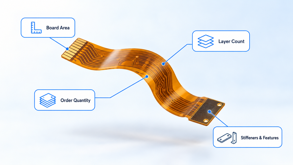
Figure: Polyimide flexible PCB with ENIG contact pads and a bonded stiffener
Here, you will learn how flexible PCB pricing is based on the quantity of orders, quantity of boards, which design specifications drive up the manufacturing costs, and why, and how flexible PCB compares to rigid PCB costs. You will also learn some useful tips and tricks for ordering and layout that will help you save money and understand what information manufacturers want to see to deliver an accurate flexible PCB quote.
How Much Does a Flexible PCB Cost?
There is no single price for a flexible PCB. JLCPCB quotes a $2.00 minimum for 5 pieces of a 2-layer board up to 100 × 100 mm. The price quoted was verified on October 23, 2026, on the flex PCB resource page. There are three rules about using it:
- Entry price, not an average: JLCPCB introduced the $2 flex price in 2024 as a special offer. It marks the floor for a small 2-layer board, not the typical cost of a production design.
- Coupons are separate: New-customer flex PCB coupons are applied at checkout and are not part of the published starting price, so confirm the current amount and validity before ordering.
- Shipping is extra: Shipping, taxes, and import duties are calculated separately from the board price.
Flexible PCB Price Examples by Layer Count and Quantity
For a price comparison of flex PCBs based on layer count and order quantity, quote a reference design and adjust only one parameter at a time. A reference build that can be used in practice:
- Outline: 50 × 50 mm rectangle, single design, no panel
- Base material: Polyimide, 25 µm dielectric
- Copper: 18 µm (0.5 oz)
- Coverlay: Yellow
- Surface finish: ENIG, 1 µin gold
- Features: No stiffener, regular vias, standard ±0.1 mm outline tolerance
Quote it at 1, 2, and 4 layers, and at 5, 50, and 100 pieces. Two trends emerge from the way the price is calculated: as the quantity increases, the price per board decreases, because the setup cost is distributed over a larger number of boards, and the higher the number of layers, the higher the price at each quantity, because more drilling, plating, or lamination is required.
Flexible PCB Prototype Cost vs. Production Cost
In a prototype order, setup makes up a large share of the price. In production, material, panel area, and processing time per panel take over.
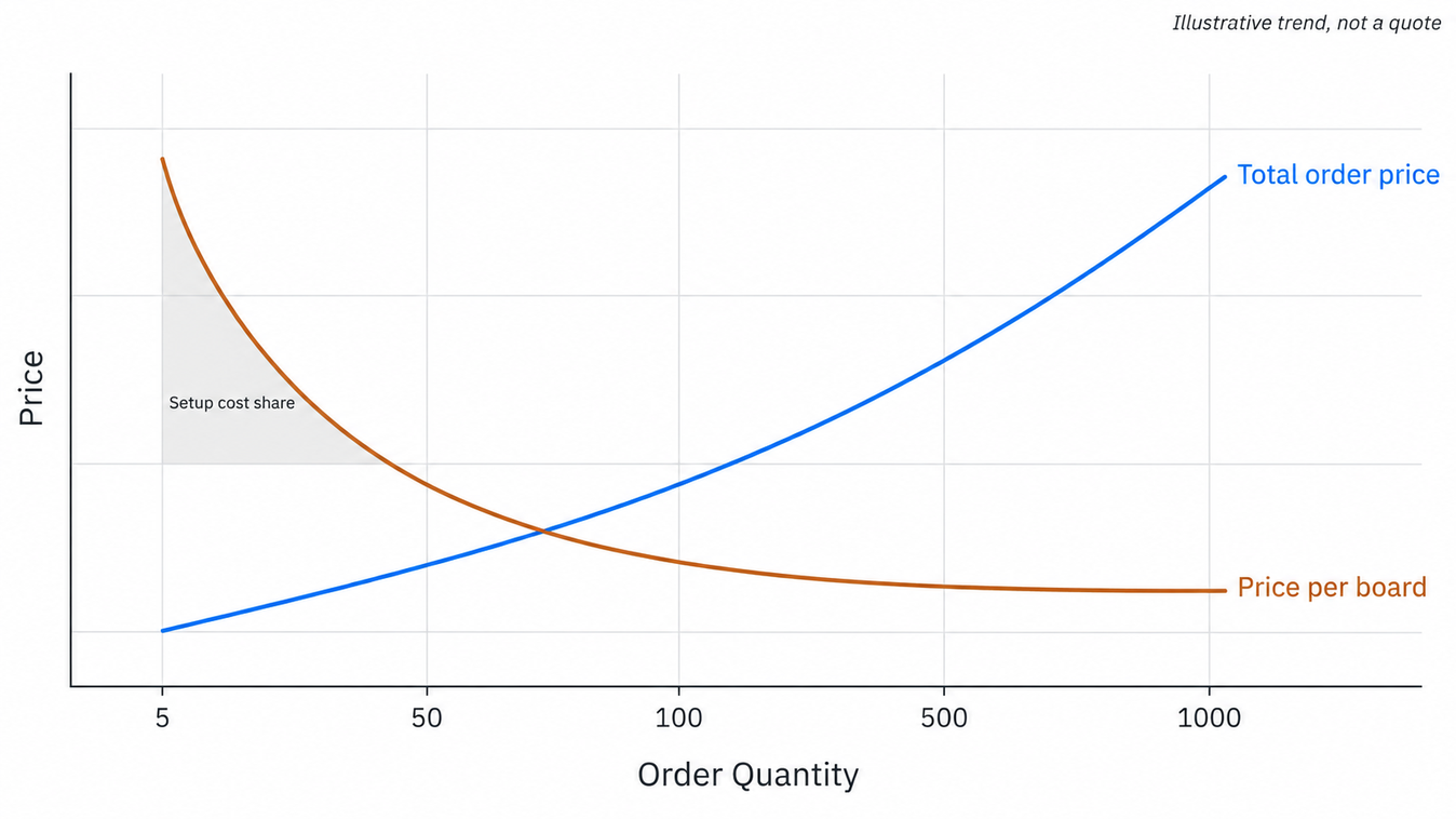
Figure: Total order price rises with quantity, while the flexible PCB price per board falls as the setup cost is shared.
- Setup cost: CAM preparation, imaging data, electrical test program, and panel layout are prepared once per design, regardless of quantity. They are ordered in the thousands, in 5-piece sets, and make up a substantial proportion of the total.
- Volume pricing: When hundreds of pieces are involved, setup costs are spread, and the area of the panel each board occupies can increase the board's cost.
- Panel efficiency: When in production, the number of boards that can fit on each panel controls the material cost per board.
- Purchasing priorities: Prototype buyers usually pay for speed and design changes. Production buyers pay for yield, consistent materials, and a predictable lead time.
Key Factors That Affect Flexible PCB Price
The cost of a flexible PCB is determined by the area of the panel a design requires, the number of copper layers, and the quantity ordered. Additional features for flex, including stiffeners, EMI shielding film, tight tolerances, and very small vias, are then added to this basic structure.
| Parameter | Effect on Manufacturing | Directional Cost Impact |
| Additional layers | More imaging, plating, lamination, and registration steps | Usually higher |
| Larger board area | More base material and panel space per board | Usually higher |
| Higher quantity | The setup cost is shared across more boards | Lower per board, generally |
| Thicker copper | Different laminates and wider minimum trace/space | Depends on the specification |
| Fine trace/space | Tighter process control during imaging and etching | Can increase cost |
| Stiffeners | Extra material and a bonding operation per stiffener type | Can increase cost |
| Tight outline tolerance (±0.05 mm) | More demanding cutting and inspection | Charged extra at JLCPCB |
| Extreme vias | Smaller drilling and plating window | Charged extra at JLCPCB |
Board Size, Layer Count, and Order Quantity
These three parameters form the basis of a flexible circuit board's cost.
- Board size: Price is based on the area of the board used by the panel, plus space and handling edges. According to JLCPCB's flex panel guidelines, the distance between boards is 2mm (3mm when using metal stiffeners), and the handling edges on all four sides are 5mm.
- Single-layer flex: Flex with no plated vias. When using a 2-layer flex, drilling and through-hole plating are added. A 4-layer flex introduces inner-layer imaging, a second lamination operation, and layer-to-layer registration.
- Order quantity: The number of boards results in a fixed cost per design to be divided; order quantity primarily influences the price per board.
Flexible PCB Materials, Copper Thickness, and Surface Finish
Material choices determine the stackup cost and the circuit's tolerance to bending and soldering.
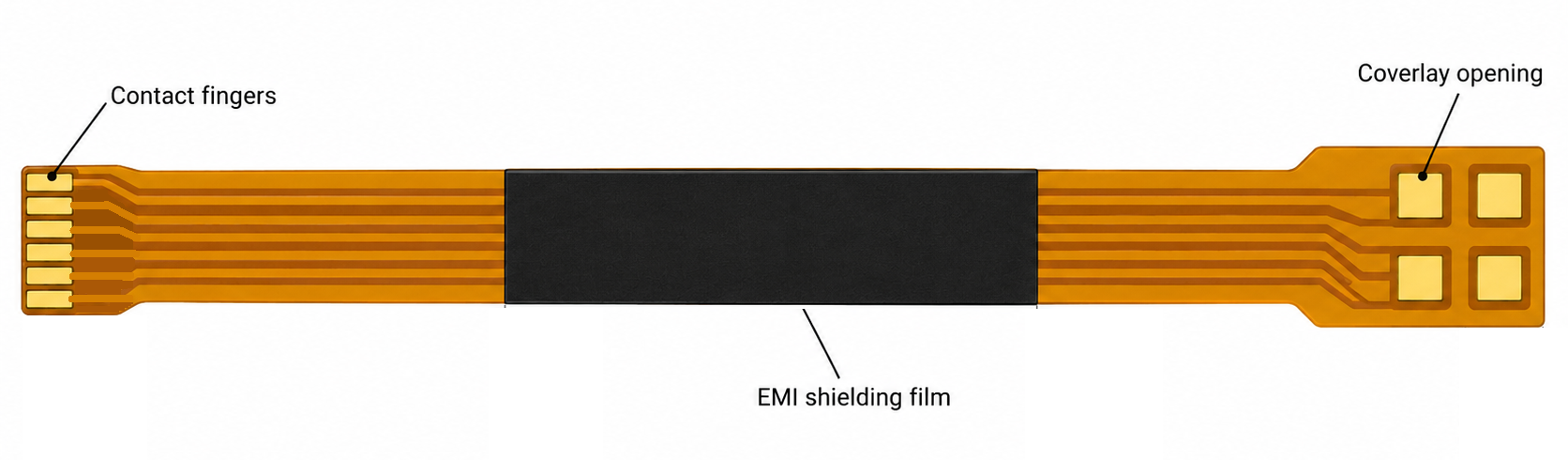
Figure: Flexible PCB with a PI stiffener at the connector, an FR4 stiffener under components, and EMI shielding film.
- Polyimide vs. PET: Polyimide is the standard flex base film because it withstands soldering temperatures. The heat resistance of PET is much less; at JLCPCB, it is known as the “transparent flex” option, so if you need transparency, choose it, but not as a low-cost alternative.
- Adhesive vs. adhesiveless laminate: Adhesiveless laminate is used for adhesion between the copper and the polyimide. It's thinner and more stable at high temperatures, and is generally more expensive than adhesive-based laminate.
- Copper type: Rolled-annealed (RA) copper is more tolerant of repeated bending than electrodeposited (ED) copper, but it is also more expensive.
- Copper thickness: The thicker the copper, the more current it can conduct, but the wider the traces and spacing must be, ranging from 3/3 mil (12µm on JLCPCB flex) to 4/4 mil (35µm on JLCPCB flex).
- Surface finish: JLCPCB flex boards come with ENIG plating, 1 or 2 µin gold. The 2 µin option doubles the gold thickness on each exposed pad, increasing material costs.
Flexible PCB Cost Comparison for Different Designs
Flexible PCB cost generally rises with construction complexity. Single-layer flex is the simplest build, double-layer flex adds plated vias, and multilayer flex adds lamination and registration; special features add cost to any construction.
Single-Layer vs. Double-Layer vs. Multilayer Flexible PCBs
The number of copper layers corresponds to more processing steps and increased stiffness, and it is a trade-off among routing density, cost, and flexibility.
- Single-layer flex: Most basic and economical flex construction. Great for sensor tails, LED strips, and dynamic bends, where everything can be routed in a single layer.
- Double-layer flex: An additional routing level and plated vias are added. It is appropriate for connector jumpers, display tails, and circuits that require a ground layer beneath the signals.
- Multilayer flex: There are four layers, which can contain dense routing and shielding layers, but the thicker stackup requires a larger bend radius. There are detailed instructions on bend design in the flexible PCB design guide.
Standard Flexible PCBs vs. Designs with Special Requirements
A standard design uses the default options: regular vias, standard outline tolerance, one coverlay color, and no stiffener. Each departure from that default adds cost:
- Custom stiffeners: Multiple stiffener materials or thicknesses on one board
- Tight tolerances: ±0.05 mm outline tolerance for a precise housing fit
- Shielding: EMI film over high-speed or noise-sensitive traces
- Bend performance: Adhesiveless laminate and RA copper for repeated flexing
Flexible PCB Cost vs. Rigid PCB Cost
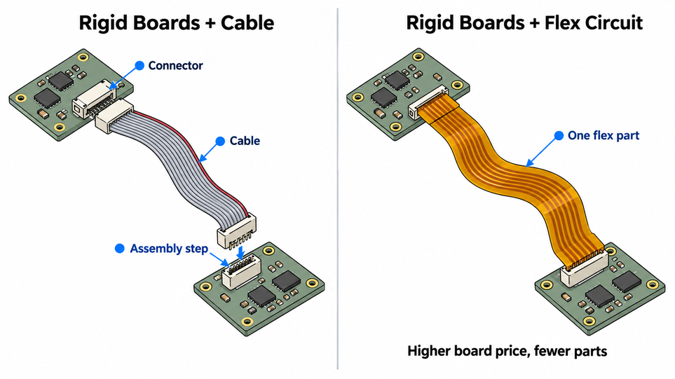
Figure: Two rigid PCBs joined by a cable and connectors compared with one flexible PCB that replaces the cable assembly.
The JLCPCB flexible PCB service page states that, due to the materials and processing, the per-piece price of a flex board is generally higher than that of a rigid board. The comparison also differs when the whole assembly is taken into account, as the rigid-PCB vs. flexible-PCB discussion illustrates.
| Construction | Additional Build Steps | Typical Use | Relative Fabrication Cost | Available at JLCPCB |
| Rigid FR-4 PCB | None (baseline): rigid laminate with solder mask | Main boards and modules | Generally, the lowest per board | Yes |
| Single-layer flex | One copper layer plus coverlay | Sensor tails, LED strips | Lowest of the flex options | Yes |
| Double-layer flex | Drilling, through-hole plating, and two coverlays | Jumpers, display tails | Higher than a single-layer | Yes |
| 4-layer flex | Inner layers, extra lamination, registration | Dense or shielded routing | Higher than a double-layer | Yes |
| Rigid-flex | Rigid and flex sections laminated into one board | Multi-board assemblies in tight spaces | Typically, the highest of the five | Not supported |
- System cost: When a flex circuit is soldered or laminated directly to both boards, it can replace a wire harness, its mating connectors, and the labor to fit them, while removing those connector contacts as failure points.
- Rigid-flex alternative: When a rigid area requires no internal routing, a flex circuit with an FR4 stiffener provides localized rigidity for components without a rigid-flex build.
How to Reduce Flexible PCB Manufacturing Cost
Minimize flexible PCB manufacturing costs in the layout, before requesting a quotation: Use the minimum number of layers that the routing permits; keep the outline as small and "nestable" as possible; specify only the materials, features, and tolerances required by the product.
Optimize Board Size, Circuit Layout, and Layer Count
- Trim unused area: Remove outline extensions that carry no circuitry, and route the outline close to the circuit.
- Reduce layers: Move from four layers to two, where the net count and shielding needs allow.
- Use manufacturable routing: Keep trace/space at or above the limit for the chosen copper, such as 3.5/3.5 mil at 18 µm.
Improve Panel Utilization and Optimize Order Quantity
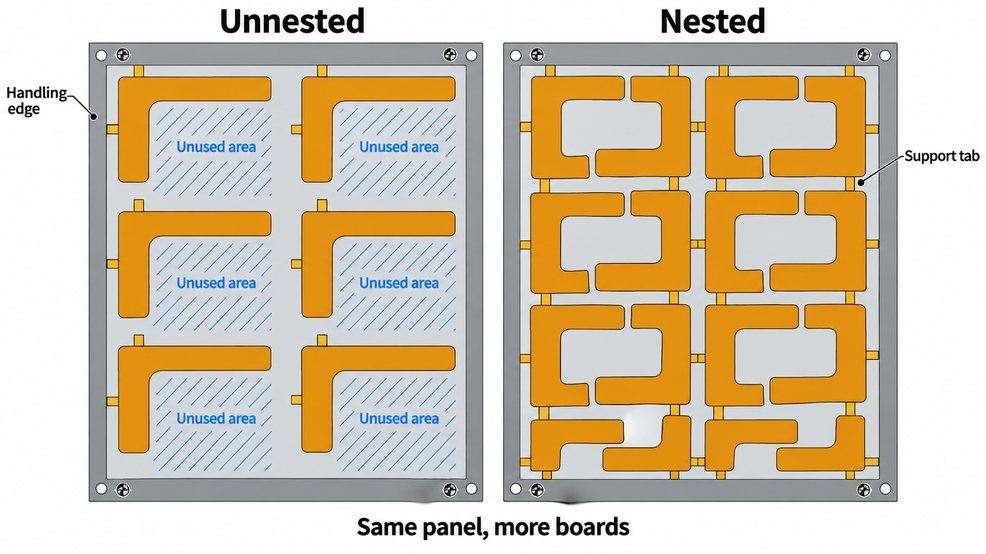
Figure: Two-panel layouts of the same flexible PCB showing how rotated, nested outlines fit more boards per panel.
- Next, the outline: L-shaped, with long, thin boards leaving unused panel area. Rotating or interlocking copies places more boards on each panel.
- Panelize small boards: JLCPCB recommends panelizing boards under 20 × 20 mm, with 0.7–1.0 mm support tabs.
- Order for the project, not the price break: A larger order lowers the price per board, but it adds cost if a design revision makes the extra boards unusable.
| Design Item | Before | After | Manufacturing Effect |
| Layer count | 4 layers | 2 layers with a ground layer | Removes inner-layer imaging and one lamination cycle |
| Vias | 0.10 mm hole, 0.3 mm diameter | 0.3 mm hole, 0.55 mm diameter | Removes the extreme-via charge |
| Outline tolerance | ±0.05 mm | ±0.1 mm | Removes the tight-tolerance charge |
| Stiffeners | FR4 and stainless steel | One stiffener type | One fewer material to bond |
| Gold thickness | 2 µin ENIG | 1 µin ENIG | Less gold deposited |
Flexible PCB Manufacturing and Quotation Considerations
An accurate flexible PCB quote requires complete fabrication data: Gerber files, outline, layer count, base material, copper thickness, coverlay, stiffener locations and quantities, and any special requirements noted in the order remarks.
What Specifications Are Needed for an Accurate Flexible PCB Quote?
- Gerber files: All copper, coverlay, silkscreen, outline, and drill layers
- Stiffener layer: A separate layer showing stiffener position and thickness, as described in JLCPCB's Gerber file preparation guide
- Dimensions and layer count: Outline size and 1, 2, or 4 layers
- Materials: Polyimide thickness, copper thickness, and coverlay color
- Finish: ENIG gold thickness
- Stiffeners and film: Type, thickness, and location of each stiffener, plus any EMI film
- Quantity: Including any panel arrangement
- Remarks: Any extra layer or requirement not covered by the standard options
How Manufacturing Processes, Testing, and Delivery Affect Cost
- Fabrication and setup: Imaging, etching, plating, coverlay lamination, and laser cutting of the outline make up the board price, and each added layer, stiffener, or film adds a step to that sequence.
- Inspection and testing: Electrical testing for opens and shorts verifies the circuit; any test or inspection report beyond the standard check is an added requirement that can increase cost.
- Assembly: Optional, and quoted separately from the bare board; PCB assembly adds component and assembly costs to the order.
- Delivery: Shipping, taxes, and import duties are charged in addition to the board price and vary by shipping method and destination.
To compare suppliers or quantities, use the landed cost of a usable board: Landed cost per board = Total order cost ÷ Usable boards received.
This is a purchasing comparison, not a manufacturer's internal cost formula. If 2 of 50 boards are damaged during assembly, the total order cost is divided by 48, not 50.
JLCPCB's Flexible PCB Manufacturing Capabilities
JLCPCB offers 1-2-4-layer flexible PCBs with polyimide thicknesses of 25 µm or 50 µm, ENIG finish, 4 coverlay colors, and 4 stiffener types. Rigid-flex boards and impedance control are not available.
Flexible PCB Options for Different Design Requirements
The values below come from JLCPCB's flex PCB capabilities page, checked October 23, 2026.
| Parameter | JLCPCB Published Capability |
| Layers | 1, 2, and 4 |
| Base material | Polyimide, 25 µm or 50 µm dielectric; transparent PET, 36 µm |
| Copper thickness | 12, 18, or 35 µm (single-sided: 18 or 35 µm) |
| Coverlay colors | Yellow, black, white, transparent |
| Surface finish | ENIG, 1 µin or 2 µin gold |
| Stiffeners | PI 0.1–0.25 mm, FR4 0.1–1.6 mm, stainless steel 0.1–0.3 mm, 3M or tesa adhesive tape |
| EMI shielding film | 18 µm, black |
| Minimum trace/space | 3/3 mil at 12 µm copper (2/2 mil absolute) |
| Maximum board size | 234 × 490 mm regular; 250 × 600 mm with edge rails, confirmed with support |
| Outline | Laser-cut, ±0.1 mm (±0.05 mm on request) |
| Impedance control | Not supported |
| Rigid-flex | Not supported |
Manufacturing Support for Flexible PCB Prototypes
The EasyEDA flex PCB design guide adds dedicated stiffener layers, and the stiffener data is exported with the Gerber files. Staying within the regular via size (0.3 mm hole, 0.55 mm diameter) and the standard ±0.1 mm outline tolerance avoids the extreme-via and tight-tolerance charges on a prototype.
How to Get a Flexible PCB Quote from JLCPCB
Step 1: Open the quote page and upload the Gerber files as one ZIP archive.
Step 2: Set the base material to Flex and confirm the layer count and dimensions.
Step 3: Select polyimide thickness, copper thickness, coverlay color, and ENIG gold thickness.
Step 4: Add stiffeners and EMI film, and name the Gerber layer that carries the stiffener data.
Step 5: Enter the quantity and any order remarks.
Step 6: Review the price, build time, and shipping, then add the order to the cart.
Conclusion
Flexible PCB price is determined primarily by panel size, the number of copper layers, order quantity, and each stiffener, EMI film, tight tolerance, and extreme via, added on top of it. Minimize the number of layers and outlines; order only what is necessary for the assembly, and order only the quantity required by the project to the extent of the routing. Such decisions reduce the cost per board used while maintaining the features that ensure reliability. Compare a few configurations in the JLCPCB online quote before placing the order.

FAQs About Flexible PCB Price
Q. What Is the Average Flexible PCB Price?
Ans: There is no meaningful average, because price depends on area, layer count, quantity, and features. JLCPCB's published starting price is $2.00 for 5 pieces of a 2-layer board up to 100 × 100 mm.
Q. Is a Flexible PCB More Expensive Than a Rigid PCB?
Ans: Generally, yes. Polyimide materials, coverlay lamination, and, where used, stiffener bonding make a flex board cost more per unit than a comparable rigid FR-4 board. A flex circuit can still lower system cost by replacing cables and connectors.
Q. How Much Does a Flex PCB Prototype Cost?
Ans: From $2.00 for 5 pieces at JLCPCB, for a 2-layer flex board up to 100 × 100 mm. Larger boards, more layers, and stiffeners raise the prototype price because setup costs are shared across only a few boards.
Q. Does the Flexible PCB Price Decrease with Order Quantity?
Ans: Yes, the price per board generally decreases as quantity increases because setup costs are shared across more boards. The total order price still rises, so order the quantity the project needs rather than the next price break.
Q. What Is the Cheapest Way to Manufacture a Flexible PCB?
Ans: Use the fewest layers the routing allows, a compact outline that nests well, regular vias, standard tolerances, and only the stiffeners the assembly needs. Single-layer polyimide flex is the lowest-cost construction in which the circuit fits on a single layer.

Keep Learning
Best Flex PCB Design Software: CAD Tools & Setup Guide
The right flex PCB design software would rely on the complexity and construction of your circuit. Altium Designer, Cadence Allegro X, OrCAD X, and Siemens Xpedition are professional tools that offer advanced capabilities for flexible and rigid-flex PCB designs, such as stackup management, bend regions, and mechanical constraints. In the meantime, for more basic flexible circuits, tools such as KiCad or EasyEDA Pro might be viable options, though they may require some manual setup and verification. Fle......
Custom FPC Fabrication: Design Rules & Manufacturing Guide
Custom FPC fabrication is the process of making flexible printed circuits in accordance with a customer's design requirements, such as board outline, layer stackup, copper thickness, openings for coverlay, and stiffener placement. Custom flexible circuits differ from traditional rigid PCBs in that they must be carefully designed and planned for materials and layout to meet flexibility and stress requirements and to fit into smaller assemblies. These design decisions are directly related to manufactura......
Polyimide Flexible PCB Fabrication: Materials and Process Guide
Polyimide flexible PCB fabrication is a process of creating thin polyimide film and copper-foil-based circuits that will bend, fold, and withstand soldering temperatures. But the same flexibility that comes from the thin film material used on these boards, and which is sensitive to moisture, makes production slightly more difficult than rigid PCBs. Polyimide can expand or contract during processing, absorb moisture before reflow soldering, and suffer from copper fatigue or cracking if the bend radius ......
Flexible PCB Price: Key Cost Factors and Ways to Save
The price of a flexible PCB has no single fixed figure, as it depends mainly on the panel area occupied by the design, the number of copper layers, and the order quantity. Other features such as stiffeners, EMI shielding film, tight outline tolerance, and a complex via structure may further increase manufacturing costs. The majority of these cost factors are fixed by the PCB layout stage, and even at the time of the first quotation. Figure: Polyimide flexible PCB with ENIG contact pads and a bonded st......
Flex PCB Design Guide: Preventing Mechanical Failures
Key Takeaways Reliable flex PCB design requires more than electrical performance. Proper bend radius control, trace routing, via placement, stiffener selection, and DFM considerations are essential to prevent mechanical failures such as copper cracking and delamination. By following proven flexible PCB design practices, engineers can improve durability and achieve reliable production results with JLCPCB. Ever wonder how the circuit in a foldable phone, fitness tracker, or camera module manages to rema......
FPC Electronics: What Is It, How It Works, Applications, and Benefits
FPC electronics is the reason your phone camera still works after a hundred open-and-close cycles. Peel apart almost any modern device, and you will find a thin amber ribbon carrying signals around corners no rigid board could turn. In this guide, you will learn: What does FPC stand for, and what are the differences between FFC and FPC? A flexible circuit that conducts a signal as it flexes The materials include one polyimide, copper, coverlay, and stiffener FPC manufacturing process (etching to elect......