Flex PCB Fabrication: Process, Materials, Design Rules & Cost
17 min
- What Is Flex PCB Fabrication?
- Materials Used in Flex PCB Fabrication
- Flexible PCB Fabrication Process: Step by Step
- Flex PCB Design Rules for Reliable Fabrication
- Flex PCB Quality Control, Testing, and IPC Standards
- JLCPCB Flex PCB Fabrication Capabilities and Ordering
- Conclusion
- FAQs About Flex PCB Fabrication
Many of the basic steps in rigid PCB fabrication also apply to flexible PCB fabrication. However, it is made with thin polyimide or PET films that can swell or shrink during processing due to moisture and temperature changes. These material attributes bring further complexities to considerations of layer alignment, coverlay openings, and bend-zone design. For instance, if there's not enough room for adhesive flow in a coverlay opening, or if a via falls in a bend zone, manufacturing defects or assembly failures may result, even if it meets the design rules.
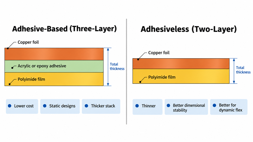
Figure: Adhesive-based and adhesiveless flexible copper-clad laminate
This guide will teach you the process and the operation of flexible PCB manufacturing, from CAM review to material preparation, laser profiling, and final inspection. You will also learn about substrate selection, copper foils, and coverlay for static and dynamic flex applications; IPC standards; quality tests; and cost factors in flexible PCB manufacturing.
What Is Flex PCB Fabrication?
The manufacturing of a printed circuit on a flexible dielectric film, typically polyimide, and then covered with a flexible protective insulating film, is called Flex PCB fabrication. The processes are similar to the ones used in rigid PCB manufacturing, but different thin-film handling, alignment, and profiling are required.
How Flexible PCBs Are Constructed
A flexible circuit is a construction consisting of copper conductors, a flexible dielectric film, adhesive, and a coverlay. The number of copper layers indicates the construction:
- Single-sided flex: The base material is polyimide, covered with a single copper layer, and the coverlay is the thinnest and most flexible.
- Double-sided flex: Copper on both sides of the base film, and joined by plated through-holes.
- Multilayer flex: Three or more layers of copper with adhesive films between them, used for routing that is not possible with two layers.
A stiffener will not make a flex circuit a rigid-flex board. The stiffener is a bonded support plate and has no electrical connection to the circuit. A rigid-flex board laminates the flexible sections into rigid multilayer sections and links them with plated TH.
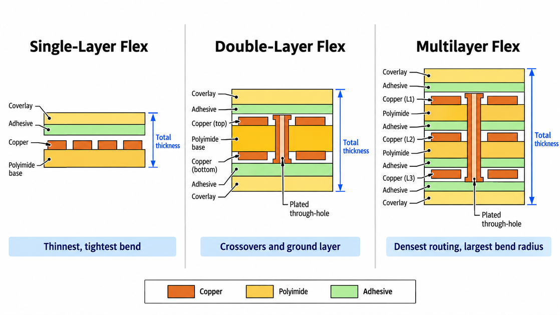
Figure: Flex PCB fabrication layer stackups for single-sided, double-sided, and multilayer flexible circuits.
Rigid PCB vs. Flexible PCB Fabrication
The same imaging, etching, and plating chemistry is used for both rigid and flexible PCB fabrication. They differ about materials, handling, protection, and profiling:
| Process Area | Rigid PCB Fabrication | Flexible PCB Fabrication |
| Substrate | Glass-reinforced FR-4 laminate | Polyimide or PET film |
| Protective layer | Liquid photoimageable solder mask | Polyimide coverlay or flexible solder mask |
| Drilling | Mechanical drilling of stacked panels | Mechanical or laser drilling, with support material |
| Handling | Self-supporting panels | Film needs carriers, frames, or careful handling |
| Profiling | CNC routing or V-scoring | Laser cutting or die cutting |
| Assembly support | The board is rigid on its own | Stiffeners and carrier fixtures support SMT |
Thin film is not as dimensionally stable as glass-reinforced laminate. Polyimide will expand and shrink with heat and moisture, and every artwork is scaled and aligned to measured targets by fabricators.
Static vs. Dynamic Flex Applications
A static flex circuit is being flexed during installation and is then left with a permanent bend. A dynamic flex circuit flexes many times during use, such as in a printer head cable or a hinge.
- Static flex: Can be bent tighter, tolerates ED copper, and has two or more layers of copper in the bend.
- Dynamic flex: Preferable RA copper, 1 copper layer in bend area, adhesiveless laminate, larger bend radius – tested.
Materials Used in Flex PCB Fabrication
Flex circuit materials can be broken down into four categories: dielectric film, laminate construction, copper foil, and protective and support layers. Both affect bending life, solderability, and cost.
| Material | Primary Function | Selection Factor |
| Polyimide | Flexible dielectric | Thermal stability and bending requirements |
| PET | Alternative dielectric | Cost and process-temperature limits |
| RA copper | Conductor | Repeated bending applications |
| ED copper | Conductor | Cost and application-dependent fatigue requirements |
| Coverlay | Insulation and protection | Flexibility and pad-opening alignment |
| Stiffener | Local mechanical support | Connector thickness and assembly support |
Polyimide and PET Flexible Substrates
The flex dielectric of choice is polyimide, which maintains mechanical and electrical characteristics at soldering temperatures. PET is more affordable and supplied in a clear film, but has a much lower temperature resistance. Generally, it can be used only for designs that do not use a standard lead-free reflow process. The flex PCB stackup design guide covers the total thickness of the flex PCB, depending on the type of dielectric used.
Adhesive-Based vs. Adhesiveless Copper-Clad Laminates
There are 2 constructions of flexible copper-clad laminate:
- Adhesive-Based (Three-Layer): Copper bonded to polyimide with adhesive (either acrylic or epoxy). It is less expensive and is appropriate for most static designs.
- Adhesiveless (Two-Layer): Copper directly bonded to polyimide. Thinner, more dimensionally stable, and more resistant to repeated bending.
Acrylic adhesive tends to swell significantly in thickness when heated. In plated holes that pass through adhesive layers, this expansion can stress the copper barrel during reflow.
Rolled-Annealed vs. Electrodeposited Copper for Flex Circuits
The bending fatigue of copper foil type has a direct impact:
- Rolled-annealed (RA) copper: The rolled grain structure slows crack expansion when subjected to repeated bending, resulting in the typical use of RA copper for dynamic flex. This will be a bit more expensive than ED foil.
- Electrodeposited (ED) copper: Cracks after fewer bending cycles, but it is cheaper and good for static and installation bends. There are qualified grades for flexing some EDs.
Thinner copper will create less strain in a bend; thus, use the thinnest copper that can handle the current in the flex zone.
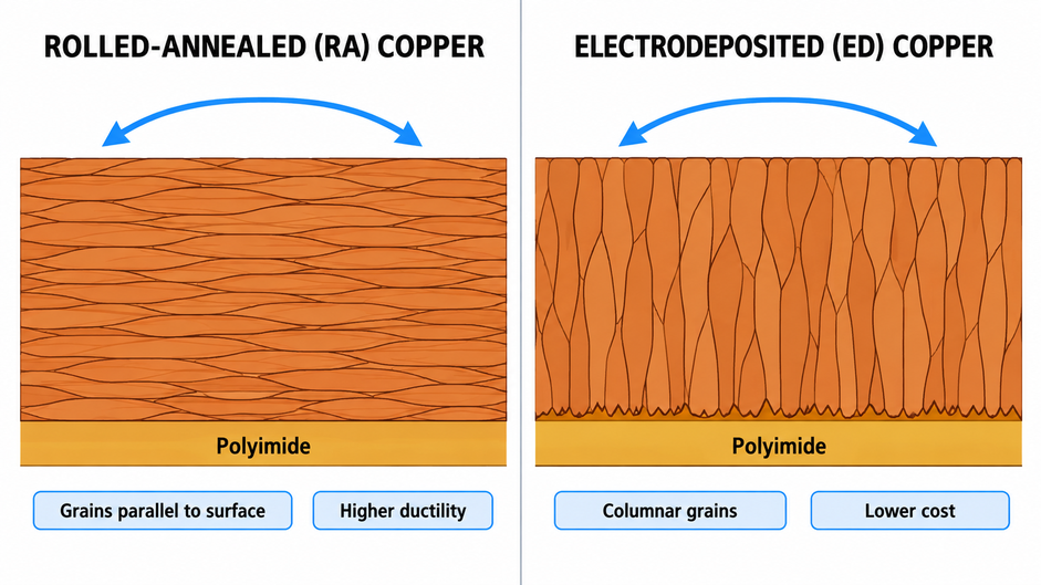
Figure: Rolled-annealed and electrodeposited copper grain structures in flex PCB fabrication.
Flexible PCB Fabrication Process: Step by Step
The flexible PCB manufacturing process includes CAM, imaging, drilling, plating, lamination, coverlay, finishing, profiling, and testing. The order is based on the number of layers, via structure, and whether the fabricator uses panel or pattern plating.
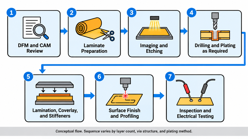
Figure: Flexible PCB fabrication process flow from DFM and CAM review to electrical testing and final inspection.
The flow is conceptual in nature. Typically, drilling and hole metallization occur before outer-layer imaging on a double-sided board. A 4-layer board is etched and imaged in the interior layers first, followed by lamination, drilling, and then plating.
Step 1: Design Review, CAM Preparation, and Material Cutting
CAM engineers verify Gerber and drill files to the fabricator's design rules before cutting film.
- Check the data: Compare copper, drill, coverlay, outline, and stiffener layers with the stated stackup.
- Plan the panel: Add handling edges, fiducials, tooling holes, and support tabs.
- Compensate for dimensional change: Scale the artwork so the circuit finishes at the correct size after the film shrinks or expands during processing.
- Cut the laminate: Cut sheets from copper-clad film rolls, and bake them where moisture removal is required.
Step 2: Circuit Imaging, Developing, and Copper Etching
The circuit pattern is transferred to the copper with a dry-film photoresist, which is then etched to remove unprotected copper.
- Laminate the resist: Apply dry-film photoresist to the cleaned copper.
- Expose the pattern: Use laser direct imaging (LDI) or a phototool. LDI writes from CAM data and can rescale each panel to its measured fiducials.
- Develop: Remove the unexposed resist.
- Etch and strip: Etch the exposed copper, then strip the remaining resist.
Undercut occurs when the etchant dissolves away the copper sidewalls of the trace, and is a problem with thin traces. Because of this, the minimum trace and space increase as copper thickness goes up; fabricators add width to the artwork to compensate.
Step 3: Drilling, Desmear, and Hole Metallization
Holes should be made and plated only where necessary to join layers. A single-sided circuit without plated holes skips metallization.
- Mechanical drilling: Drills through-holes, usually with entry and backup material supporting the film.
- Laser drilling: Ablates microvias and very small holes. Mechanical and laser drilling are alternatives chosen by hole type and size.
- Desmear and cleaning: Removes drilling residue. Many flex fabricators use plasma where the construction requires it, because the alkaline permanganate desmear used for rigid boards is less suitable for polyimide and acrylic adhesive.
- Metallization: Electroless copper or direct metallization makes the hole wall conductive, then electrolytic copper builds the barrel.
Later steps will be done in the order defined by the plating method. Panel plating, pattern plating, and button plating are the types of plating that can be used. Panel plating plates the whole panel before etching, pattern plating plates only the imaged traces and holes, and button plating plates only the pads and holes to keep the copper in the bend-zone thin.
Step 4: Multilayer Lamination and Optical Inspection
Multilayer flex bonds etch the inner layers into a single stack, and automated optical inspection (AOI) checks each layer before lamination hides it.
- Layer alignment: Inner layers are registered with tooling holes or optical targets.
- Bonding: Adhesive films bond the layers under controlled heat, pressure, and vacuum.
- AOI: Cameras compare etched copper with the CAM data to find opens, shorts, nicks, and width deviations.
Step 5: Coverlay Application, Stiffener Bonding, and Surface Finishing
The circuit is covered with coverlay, and exposed pads are covered with surface finish, and stiffeners are provided for local support.
- Form coverlay openings: Cut pad openings with a laser, drill, or punch before lamination.
- Align and press: Align the openings to the pads, then laminate the coverlay in a hot press, often under vacuum. The adhesive flows slightly into each opening.
- Finish the pads: Apply the surface finish to exposed copper. ENIG is common for flex. OSP, immersion silver, immersion tin, and hard gold are industry options that a fabetcher supports.
- Boa single stiffeners: Attach stiffeners with a thermosetting adhesive in a hot press or with a pressure-sensitive adhesive.
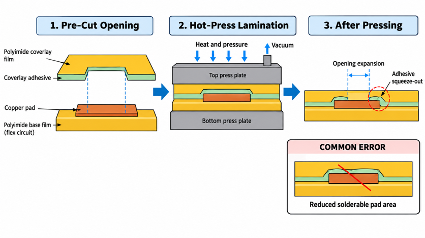
Figure: Coverlay lamination in flex PCB fabrication showing adhesive squeeze-out into a pad opening.
Step 6: Laser Profiling, Electrical Testing, and Final Inspection
The last step is to separate the circuits and check the connections and dimensions.
- Laser profiling: No cutting die; laser cuts out the outline according to CAM data.
- Die cutting – Outline is punched with a steel-rule or hard-tool die. More expensive to set up, but faster in volume.
- Electrical tests: The puncher verifies netlist continuity and isolation with a flying-drill fixture.
- Final inspection and packaging: Inspection of dimensions, coverlay, and stiffeners. Polyimide retains moisture, and circuits are typically vacuum-packed to prevent moisture absorption.
Flex PCB Design Rules for Reliable Fabrication
Design rules for flex PCBs are the link between the layout and the buildable circuit during the process, and the survivable circuit in use. These include trace and via geometry, bending, coverlay openings, and stiffeners.
The majority of flex fabrication issues can be attributed to five layout decisions:
| Design Mistake | Manufacturing Consequence | Prevention |
| Via in a dynamic bend zone | Barrel or pad cracking after flex cycles | Keep holes 1.5 mm or more from a dynamic bend zone |
| Stiffener edge on the bend line | Strain concentrates and traces a fracture at the edge | Offset stiffener edges from the bend |
| Coverlay opening equal to the pad | Adhesive squeeze-out reduces the solderable pad area | Apply the fabricator's opening expansion |
| Traces are stacked on both layers in the bend | Higher stiffness and early conductor cracking | Stagger traces between layers |
| Solid copper pour in the bend area | Stiff bend and cracking under repeated flexing | Use hatched copper |
Minimum Trace Width, Spacing, and Via Design
Minimum trace and space depend on copper thickness, because thicker copper etches longer and undercuts more. JLCPCB's published flex limits show the effect:
- 12 µm copper: 3/3 mil regular. 2/2 mil is an absolute limit to avoid where possible.
- 18 µm copper: 3.5/3.5 mil.
- 35 µm copper: 4/4 mil.
A shift from 12 µm to 35 µm copper will increase trace width and spacing by approximately 1 mil. JLCPCB's regular via has a hole size of 0.3mm, a pad size of 0.55mm, and a PTH hole annular ring of not less than 0.25mm
Bend Radius and Neutral Axis Design
Bend radius is measured on the inside surface of the bend. The safe value depends on the total thickness, the number of copper layers in the bend, the type of copper, the laminate construction, and the number of flex cycles. There is no one correct multiplier for all designs. According to JLCPCB's own guidance, the spread is:
- Capability page: Static bends at 6× total thickness for single-layer and 10× for multilayer, and dynamic bends at 10–15× or more.
- Flexible PCB bend radius guide: 6× and 12× for static bends, and 100× to 150× for dynamic bends.
The neutral axis causes the spread. A plane within a bent stack is not strained, and the strain of a conductor is about the distance from that plane divided by the bend radius. The strain is approximately 1% at a copper thickness of 0.05 mm from the neutral axis, at a radius of 5 mm.
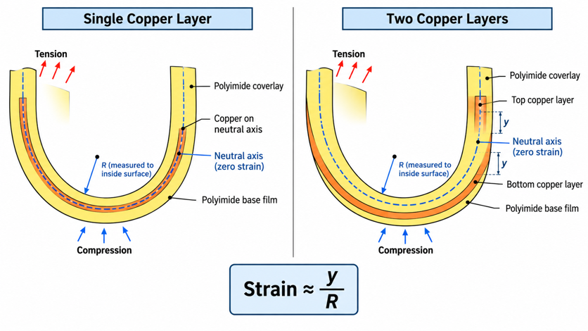
Figure: Flex PCB bend radius and neutral axis position in single-layer and double-layer flexible circuits.
Flex PCB Quality Control, Testing, and IPC Standards
Flex PCB quality control combines design standards, acceptance specifications, in-process inspection, and reliability testing.
IPC-6013, IPC-2223, and Inspection Requirements
Two IPC documents cover flexible boards:
- IPC-2223: The sectional design standard for flexible and rigid-flex printed boards, used with the generic IPC-2221 design standard.
- IPC-6013: The qualification and performance specification for flexible and rigid-flex printed boards, covering inspection and test of the finished board.
IPC-6013 defines the performance classes. Class 2 refers to dedicated-service electronic products, and Class 3 refers to high-performance products where continuous operation is essential. The class is specified in the procurement documents, and a flex circuit is not automatically built to Class 3. Verify the class being fabricated and inspected.
Common Flex PCB Fabrication Defects
Most flex defects have a known cause that design or process control can prevent:
| Defect | Typical Cause | Prevention |
| Delamination | Absorbed moisture or contamination | Baking, clean surfaces, controlled storage |
| Registration error | Dimensional change of the film between process steps | Scaling compensation and optical alignment |
| Adhesive squeeze-out | Coverlay openings without a flow allowance | Correct opening expansion |
| Trace undercut | Over-etching on thicker copper | Etch compensation and suitable trace width |
| Conductor fracture | Tight bend radius or ED copper in dynamic flex | Larger radius and RA copper |
| Plated-hole defects | Poor desmear or plating | Suitable hole cleaning and plating control |
Electrical and Mechanical Reliability Testing
Some tests confirm the circuit was built correctly. Others confirm it will survive its service life:
- AOI: Detects etching defects on each layer during fabrication.
- Electrical test: Confirms continuity and isolation on finished circuits.
- Microsection: Cross-sections a sample to check plating thickness, bonding, and hole quality.
- Peel strength: Measures the adhesion of copper and coverlay to the base film.
- Dynamic flex fatigue testing: Bends samples repeatedly at the design radius, where the application specifies a cycle count.
The first four validate manufacturing quality. Flex fatigue testing validates the bend design and is usually a qualification test on prototypes.
Flex PCB Prototyping vs. Volume Production
One-time setup typically is the most expensive aspect of a flex PCB prototyping order. Typically, material area is the primary factor in volume production. Laser profiling is useful for prototypes and design iterations, as no special cutting die is required. It does not cover all setup charges, since the CAM work, imaging data, test programs, and panel layout must be prepared for each design. A cutting die is cost-effective per circuit with high volumes.
JLCPCB Flex PCB Fabrication Capabilities and Ordering
JLCPCB is a 1, 2, and 4-layer flexible circuit board manufacturer with polyimide or PET film, ENIG finish, LDI imaging, and laser-cut outlines.
JLCPCB Flex PCB Manufacturing Capabilities
Values based on the JLCPCB flex PCB capabilities page. Exceptional limits may involve extra charges or require verification:
| Specification | Regular Capability | Limit or Note |
| Layer count | 1, 2, and 4 layers | Rigid-flex is not yet supported |
| Base dielectric | Polyimide, 25 µm or 50 µm | Transparent PET, 36 µm |
| Copper thickness | 12, 18, or 35 µm (2- and 4-layer) | Single-sided: 18 or 35 µm |
| Minimum trace/space | 3/3 mil on 12 µm copper | 2/2 mil absolute limit |
| Via hole/pad | 0.3 mm / 0.55 mm | 0.10/0.3 mm (2-layer) or 0.15/0.35 mm (4-layer) at extra cost |
| PTH annular ring | 0.25 mm or more recommended | 0.18 mm absolute limit |
| Surface finish | ENIG, 1 or 2 µin gold | Only finish the listed |
| Stiffeners | PI, FR4, stainless steel, 3M adhesive tape | EMI shielding film available |
| Maximum size | 234 × 490 mm | 250 × 600 mm with edge rails, confirm with support |
| Outline tolerance | Laser cut, ±0.1 mm | ±0.05 mm on request |
| Impedance | Not supported | Trace width control only |
All the prefixes are listed in the FPC stiffener and layer-naming guide. Placing a stiffener will switch to the board type of FPC and open the 2 stiffener layers in EasyEDA Pro. Before submission, check that no vias are located in the bend zone and that the outline of each stiffener is consistent with its order field.
Conclusion
The first step in a successful flex PCB fabrication is choosing the appropriate materials for the job, factoring in the desired flex properties, and planning for the manufacturer's production capabilities. Selecting the correct substrate, copper foil, opening coverlay areas, bend zones, and stiffening areas are all design choices that will impact the board's manufacturability, cost, and long-term reliability.
Before submitting your design for manufacturing, check the stackup and critical dimensions, and ensure your manufacturing files are appropriate for the manufacturer. Early attention to these details can help minimize manufacturing defects, eliminate unnecessary costs, and enhance the performance of the completed flexible circuit. When your design is complete, you can upload your Gerber files to get a flex PCB quote and then go on to prototype your design.
FAQs About Flex PCB Fabrication
Q. How Long Does Flexible PCB Fabrication Take?
Ans: Build time depends on layer count, stiffeners, and special processes. JLCPCB's flexible PCB page lists 4–5 day lead times for standard flex orders. The quote shows the build time for the selected options, and shipping is separate.
Q. What Is the Difference Between Flex PCB Fabrication and Rigid PCB Fabrication?
Ans: Flex PCB fabrication uses polyimide or PET film instead of FR-4, protects traces with coverlay instead of liquid solder mask, compensates for film movement, and cuts outlines by laser or die instead of routing.
Q. Why Is Plasma Treatment Used in Flexible PCB Manufacturing?
Ans: Plasma removes drilling residue and activates hole walls before metallization, where the construction requires it. Alkaline permanganate desmear is less suitable for polyimide and acrylic adhesive. Circuits without plated holes may not need it.
Q. Can Flexible PCBs Be Assembled Using Standard SMT Equipment?
Ans: Yes, with support. Flex circuits are usually fixed to a rigid carrier for printing, placement, and reflow, and pre-baked to remove moisture.
Q. Does Flex PCB Prototyping Require Dedicated Tooling?
Ans: Not for the outline. A laser-profiled prototype needs no dedicated cutting die. However, each design still needs CAM preparation, imaging data, a test program, and a panel layout, so a one-time setup cost remains.
Keep Learning
Flex PCB Fabrication: Process, Materials, Design Rules & Cost
Many of the basic steps in rigid PCB fabrication also apply to flexible PCB fabrication. However, it is made with thin polyimide or PET films that can swell or shrink during processing due to moisture and temperature changes. These material attributes bring further complexities to considerations of layer alignment, coverlay openings, and bend-zone design. For instance, if there's not enough room for adhesive flow in a coverlay opening, or if a via falls in a bend zone, manufacturing defects or assembl......
Smart PCB Array Design for Higher Yield and Lower Production Costs
Key Takeaways Smart PCB array design is a critical strategy for achieving higher manufacturing yield and significantly lower production costs. By optimizing panelization with proper board spacing, V-scoring, tab routing, and mouse bites, designers can dramatically improve material utilization by 20-30%, enhance production throughput, and simplify handling and depaneling while minimizing mechanical stress and defects. Effective use of fiducials and careful component clearance further ensures high-quali......
Why Accurate NPTH Design Matters for Reliable PCB Manufacturing
Key Takeaways NPTH are mechanical holes (no copper plating) used for mounting, alignment, and tooling. Poor NPTH design often causes PCB cracks during assembly or screw tightening. Follow key rules: ±0.08 mm tolerance, ≥0.5 mm diameter, 0.2–0.3 mm copper clearance. Keep adequate material around edge holes and clearly mark NPTH in fabrication files. Proper NPTH design + DFM checks ensure reliability from prototype to mass production. Ever get a slight crack in a finished PCB when putting it into an enc......
Gerber of PCB: A Comprehensive Guide
Introduction: Printed Circuit Boards (PCBs) are the backbone of modern electronics, serving as the platform on which components are mounted and interconnected. One of the most critical elements in PCB design and manufacturing is the Gerber file. Gerber files are the standard format used to communicate the design of a PCB to the manufacturer. These files provide precise information about the PCB layers, component placement, copper traces, and more. Understanding Gerber files is essential for anyone inv......
Electronic Board Manufacturing: Efficient Strategy and Quality Control Processes
Electronic board manufacturing is a critical process in the electronics industry, and the quality of the boards produced can significantly impact the performance and reliability of the final product. Therefore, it is essential to follow efficient strategies and quality control processes throughout the manufacturing process to ensure the highest quality of the boards. In this article, we will explore the various steps involved in electronic board manufacturing, including materials selection, design and......
Best Practices for Successful Electronic Manufacturing
Key Takeaways Mastering best practices in electronic manufacturing — from optimized PCB design and DFM to rigorous testing, verification, and high-quality production — is essential for achieving reliable, cost-effective, and timely electronic products. By following proven methodologies, leveraging advanced tools like EasyEDA, and partnering with a trusted manufacturer such as JLCPCB, designers and engineers can significantly reduce errors, accelerate time-to-market, and ensure superior performance acr......