DIY PCB Stencil: How to Make a Solder Paste Stencil
18 min
- Quick Answer: Can You Make a DIY PCB Stencil?
- What You Need: DIY Stencil Materials
- How to Make a DIY PCB Stencil, Step by Step
- How DIY PCB Stencils Are Made: Cutting Methods Compared
- DIY Stencil Comparison: Cost, Accuracy, Pitch, and Reuse
- Common DIY PCB Stencil Mistakes
- The Limits of DIY Stencils: Where They Break Down
- When Does It Make Sense to Order a Steel Stencil?
- FAQ about DIY PCB Stencils
- Conclusion: Making Your DIY PCB Stencil
Key Takeaways
DIY is possible: You can make a working solder paste stencil from Kapton, Mylar, or vinyl using a craft knife, vinyl cutter, or laser for larger SMD components and low-volume prototyping.
0.5 mm pitch is the practical boundary: DIY stencils work well above 0.5 mm pitch but struggle with finer QFNs, QFPs, and BGAs due to poor aperture quality and paste release.
Match thickness to your smallest pad: Use 0.10–0.15 mm (4–6 mil) sheet stock, choosing thinner material for smaller pads and thicker for larger pads that need more paste volume.
Test before cutting: Always run scale tests and material tests on scrap before cutting your final stencil to avoid wasting material and time.
Know when to order steel: For fine-pitch parts, repeated builds, exposed thermal pads, or production records, a professional laser-cut steel stencil is usually cheaper and more reliable than DIY tuning.
You have the SMD board, a tube of solder paste, and you're starting to realize that dabbing paste pad-by-pad is messy, slow, and inconsistent. Of course, you begin to question if you can make your own DIY PCB stencil. This guide describes how to make a working DIY PCB stencil, including the materials, cutting methods, and a step-by-step process for preparing and applying solder paste. It also draws a clear line between when DIY makes sense and when it doesn't. DIY works well for larger packages and quick prototypes, while fine-pitch components, repeated builds, and more demanding boards often justify a professionally cut steel stencil.
Quick Answer: Can You Make a DIY PCB Stencil?
Yes, you can make a DIY PCB Stencil. You can cut a working solder paste stencil from Kapton, Mylar, vellum, or blade-safe vinyl using a craft knife, vinyl cutter, or laser. While it works well for larger SMD components and low-volume prototyping, it struggles below 0.5 mm pitch due to poor aperture quality and paste release.
- Kapton, Mylar, and vinyl are the most practical DIY stencil materials. Use approximately 0.10–0.15 mm (4–6 mil) sheet stock, choosing thinner material for smaller pads. Hand cutting suits simple and large apertures, while craft cutters and CO₂ lasers provide better repeatability.
- Treat approximately 0.5 mm pitch as the practical DIY boundary, not a guaranteed capability.
- Film stencils usually survive a handful to a few dozen prints, depending on the material and cleaning method.
- Quad Flat No-Lead (QFN) thermal pads, 0.4 mm leads, and BGAs expose DIY's weakest point: paste release.
- A steel stencil may cost less than the time spent tuning a difficult homemade PCB stencil.
What You Need: DIY Stencil Materials
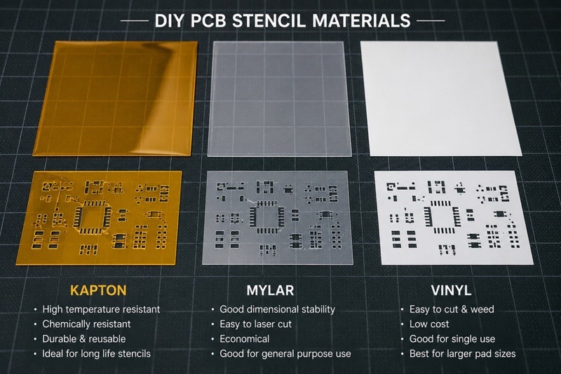
The best PCB stencil material is not simply the toughest sheet. It is the thinnest material your tool can cut cleanly without stretching, melting, or leaving ragged aperture walls. For more background on foil types and framed versus frameless construction, see this guide to SMT stencils.
For most DIY PCB stencils, choose sheet stock between 0.10 mm and 0.15 mm (4–6 mil). Thinner foil suits fine-pitch pads because it deposits less paste; thicker foil works better for larger pads where you need more paste volume. Match the thickness to your smallest pad, not your largest one.
| Material | Typical Thickness | Best Tool | Best For | Expected Reuse | Watch-Outs |
|---|---|---|---|---|---|
| Kapton/polyimide | 0.08–0.13 mm (3–5 mil) | CO₂ laser or sharp blade | Heat resistance and repeated prototypes | About 20–30 prints | Costs more, diode lasers may char the edges |
| Mylar/PET/transparency film | 0.10–0.15 mm (4–6 mil) | Craft cutter or CO₂ laser | Low-cost prototypes and larger passives | About 5–10 prints | Can melt, curl, or cloud with the wrong solvent |
| Blade-safe vinyl | 0.08–0.15 mm (3–6 mil) | Vinyl or craft cutter | Fast one-offs with generous pads | A few boards | Flexible and easy to distort; do not laser-cut PVC |
| Vellum paper | 0.09–0.13 mm (3.5–5 mil) | Knife or craft cutter | Very cheap tests and simple boards | Up to about 10 prints | Tears and loses edge definition sooner, but can be cleaned with IPA for limited reuse. |
| Thin stainless steel | 0.08–0.15 mm (3–6 mil) | Suitable fiber laser | Repeat builds and fine features | Production-reusable | Requires specialist equipment and safe metal processing |
How to Make a DIY PCB Stencil, Step by Step
1.Inspect the PCB and choose the side.
Identify the smallest component pitch, smallest pad, and any exposed thermal pads. Make one stencil for the top paste layer and a separate stencil for the bottom if both sides contain SMD components.
2.Export the solder paste layer.
Generate only the layer that maps the paste apertures, then inspect it in a Gerber viewer. Retain the board outline or add two registration marks outside the active paste area.
Exporting the Solder Paste Layer
In KiCad, select F.Paste or B.Paste when generating fabrication outputs. KiCad's official documentation identifies the *.Paste layers as the layers used for solder paste stencil manufacturing. With Protel-style extensions enabled, the usual files are GTP for top paste and GBP for bottom paste. For more details, see our guide to the solder paste layer and the KiCad Gerber-generation help documentation for exporting paste layers correctly.
Altium calls the layers Top Paste and Bottom Paste. EasyEDA uses TopPasteMaskLayer and BottomPasteMaskLayer, while Autodesk EAGLE and Fusion Electronics use the tCream and bCream layers. The naming varies, but Top Paste, Bottom Paste, Cream Layer, and Paste Layer all refer to the same thing: the map of stencil openings where solder paste will be deposited. Then convert the Gerber file into a cutter-compatible format such as SVG or DXF before preparing the physical stencil material in the cutting machine. The complete standard is available through IPC's IPC's IPC-7525C stencil-design documentation.
3.Tune difficult apertures.
For closely spaced pads, begin by reducing the aperture area by approximately 10–20%. Use a window-pane pattern instead of one large opening on an exposed QFN or DFN thermal pad.
4.Convert the design into cutter paths.
Plot an SVG directly when your EDA software supports it or open the GTP or GBP Gerber in Gerbv and export an SVG. Gerbv is an open-source Gerber viewer with SVG and DXF export functions.
5.Clean the vector file.
Open the SVG in your cutter software or a vector editor. Confirm that the aperture paths are closed, remove duplicate outlines, and preserve a 1:1 scale.
6.Run a scale test.
Cut or draw a 10 mm square and measure it with callipers. Correct any scaling error before cutting the actual PCB stencil.
7. Run a material test.
Test several combinations of blade force, speed, laser power, and passes on scrap material. LightBurn's Material Test tool can help generate a test pattern for laser users.
8. Secure the physical material.
Put the film on a clean, low-tack cutting mat or a flat laser bed. Tape outside the active area so the stock cannot lift, buckle, or move.
9.Cut the real apertures.
Import the prepared path into the cutting machine and start the job. The blade or laser now follows the on-screen vectors and physically removes material at every solder paste opening.
10.Weed, clean, and inspect the stencil.
Remove loose islands with fine tweezers. Clean compatible film with isopropyl alcohol and inspect it against a backlight. Reject merged, tapered, partially cut, or visibly distorted openings.
11.Build a registration jig.
Place spare PCBs or equal-thickness offcuts around the target board so it cannot move. Tape one edge of the stencil to create a hinge and practice lifting it straight upward.
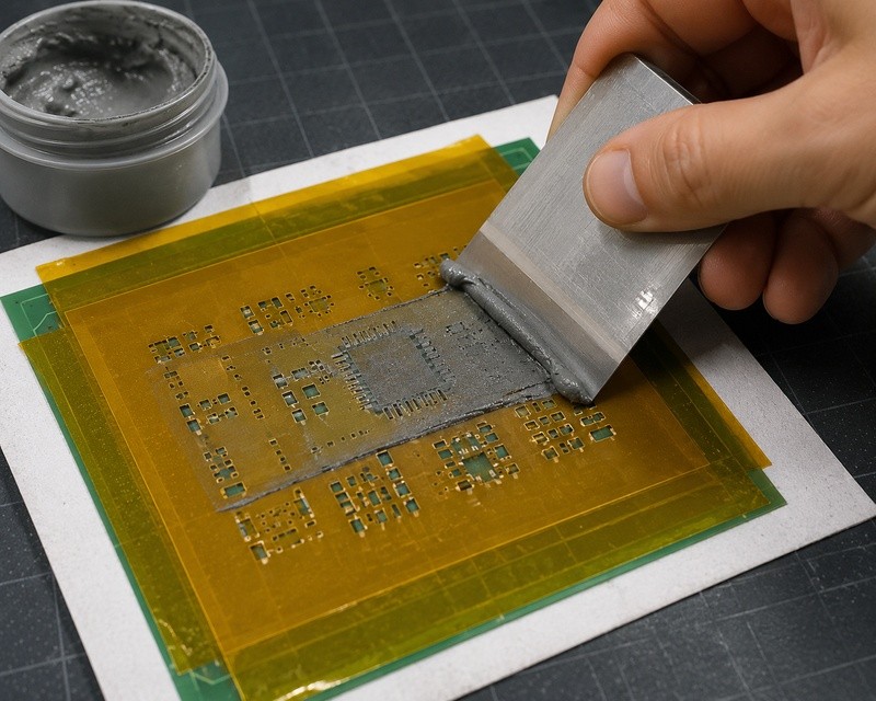
12.Print the solder paste.
Place a bead of conditioned solder paste above the apertures. Hold a squeegee at approximately 45–60 degrees and make one firm pass. Lift the PCB stencil vertically, then inspect every fine-pitch deposit before placing components.
How DIY PCB Stencils Are Made: Cutting Methods Compared
1Cut by Hand with a Craft Knife
Hand cutting is the least expensive process and only needs the use of a craft knife, cutting mat, and thin stencil material. It is suitable for SOIC packages, 0805 devices, DIP adaptors, and pads that are large in size or wide-spaced. The technique is the most effective when the pitch is around 1.27mm or larger.
The strengths of the technique include low costs and no need for special equipment. However, hand-cut apertures have inconsistent cuts, and it takes a long time to cut many holes. When it’s worth it: Hand cutting makes sense for one-off prototypes with only a handful of large pads.
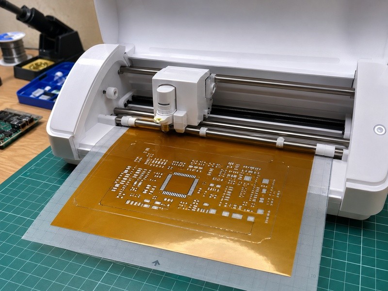
2Use a Vinyl or Craft Cutter (Cricut, Silhouette Cameo, Brother)
A Cricut, Silhouette Cameo, or Brother craft cutter can create a more repeatable stencil from Mylar, vinyl, or transparency film. This approach works well for 0402 and 0603 passives, SOIC packages, and some QFP components with a pitch of around 0.5 mm.
Craft cutters produce larger apertures cleanly and are faster than cutting by hand. However, blade depth, material movement, and corner rounding can affect accuracy. Most blade cutters struggle below approximately 0.5 mm pitch and may merge or distort tiny QFN and BGA apertures.
A Cricut PCB stencil or Silhouette Cameo PCB stencil is worthwhile when the machine is already available, and several simple boards need to be assembled. Test the blade depth and pressure on scrap material before cutting the final stencil.
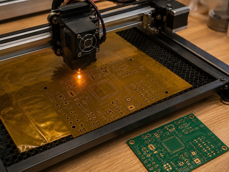
3Use a Laser Cutter (CO₂ / Diode / Fiber)
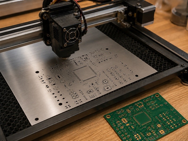
A laser-cut PCB stencil can provide finer and more consistent apertures than hand or blade-cut methods. The appropriate laser depends on the stencil material:
- A CO₂ laser can cut thin Mylar, PET, and Kapton film.
- A diode laser may cut some films but can melt or char Kapton.
- A fiber laser can cut thin stainless steel when the machine is properly configured.
As a typical starting point, a CO₂ laser may cut approximately 0.1 mm Mylar in one low-power pass. Kapton often requires careful adjustment of speed, power, focus, and ventilation to prevent darkened or raised aperture edges. Exact settings vary significantly by machine, lens, material, and laser wattage, so always test on scrap first.
DIY Stencil Comparison: Cost, Accuracy, Pitch, and Reuse
| Method | Cost | Accuracy | Best Pitch | Reusable | Difficulty |
|---|---|---|---|---|---|
| Craft knife | Under $10 USD if tools are owned | Low | About 1.27 mm or wider | One to a few boards | High for dense layouts |
| Vinyl or craft cutter | Low material cost; cutter required | Medium | About 0.5 mm in a tuned best case | Several boards | Medium |
| CO₂ laser cutter | Low at a makerspace; high to buy | Medium to high | About 0.5 mm practical | Several to a few dozen boards | Medium to high |
| Ordered steel stencil | From a few dollars depending on size, supplier, and shipping | High | Suitable for fine-pitch work, subject to DFM | Production-reusable | Low |
Common DIY PCB Stencil Mistakes
- Melted or charred aperture edges: If the openings have brown, rough, or raised edges, the laser is probably moving too slowly or using too much power. Increase the cutting speed, reduce the power, and test the settings on scrap material first.
- Too much solder paste: If paste forms blobs or bridges between nearby pads, the stencil material may be too thick or the apertures too large. Use thinner film and reduce the aperture dimensions.
- No aperture reduction: Fine-pitch openings copied at full pad size may deposit excessive paste and cause bridging. Reduce the aperture size by approximately 10–20% where appropriate.
- Poor registration or alignment: If the paste lands beside the pads or smears during lifting, the PCB or stencil is moving. Build a proper alignment jig, secure the board, and use a taped hinge for a controlled vertical lift.
- Using the wrong cleaning solvent: Acetone and other strong solvents can warp or cloud PET, Mylar, and similar films. Clean the stencil with isopropyl alcohol and test any cleaner on scrap material first.
For help identifying print-related problems, see the Solder Paste Printing Defects guide. The How to Use Solder Paste guide explains proper paste handling, application, and cleanup. For detailed squeegee technique, registration methods, and paste application best practices, refer to this SMT stencil printing practical guide.
The Limits of DIY Stencils: Where They Break Down
DIY PCB stencils work well for many prototypes, but their limits become clear as component size and board complexity increase.
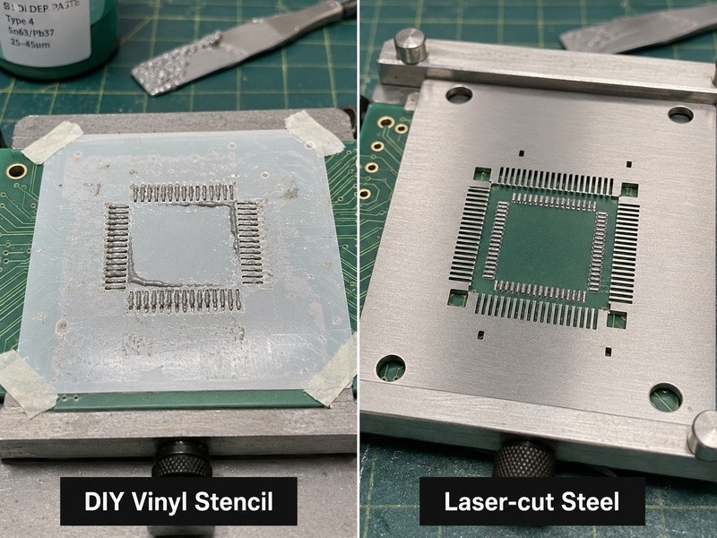
- Fine-pitch components are difficult: DIY methods are generally reliable down to about 0.5 mm pitch. Components such as 0.4 mm QFNs, fine-pitch QFPs, and BGAs often produce merged apertures, poor paste release, or solder bridges.
- Limited durability: Film and vinyl stencils usually last for approximately 5–30 prints. Repeated cleaning and squeegee pressure can stretch the material, tear aperture edges, or reduce accuracy.
- Inconsistent aperture quality and alignment: Hand-cut and diode-laser-cut openings may have rough, melted, or charred edges. Manual alignment also makes it difficult to achieve the same paste placement on every board.
- Poor control over thermal pads: DIY stencils are not well suited to creating precise window-pane aperture patterns for exposed QFN or DFN pads. A single large opening may deposit too much paste, causing components to float or solder voids.
- The process takes time: Exporting the paste layer, adjusting the design, testing cut settings, removing debris, and aligning the stencil can take significant effort, especially after every PCB revision.
DIY is still useful for simple prototypes and occasional builds. For fine-pitch parts, repeated assembly, or complex thermal pads, a professionally made stencil is usually the more dependable option.
Example: Why a DIY Stencil Failed on a 0.4 mm QFN
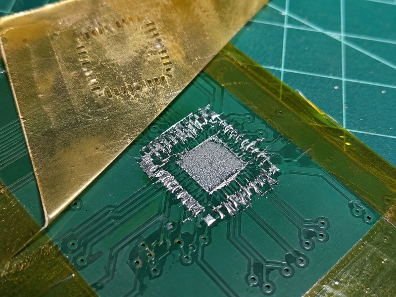
Consider a representative 0.4 mm QFN print. The solder paste looked even as the squeegee moved across the stencil. However, after lifting it, several lead apertures still held paste, the exposed-pad deposit smeared, and a bridge formed between two adjacent leads. The hot plate was not responsible because these defects appeared before reflowing.
The real issue was poor paste release. Rough or heat-glazed aperture walls gave the paste more surface to grip, while the untreated film lacked a low-adhesion surface. Smoother aperture walls reduce drag, and a non-stick coating improves paste transfer. This is why electropolishing and nano-coating can improve fine-pitch printing even when the paste, PCB, and reflow profile remain unchanged.
When Does It Make Sense to Order a Steel Stencil?
Order a Steel Stencil When:
- This is the second PCB revision, or you plan to build five or more boards.
- The design includes 0.5 mm or finer pitch, QFN, LGA, or BGA packages.
- An exposed thermal pad needs repeatable window-pane apertures.
- Paste volume must be consistent enough for inspection or production records.
- Cutting, weeding, and registering another homemade stencil will cost more than ordering one.
Keep Doing DIY When:
- You are validating one first-revision board and can tolerate manual inspection or rework.
- The smallest components are mostly 0805, 0603, SOIC, or other generous packages.
- You already own the cutter and can prepare the stencil quickly.
- Making the stencil is part of the experiment or learning process.
Professional laser-cut steel addresses the same release problem seen in the QFN example. Consistent aperture geometry improves transfer, electropolishing smooths the aperture walls, and optional nano-coating reduces paste adhesion. CAM processing can also optimize reductions and create window-pane thermal-pad openings.
See how to choose a solder paste stencil for guidance on foil thickness, frame type, and application.
JLCPCB is one example of the professional route, not the only possible supplier. Its current stencil service lists 304 HTA stainless steel, framed and frameless formats, Gerber and DXF support, cutting tolerances as tight as ±0.003 mm, and optional electropolishing, nano-coating, and step-stencil processing. See the full PCB PCB stencil manufacturing capabilities for detailed specifications on material grades, thickness options, and processing.
Today, a laser-cut stencil measuring up to 100 × 100 mm starts at approximately $3 USD. The fastest listed production time is 12 hours, although the final price and turnaround depend on the selected dimensions, processing options, order confirmation time, and delivery method. The stencil-ordering guide explains the file-upload and configuration process. After printing the paste, move directly to a controlled heating process. This guide to reflow soldering at home covers hot-plate and oven approaches.
FAQ about DIY PCB Stencils
Q:Can Printed Transparency Work Without Cutting Holes?
No. A normal inkjet- or laser-printed transparency only places an image on the film; solder paste cannot pass through it. You can use the printed transparency as a 1:1 guide for hand cutting or as artwork in a separate photo-etching process, but it is not a working transparency stencil by itself. Check printer scaling with a measured 10 mm test box before using any printed solder paste stencil template.
Q: Should the Bottom Paste Layer Be Mirrored?
It depends on how the cutter software defines the viewing side and how the physical stencil will be flipped during use. A top-side stencil is normally cut at 1:1 without mirroring when viewed from above the PCB. A bottom-side stencil may require mirroring because the sheet is turned over during printing. Add asymmetrical registration marks and test the orientation on paper before cutting the final film.
Q:Can I Reuse a Homemade PCB Stencil After Paste Dries?
Sometimes. But dried paste makes damage more likely. Soften the residue using IPA that is compatible with the film. Support the stencil on a flat surface and blot it with a lint-free wipe instead of scraping the aperture walls. Hold the cleaned stencil against a backlight and discard it if openings remain blocked, corners have curled, or narrow webs have stretched.
Q:Do I Need a Cutting Mat for a Cricut or Silhouette Stencil?
Usually, yes. A clean, low-tack cutting mat holds thin Mylar or polyimide flat while the blade changes direction. A worn, highly flexible, or excessively sticky mat may cause trouble because the sheet can move during cutting or stretch during removal. Tape the outside border, keep the tape away from active apertures, and verify both the X and Y scale with a test square before cutting the final PCB stencil.
Q:Does Lead-Free Paste Need a Different DIY Stencil?
Not simply because it is lead-free. Stencil geometry is determined mainly by pad size, component pitch, desired paste volume, foil thickness, and paste-release behavior. Lead-free pastes can differ in viscosity and powder size, so the same aperture may print differently. Condition the paste according to its technical data sheet, perform a test print, and adjust the aperture or printing process according to the deposit rather than the alloy label alone.
Q:How Should I Store Kapton or Mylar Stencils?
Store each stencil flat between two smooth protective sheets rather than rolling or folding it. Label the PCB revision, board side, material thickness, and orientation. Remove all paste before storage and keep the package away from heat, moisture, sharp tools, and heavy objects. A clean, flat stencil is easier to align on the next build and less likely to produce uneven deposits.
Conclusion: Making Your DIY PCB Stencil
A DIY PCB stencil is a useful maker skill and is often the fastest solution for one larger-part prototype. Export the correct paste layer, preserve the 1:1 scale, test the cutter on scrap, use a rigid registration jig, and judge success by the paste left on the pads. Once you hit fine pitch, repeat quantity, or exposed thermal pads, an ordered laser-cut steel stencil is usually easier and cheaper than another round of DIY tuning.
Cut your own stencil when it suits the project, and order one when precision and repeatability matter more.
Keep Learning
DIY PCB Stencil: How to Make a Solder Paste Stencil
Key Takeaways DIY is possible: You can make a working solder paste stencil from Kapton, Mylar, or vinyl using a craft knife, vinyl cutter, or laser for larger SMD components and low-volume prototyping. 0.5 mm pitch is the practical boundary: DIY stencils work well above 0.5 mm pitch but struggle with finer QFNs, QFPs, and BGAs due to poor aperture quality and paste release. Match thickness to your smallest pad: Use 0.10–0.15 mm (4–6 mil) sheet stock, choosing thinner material for smaller pads and thic......
How to Choose an SMT Stencil
What is an SMT stencil? SMT Stencil is a thin metal sheet used in the soldering process for SMT (Surface Mount Technology) and it plays an essential role in the SMT soldering process. Smt Stencil allows the direct placement of solder paste onto the SMD pads of PCB, which can help prevent errors and defects during the reflow soldering process. This results in a precise amount of tin coverage once the work is completed. Types of SMT Stencils Depending on the application of solder paste, there are three ......
Order Custom Stencils for PCB Assembly: How to Make, Buy, and Choose the Right Supplier
Surface Mount Technology (SMT) stencils are essential tools in modern PCB assembly. They are thin sheets of metal, usually stainless steel, with precise cut-outs that allow solder paste to be applied accurately to PCB pads. The quality of the stencil directly affects solder paste deposition, which in turn impacts the reliability of the final assembled PCB. Engineers often need to order custom stencils instead of relying on generic options. Every PCB design has unique pad layouts, component densities, ......
Custom Stencils for PCB Assembly: Design, Ordering, and Usage Guide
Have you ever faced solder bridging or insufficient solder issues that ruined an entire production batch? In many cases, the problem is not the pick-and-place machine, but the very first step of the process: solder paste printing. This is where custom stencils make the difference between a reliable product and one that requires extensive rework. Unlike rigid standard stencils, a custom SMT stencil gives engineers full control over solder paste volume, allowing precise adjustment to match increasingly ......
SMT Stencil Thickness Guide 2026: How to Choose the Right Solder Paste Stencil
In SMT assembly, the stencil quietly decides whether a production run succeeds or fails. Problems like bridging, tombstoning, and insufficient wetting are frequently traced back not to PCB design errors, but to incorrect stencil selection or poorly controlled paste volume. Quick Answer: How to Choose a Solder Paste Stencil If you need to define your stencil parameters immediately, follow this quick decision guide: Select thickness based on component pitch: Use component density as your primary baselin......
Custom Cut Stencils for PCB Assembly: How to Cut, Use and Choose the Right PCB Stencil
Custom-cut stencil and Solder paste printing are two of the most vital processes in Surface Mount Technology (SMT) PCB assembly, concerning solder joint quality, electrical performance, and product reliability over time. SMT stencils are used to deposit solder paste in accurate amounts onto PCB pads, or for depositing and compressing adhesive pastes which are arranged in the form of a column on components such as connectors and sockets. While PCB designs have seen a trend toward increased density, fin......