
Custom Stencils for PCB Assembly: Design, Ordering, and Usage Guide
6 min
- What Is a Custom SMT Stencil?
- What Can Be Customized in an SMT Stencil?
- How to Make or Order a Custom SMT Stencil
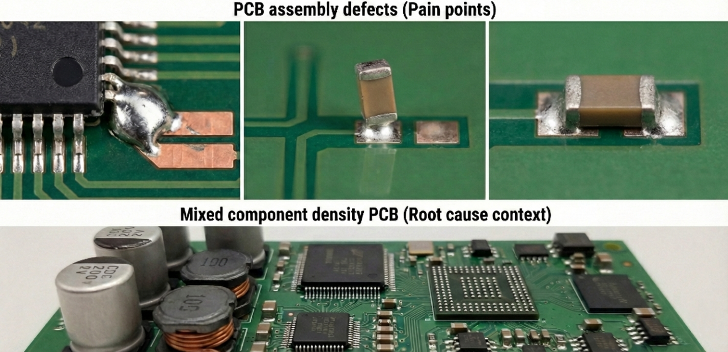
Have you ever faced solder bridging or insufficient solder issues that ruined an entire production batch? In many cases, the problem is not the pick-and-place machine, but the very first step of the process: solder paste printing. This is where custom stencils make the difference between a reliable product and one that requires extensive rework. Unlike rigid standard stencils, a custom SMT stencil gives engineers full control over solder paste volume, allowing precise adjustment to match increasingly dense and challenging PCB layouts.
This article explains what custom SMT stencil is, what aspects can be customized, and how to make or order a customized stencil effectively.
What Is a Custom SMT Stencil?
Basic Definition & Purpose
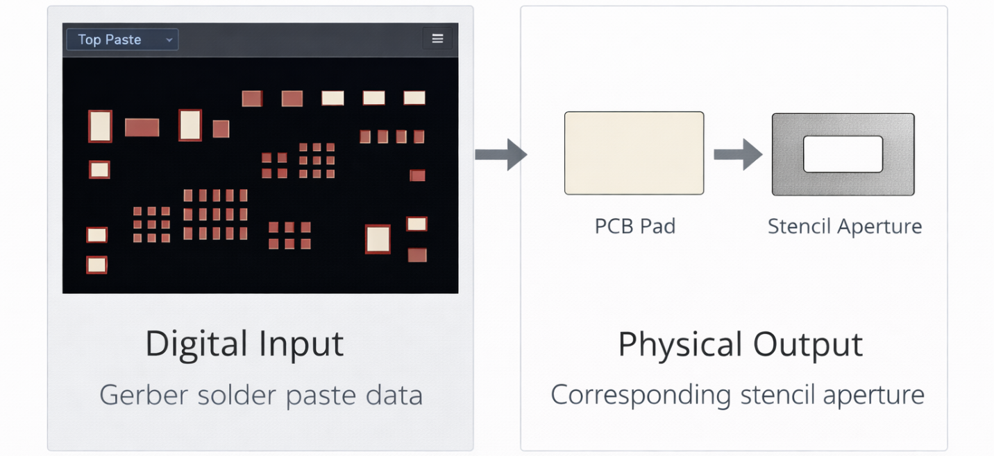
A custom SMT stencil is a precision sheet—typically made of stainless steel—that is specifically designed to match the unique pad layout of a particular PCB, rather than using a standard stencil size or generic design. The stencil apertures are manufactured to closely follow the PCB pad design, while other parameters such as thickness and material can be adjusted to suit assembly requirements.
The primary purpose of using a custom stencil is to control solder paste deposition accurately, ensuring consistent and reliable solder joints throughout the SMT assembly process.
Why Customization Matters for PCB Assembly
Customization becomes especially critical for PCBs that use fine-pitch ICs, QFN packages, BGAs, or a mix of different component sizes. In such cases, a standard stencil may deposit too much or too little solder paste, leading to defects such as solder bridging, tombstoning, or insufficient solder joints.
By using a customized stencil, engineers can optimize solder paste volume for each pad type, improving process stability and enhancing long-term product reliability.
Industry Standards and Technical Ratios (IPC-7525)
To produce a high-quality custom SMT stencil, the design cannot be arbitrary. The industry follows the IPC-7525 standard
to determine whether solder paste will be released cleanly from the stencil or remain trapped inside the apertures. Two key calculations are commonly used:
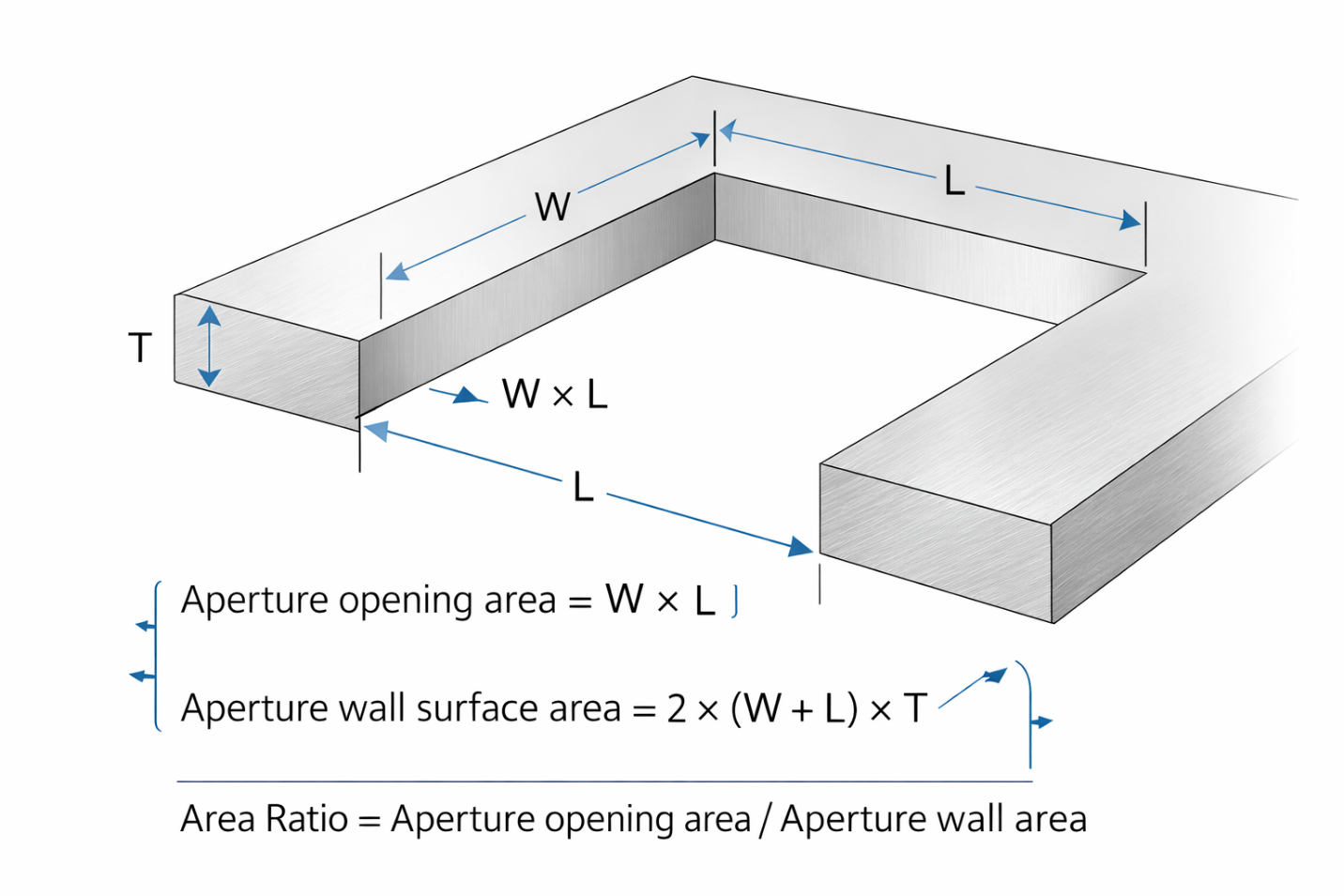
1. Aspect Ratio: The ratio between the smallest aperture width and the stencil thickness. The recommended value is greater than 1.5.
2. Area Ratio: The ratio between the aperture opening area and the total aperture wall area, which can be expressed as:
Area Ratio = (Aperture Area) / (Aperture Wall Height × Aperture Perimeter)
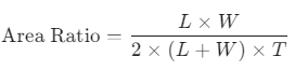
(Where L = length, W = width, and T = stencil thickness).
Ideally, this value should be greater than 0.66 to ensure efficient solder paste transfer to the PCB.
What Can Be Customized in an SMT Stencil?
Stencil Size, Thickness, and Material
One of the most common customization options is stencil size. A custom stencil can be designed to match specific PCB dimensions or panel configurations, whether for prototyping or full-scale production.
Stencil thickness is another critical parameter. Thicker stencils deposit more solder paste, while thinner stencils are typically used for fine-pitch components to reduce the risk of solder bridging. Stainless steel is the most widely used material due to its high durability and compatibility with laser cutting processes.
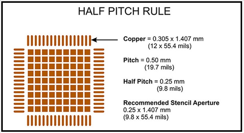
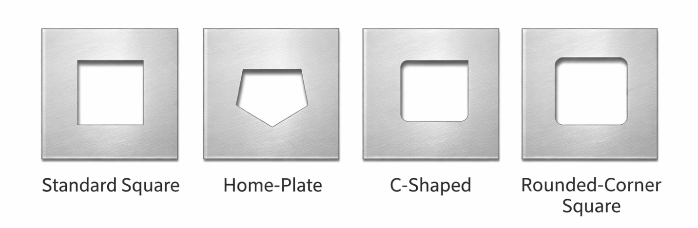
Aperture Modifications and Fine-Pitch Options
Aperture design is a crucial part of custom stencil fabrication. Apertures are often not made the same size as the PCB pads, but instead modified to control solder paste volume.
Common aperture customization techniques include:
· Aperture size reduction for fine-pitch pads
· Modified aperture shapes for QFN and BGA packages
· Different aperture designs within a single stencil for mixed-component PCBs
These approaches help ensure stable solder paste release and consistent reflow results.
Framed, Frameless, and Nano-Coating Choices
Custom SMT stencils are available in various configurations. Framed stencils are typically used in automated SMT production lines, while frameless stencils are more common for manual printing and prototyping.
Additional options such as nano-coating are also available. Nano-coated stencils reduce solder paste adhesion to aperture walls, improving paste release efficiency and reducing the frequency of stencil cleaning. This option is particularly useful for enhancing the performance of customized stencils in assembly processes that demand high consistency.
How to Make or Order a Custom SMT Stencil
File Requirements (Gerber, CAD)
To create a custom SMT stencil, accurate design files are required. Most stencil manufacturers accept Gerber files generated from PCB design software. These files define pad locations, sizes, and shapes that form the basis of the stencil apertures.
Some service providers also support direct CAD data or integrated stencil layers, making the ordering process more efficient and reducing the risk of design errors.
Local vs Online Options
Engineers can choose between local suppliers and online services when ordering custom stencils. Searching for a custom stencil near me can offer advantages such as direct communication and faster support, especially for urgent prototyping needs.
On the other hand, custom stencils online services provide greater convenience, competitive pricing, and integration with PCB manufacturing services. Online platforms typically allow direct file uploads and quick configuration of stencil parameters.
Step-by-Step Ordering Process
Understanding the ordering workflow is important to minimize design errors. Below is a typical step-by-step guide when ordering custom stencils online through JLCPCB:
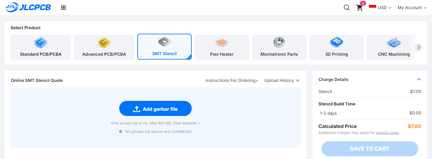
1. Upload Design Files: Upload your PCB Gerber files. The JLCPCB system automatically detects solder paste layers (Top/Bottom Paste).
2. Select Stencil Type (Framework): Choose Non-framework for manual soldering or if you already have a universal frame. Select Framework for automated SMT stencil printers.
3. Nano-Coating Option (New Feature): Nano-coating is highly recommended for fine-pitch designs. This hydrophobic layer prevents solder paste from sticking to aperture walls, producing sharper prints and reducing cleaning frequency.
4. Select Stencil Side: Choose whether you need Top, Bottom, or Both sides, depending on where SMT components are placed.
5. Choose Custom Size: For small PCBs, specifying exact dimensions (e.g., 100 × 100 mm) can help reduce cost and storage space.
6. Set Stencil Thickness: Common options are 0.12 mm and 0.15 mm. Use 0.12 mm for designs with many fine-pitch components such as 0.5 mm-pitch ICs.
7. Electropolishing Option: Electropolishing smooths aperture walls, further improving solder paste release.
8. Fiducials (Reference Marks): Select No Fiducial for manual use. Choose Etched Half into Board for automated machines to assist camera alignment without fully cutting through the metal.
9. Review and Checkout: Review all selected parameters, confirm shipping details, and submit your order.
Using custom stencils is an effective solution for improving solder paste printing accuracy and overall SMT assembly quality. By customizing stencil size, thickness, material, and aperture design, engineers gain better control over solder paste deposition and can significantly reduce assembly defects.
Whether ordering a custom SMT stencil from a local supplier or through custom stencils online services, selecting the right stencil solution plays a critical role in achieving stable, efficient, and high-quality PCB assembly processes.

Keep Learning
SMT Stencil Cleaning Guide: Process, Frequency, and Tips
Key Takeaways about SMT Stencil Cleaning SMT stencil cleaning removes solder paste residue from aperture walls and the stencil underside, keeping paste transfer efficiency between 80% and 100%. Industry analysis attributes over 60% of SMT defects to the paste-print step — most of which trace back to a stencil cleaning lapse. Two stages matter: under-screen cleaning (between cycles, typically every 5–10 prints) and off-line cleaning (after production completes). IPA handles standard flux residue; dedic......
Top 5 Circuit Board Stencil Mistakes & How to Fix Them for Higher SMT Yield
Usually, the circuit board stencil is responsible for roughly 60% to 70% of all SMT defects. That number surprises people. It shouldn't. The stencil controls paste volume, deposit geometry, and positional accuracy all at once. When it gets wrong, everything downstream pays for it. The shift in thinking that separates good engineers from great ones is simple: stop seeing the PCB stencil as a metal sheet with holes in it. It is a precision fluid delivery system. Every aperture wall, every micron of foil......
How to Apply SMD Glue Using SMT Stencils (Design, Thickness & Troubleshooting Guide)
The reality of modern PCB assembly is that "mixed-technology" is still very much the norm. When a board hits the wave soldering machine, bottom-side SMD components face a high-velocity river of molten metal. Without a solid mechanical bond, they’ll simply wash away into the solder pot. That’s where the precision application of SMD glue becomes the difference between a successful run and a bin full of scrap. Quick Answer: How to Apply SMD Glue in SMT If you need to configure your SMT stencil for adhesi......
The Essential Guide to SMT Stencils in PCB Assembly
Introduction In the dynamic world of electronics manufacturing, Surface Mount Technology (SMT) plays a crucial role in achieving efficiency and precision in printed circuit board (PCB) assembly. Central to the SMT process is the SMT stencil, an indispensable tool for the accurate application of solder paste. This ensures solid electrical connections between components and PCBs. This guide delves into the specifics of SMT stencils, examining their types, materials, manufacturing methods, advantages, ch......
Nano-Coatings in PCB Manufacturing: How They Outperform Traditional Stencils
Nano coating is a thin hydrophobic (water repellent) and oleophobic (oil repellent) treatment used on the undersides and edges of solder paste stencils. With this the surface becomes non-stick which reduces the number of cleaning cycles required for the solder paste printing process. Upon application, the less than 5 nanometer coating bonds with the stencil foil at the microscopic level, which does not change the size and shape of the stencil. Nano coating is an industry proven process which shows imm......
How to Choose an SMT Stencil
What is an SMT stencil? SMT Stencil is a thin metal sheet used in the soldering process for SMT (Surface Mount Technology) and it plays an essential role in the SMT soldering process. Smt Stencil allows the direct placement of solder paste onto the SMD pads of PCB, which can help prevent errors and defects during the reflow soldering process. This results in a precise amount of tin coverage once the work is completed. Types of SMT Stencils Depending on the application of solder paste, there are three ......