How to Generate Gerber Files in Altium Designer 26 [Updated]
Last updated on Sep 28, 2026

Note
This guide was created using Altium Designer 26.1.1. The menu paths, the Gerber Setup dialog, and the NC Drill Setup dialog are unchanged in Altium Designer 24 and 25, so the same procedure applies to those versions.
Exporting Altium PCB to Gerber files looks like two menu clicks, until your order goes on hold because the drill file never made it into the ZIP or the board outline plotted to a mechanical layer nobody reads.
This guide walks through the full export on a real two-layer USB Power Delivery board, from layer selection to the finished archive.
In this guide, you will learn:
- Which layers to plot in the Gerber Setup dialog
- Correct units, decimals, and advanced Gerber settings
- How to generate NC Drill files for plated and non-plated holes
- Where Altium writes the output files on your drive
- How to package everything into one upload-ready ZIP
Altium Gerber Export: What to Check Before You Start
Gerber export is the last step of design, not the first step of manufacturing. Anything wrong in the PCB document is copied faithfully into the Gerber set, so the board has to be clean before you open the export dialog.
The example used throughout this guide is a two-layer USB Power Delivery board with dimensions of 18.54 x 32.64 mm.
PCB Design Rule Setup for JLCPCB Capabilities
Before exporting, confirm the following:
- Your design rules match the JLCPCB PCB capabilities for minimum track width, clearance, hole size and annular ring.
- Go to Tools > Design Rule Check runs clean, with no unresolved violations.
- All copper, silkscreen and mask objects sit inside the board outline.
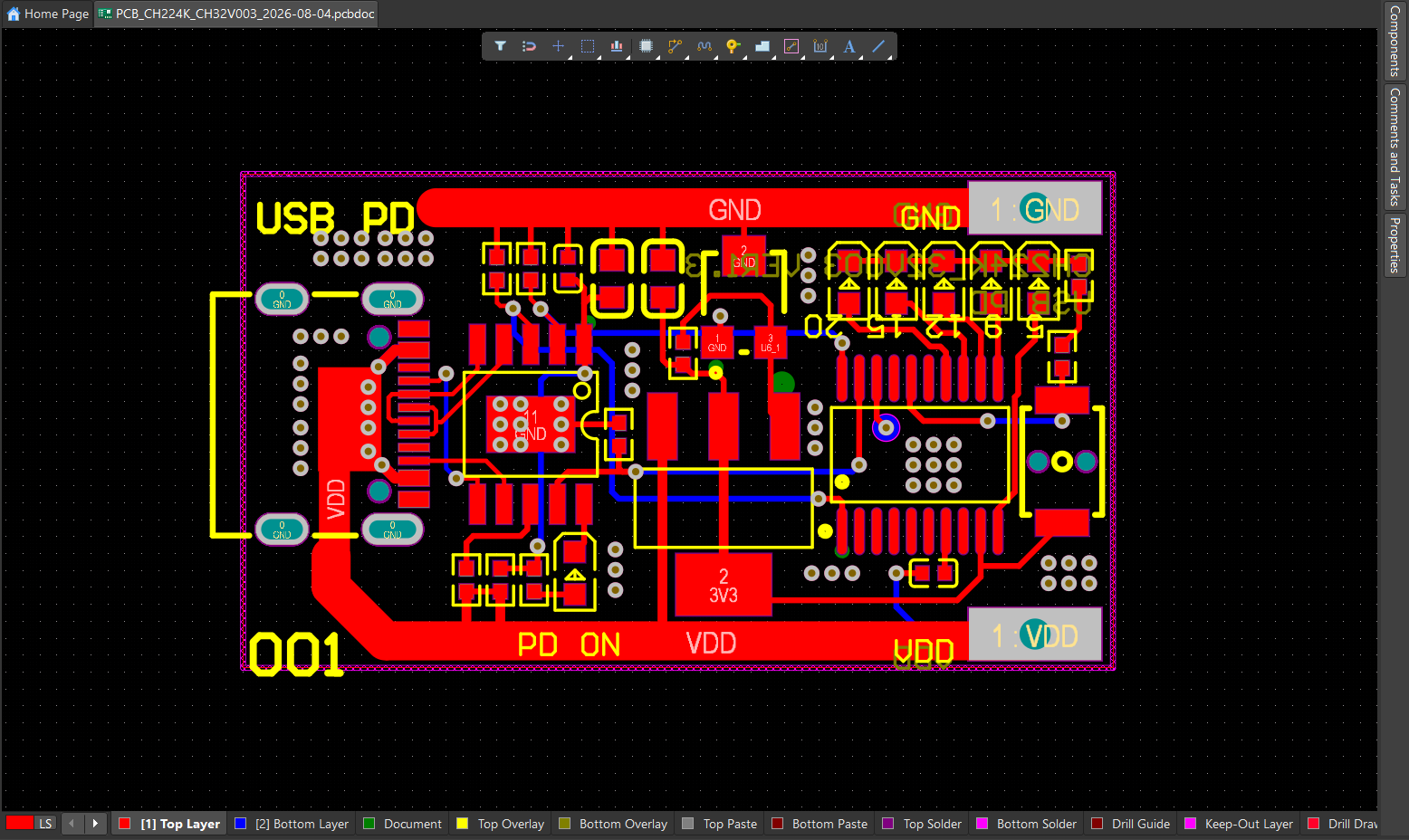
Figure 1. The example two-layer USB Power Delivery board opens in the Altium PCB editor
Important: A Gerber file records exactly what is on the layer, including a designator sitting on top of a pad or a silkscreen line crossing a mask opening. Fix those in the PCB editor, not in the exported files.
Altium Gerber Files: Required Layers and File Extensions
A complete Gerber set for a two-layer board is ten files: two copper, two silkscreen, two solder mask, two paste mask, one board outline, and the NC drill data. Altium names them with Protel extensions, which JLCPCB reads directly.
| Layer in Altium | Gerber Extension | What It Controls |
|---|---|---|
| Top Layer | .GTL | Top copper: tracks, pads, polygons |
| Bottom Layer | .GBL | Bottom copper |
| Inner Layer 1 / Inner Layer 2 | .G1 / .G2 | Inner copper on 4-layer boards and above |
| Top Overlay | .GTO | Top silkscreen legend |
| Bottom Overlay | .GBO | Bottom silkscreen legend |
| Top Solder | .GTS | Top solder mask openings |
| Bottom Solder | .GBS | Bottom solder mask openings |
| Top Paste | .GTP | Top stencil apertures, used for assembly |
| Bottom Paste | .GBP | Bottom stencil apertures |
| Board Outline | .GM | Board profile: the shape and size that gets routed |
| Keep-Out Layer | .GKO | Alternative outline source; include only if no .GM profile is plotted |
| NC Drill, plated and non-plated | .TXT (Excellon) | Hole positions, diameters and plating |
How to Generate Gerber Files in Altium Designer: Step by Step
Summary
The full Gerber export is five steps:
- Open File > Fabrication Outputs > Gerber Files with the PCB document active.
- Set Units to Millimeters and Decimal to 0.0001 mm.
- Tick the copper, silkscreen, mask, paste and board outline layers in Layers to plot.
- Set the Advanced tab for RS-274X output.
- Click Apply, then review the result in the CAMtastic viewer.
Step 1: Open Fabrication Outputs and Select Gerber Files
Open the .PcbDoc file you want to manufacture so it is the active document, then choose File > Fabrication Outputs > Gerber Files. The Gerber Setup dialog opens.
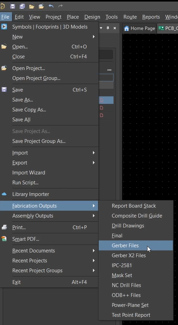
Figure 2. Gerber Files opens the Gerber Setup dialog, use Gerber Files, not Gerber X2 Files.
Step 2: Set Gerber Units, Decimal, and File Name Format
The left-hand column of the Gerber Setup controls the coordinate resolution and the output file names. Set it as follows:
- Units: Millimeters
- Decimal: 0.0001 mm (a 4:4 coordinate format, giving 0.1 micron resolution)
- Outputs: FileName.Extension: select the filename.* option so the export produces .gtl, .gbl, .gto and the rest, rather than a folder of identically named .gbr files
- Include unconnected mid-layer pad: ticked
- Generate Reports: ticked
- Merge regions and pads inside Footprint: left unticked
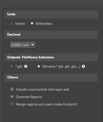
Figure 3. Units set to Millimeters, Decimal set to 0.0001 mm
Note: The NC Drill Setup dialog in the next section stays on Inches and 2:5, even though the Gerber files are in millimeters. Mixing the two is safe, because every Excellon drill file declares its own units in its header (INCH and FILE_FORMAT=2:5 in this example), so the CAM system never has to guess.
Step 3: Select the Layers to Plot in Gerber Setup
Open the Layers to plot tab. Altium groups the available layers by function and shows the exact file name each one will produce.
Tick these groups:
- Board Outline (.GM)
- Copper Layers: Top Layer (.GTL) and Bottom Layer (.GBL)
- Silkscreen: Top Overlay (.GTO) and Bottom Overlay (.GBO)
- Solder Mask: Top Solder (.GTS) and Bottom Solder (.GBS)
- Paste Mask: Top Paste (.GTP) and Bottom Paste (.GBP)
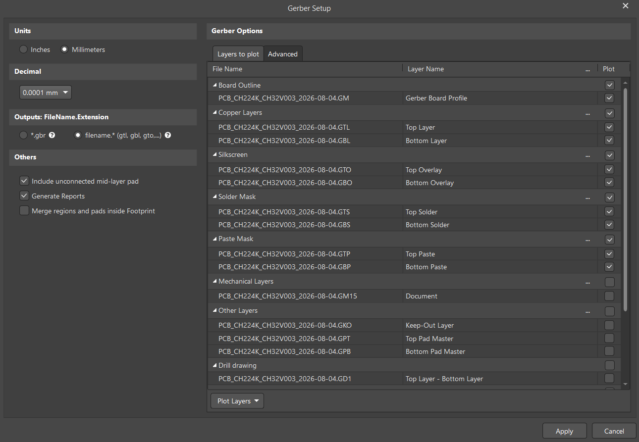
Figure 4. Board Outline, copper, silkscreen, solder mask and paste mask are ticked.
Step 4: Configure Advanced Gerber Settings for RS-274X Output
Switch to the Advanced tab. These settings control how the coordinate data is written, and the defaults shown below are correct for JLCPCB:
- Aperture Tolerances: Plus 0.00013mm, Minus 0.00013mm
- Leading/Trailing Zeros: Suppress leading zeroes
- Plotter Type: Unsorted (raster)
- Others: Optimize change location commands ticked
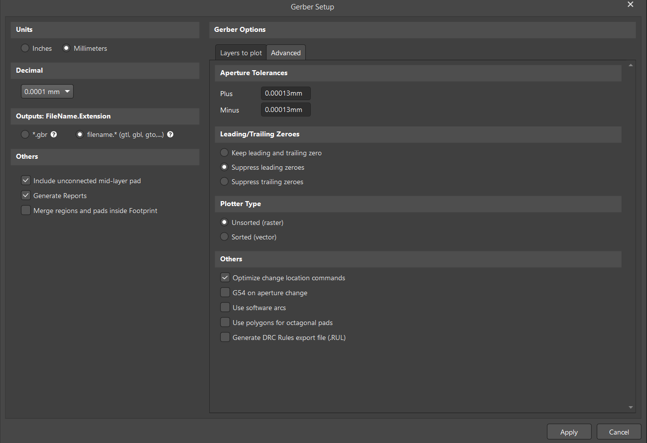
Figure 5. Advanced Gerber settings
Leaving Use software arcs unticked keeps true arc commands in the file instead of breaking curves into line segments, which produces smaller files and cleaner routed edges.
Click Apply to run the export.
Step 5: Review the Gerber Output in CAMtastic
Altium generates the Gerber files and immediately opens them in CAMtastic, its built-in Gerber viewer, as a new .CAM document. Use it as a first sanity check: the composite render should show the board with its outline, copper, pads and silkscreen in the right places.
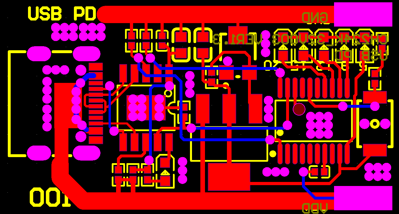
Figure 6. The exported Gerber set rendered in CAMtastic
Close the .CAM document without saving once you have checked it. Saving creates an extra CAM file in the project that has no role in fabrication.
The generated Gerber files now sit in the project output folder, one file per plotted layer, all sharing the PCB document name.
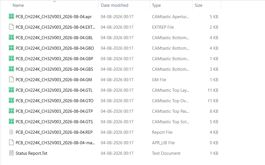
Figure 7. The Gerber output from Altium
How to Generate NC Drill Files in Altium Designer
Gerber files describe copper, mask, and legend. They contain no hole data at all. Export holes separately as NC Drill files in Excellon format; skipping this step is the most common reason an order is held.
Step 1: Open Fabrication Outputs and Select NC Drill Files
With the same PCB document active, choose File > Fabrication Outputs > NC Drill Files.
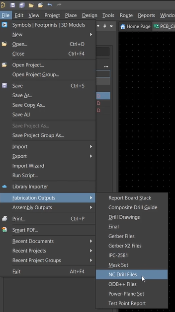
Figure 8. File → Fabrication Outputs → NC Drill Files opens the NC Drill Setup dialog.
Step 2: Set NC Drill Units, Format, and Zero Suppression
Configure the NC Drill Setup dialog as follows:
- Units: Inches
- Format: 2:5, which gives 0.01 mil resolution
- Leading/Trailing Zeroes: Keep leading and trailing zeroes
- Coordinate Positions: Reference to absolute origin
- Optimize change location commands: ticked
- Generate separate NC Drill files for plated & non-plated holes: ticked
- Generate separate NC Drill files for VIA Features: unticked
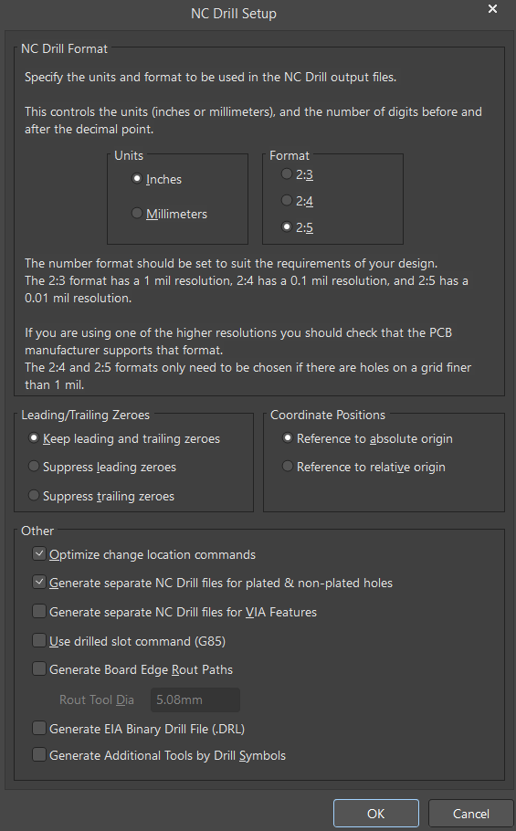
Figure 9. NC Drill Setup in Altium
Click OK. Altium may show an Import Drill Data dialog next; accept the defaults to render the result.
Step 3: Review the NC Drill Output
The drill data opens in CAMtastic as a hit map. Compare it against the board: every pad and via should have a hit, mounting holes should be present, and nothing should sit outside the outline.

Figure 10. The NC drill output rendered as hits.
This export produces three drill files plus a drill report. If a drill file is ever rejected because its tool list cannot be read, see Manually Adding a Tool List for a Drill File.
How to Package Altium Gerber Files Into a ZIP for JLCPCB
Altium Designer writes fabrication output to a Project Outputs for <ProjectName> folder created inside your project directory, next to the .PrjPcb file. Both the Gerber set and the NC drill set are in the same folder, so there is only one place to collect files.
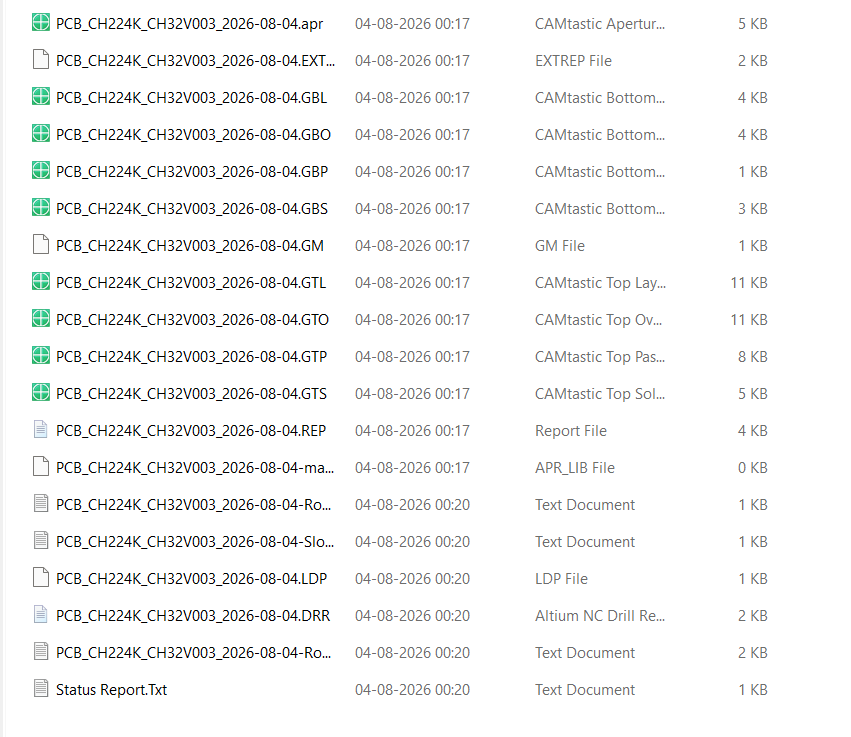
Figure 11. The complete output folder after both exports: the Gerber and the NC drill files
Select the files, right-click, and compress them to a .zip file.
JLCPCB accept archive types are .zip and .rar only, and the structure must be flat, with the files at the top level rather than inside a nested subfolder.
Upload Your Altium Gerber ZIP to JLCPCB
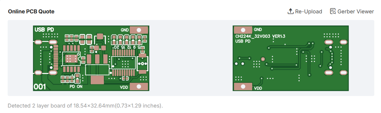
Figure 12. Reporting a detected 2-layer board of 18.54 x 32.64 mm.
FAQs
How do I export Gerber files from Altium Designer?
Open the PCB document, choose File > Fabrication Outputs > Gerber Files, set Units to Millimeters and Decimal to 0.0001 mm, tick the copper, silkscreen, mask, paste and board outline layers, configure the Advanced tab, then click Apply. Run NC Drill Files afterward for the hole data.
What is the difference between Gerber and NC Drill files?
Gerber files are 2D image files describing copper, solder mask, silkscreen and paste on each layer. NC Drill files are Excellon machine files listing hole coordinates, diameters and plating. Neither replaces the other, and a board cannot be manufactured unless both are in the archive.
Does JLCPCB accept Gerber X2 from Altium?
No. The accepted format is RS-274X, extended Gerber with embedded apertures. Use the Gerber Files entry in the Fabrication Outputs menu, not Gerber X2 Files. X2 embeds extra layer attributes that are not required, and files exported that way may be rejected at CAM review.
Where does Altium Designer save the Gerber output?
In a Project Outputs for <ProjectName> folder created inside your project directory, alongside the .PrjPcb file. Both the Gerber set and the NC drill files are written there. The drill files carry a later timestamp because the two exports are run as separate steps.
Why is my board outline missing from the Gerber files?
Either the Board Outline was unticked in Layers to plot, or the outline was drawn on a mechanical layer that was not plotted. Tick the layer that actually carries the outline, plot only one outline layer, and confirm the shape is closed before re-exporting.