
Why Tolerance Analysis Is Key to Reliable and Cost-Effective PCB Production
12 min
- Understanding Tolerance Analysis in PCB Manufacturing
- Primary Areas Where Tolerance Analysis Matters Most
- Common Tolerance Analysis Methods and Tools
- Benefits of Thorough Tolerance Analysis
- JLCPCB's Professional Approach to Tolerance Analysis
- FAQ abouot Tolerance Analysis
- Conclusion
Key Takeaways
- Tolerance analysis bridges CAD perfection and manufacturing variations to ensure reliable PCB assembly.
- Focus on critical areas: annular rings, hole tolerances, trace/space, layer registration, and solder mask alignment.
- Apply Worst-Case, RSS, or Monte Carlo methods for effective tolerance stack-up.
- Proper analysis boosts yield, cuts respins and costs — start with JLCPCB’s DFM review.
Have you ever sent a board to fabrication, which appeared flawless on the computer screen, but then found the parts didn't fit? Perhaps the press-fit connector wouldn't fit, or the fine-pitch QFN may have been landed a bit off target. I've been there, and almost every time, the primary cause is tolerance analysis. The CAD model is mathematically accurate, but the factory is not. In no way is there a perfect manufacturing process that will create an exact replica of your design files. The holes are a little bigger or smaller, the copper is a little thicker or thinner, and there are some microns of movement between the layers in the lamination process. These deviations are all very small, but they add up.
If you don't pay attention to how they are added up, you will get boards that are technically “in spec” but not able to assemble. In this blog, I'd like to guide you through what tolerance analysis is, how it applies to a PCB, and the 3 primary ways engineers predict the worst. A modern fabricator will also be examined, and how he or she approaches the problem to ensure your design comes across flawlessly from screen to reality. Let's dig into it.
Understanding Tolerance Analysis in PCB Manufacturing
What Tolerance Analysis Is and Its Purpose
Tolerance analysis is the art of determining how tolerances, or variations, of each individual component add up to impact the finished assembly. Each dimension of your PCB (a drill hole, trace width, pad position, etc.) has a range of deviation that it can have without causing problems, and these are known as tolerances. The fabricator assures you that the feature will be within that range, but not at the nominal.
It is a very effective and simple objective. You want to make sure that your board can still function mechanically and electrically, even if all of the deviations were to go against you. This means that a connector still connects, a via still lands within its annular ring, and a controlled-impedance trace still achieves its target. To sum up: Tolerance analysis is engineering without the guesswork. You don't have to cross your fingers and hope that your tight tolerances make it through production; you know they will. This is the gap between a design that has 99% and 70%.
The Relationship Between Design Tolerances and Production Reality
You love your CAD tool and are happy to create a 0.20 mm trace and 0.15 mm gap. Well, on paper, it is okay. However, there is a real-world etching tolerance, and the copper can be etched narrower or wider than drawn, using up the etching tolerance. There is the same difference between the hole you will end up with and the diameter of your drill. Drilled holes are plated to reduce the finished hole size and, of course, the drill bit wears with every hit it takes, thousands of times. Production reality is always moving; your nominal numbers never see it. Great designers add margins to their files because they know about the margin. Tolerance analysis is the method of quantifying that margin rather than guessing.
Primary Areas Where Tolerance Analysis Matters Most
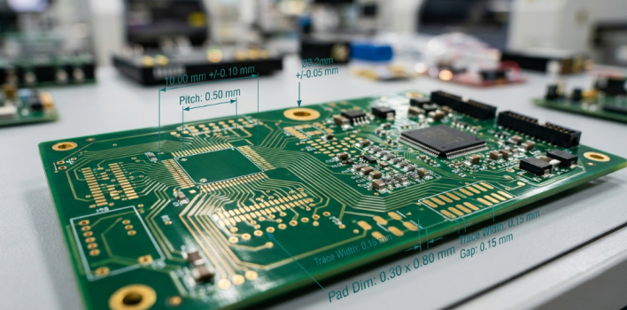
Hole Sizes, Pad Dimensions, and Trace Width Control
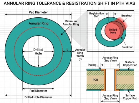
Certain features are much more susceptible to change than others. A typical example of this is a hole made by drilling, where a fabrication tolerance of + or - 0.05mm to + or - 0.1mm is common, depending on the type of hole and the plating. If you don't do this, a press-fit pin or a very close tolerance mounting hole (used in a number of cases) can fail. The next critical area is the annular ring. The copper collar that surrounds a drilled hole is called the annular ring and should remain above the minimum even when the drill wanders, and the layers move. When the pad is too small and the hole drills off-center, you'll end up with a breakout at the edge of the pad, where the hole meets the pad. On high-density and impedance-controlled designs, trace and space are of utmost importance. These are the features I would always look for first:
- Drill to copper clearance, which may collapse due to drill wander.
- An annular ring that has the potential to break out under registration error
- Trace width for sensitivity to etch tolerance for controlled impedance
- The most restrictive spacing between traces for etching is required.
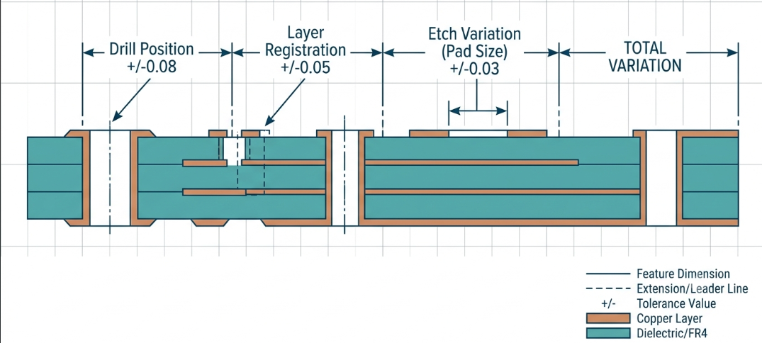
Layer Registration, Copper Thickness, and Solder Mask Alignment
Multilayer boards introduce an additional, completely new dimension: the way the layers match up. Layer-to-layer registration indicates the positioning precision of each copper layer in a layered structure, and poses a direct threat to buried vias and inner-layer annular rings. There is also a tolerance for Copper Weight. There is a range of actual thickness for a nominal 1 oz copper finish; the final copper plating on the exterior layers can be significantly different and change impedance and current capacity.
Pushing high currents means that copper-weight tolerance should be a real calculation. Lastly, solder mask registration determines the accuracy of the solder mask openings in relation to your pads. A misregistered mask can invade a pad or expose copper next to a pad, leading to solder bridging on fine pitch parts.
Common Tolerance Analysis Methods and Tools
Worst-Case, RSS, and Monte Carlo Approaches
There are three primary methods for tolerance analysis, and the one used will depend on the level of conservatism desired. Both handle the set of deviations differently.
- Worst-Case analysis is simply the addition of all extremes of tolerances in the same direction. It assumes all the features deviate at their extreme limits at the same time (the worst-case scenario). It ensures that the design never fails, yet it may be too conservative and may impose unnecessary and costly tight tolerances.
- The midpoint between extremes is RSS (Root Mean Squared Error). When a number of tolerances are added together, it does not use the sum of those tolerances, but rather the square root of the sum of the squared tolerances, under the assumption that all variations are normally distributed. It shows the truth that most of the time, no feature is at its extremes at the same time, providing you with a more realistic combination at a given confidence level.
- The Monte Carlo simulation method is a random sampling method. The software randomizes a number for each dimension, from its distribution, constructs a virtual board, and does it thousands of times to map the actual distribution of results. The most flexible and accurate, particularly for non-normal distribution, but requires good data and tooling.
Using Tolerance Stack-Up Analysis for Critical Features
If one dimension tolerances require multiple stacked deviations, tolerance stack-up analysis is required. The method used to determine the cumulative tolerance at the end of a dimensional chain is to add together the individual tolerances. A simple illustration is an inner-ring annulus. The final copper-to-hole position is achieved from a combination of drill tolerance, drill wander, and layer-to-layer registration. A stack-up can be used to determine if there is sufficient copper in the worst-case combination. I do this pretty much every time I write a blog post.
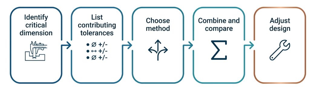
- Determine the critical dimension that could fail.
- Select your approach: Worst-Case for safety margin or RSS / Monte Carlo for realism.
- Add the tolerances together and compare to your lowest requirement.
- If the margin is too thin, try changing pad sizes, pad clearances, or layers.
- Lower manufacturing defects and higher yields.
Benefits of Thorough Tolerance Analysis
Reduced Manufacturing Defects and Higher Yield Rates
The primary benefit today is yield. The more that you size your features to accommodate realistic variation, the fewer boards that fall out of any acceptable bounds during fabrication and assembly. That directly increases your rate of yield. Defects such as annular ring breakout, solder bridging, and impedance drift are typically tolerance issues in disguise. These are caught on the screen, rather than the inspection bench, when analyzing the stack prior to release. IPC standards like IPC-A-600 tell what is acceptable, and tolerance analysis is the way to remain in those classes comfortably. The higher the yield, the more predictable the lead times. Boards that don't require rework move smoothly up the line, and this is important if you're going from prototype to production.
Lower Costs Through Fewer Revisions and Scrap
Each board failure is wasted material, energy, and time. There's the obvious cost if a design change takes you back through layout, fabrication, and validation. Those are not simply dollars; those are weeks! Tolerance analysis “front-loads” the effort into the design stage, where it is less expensive to make changes. It takes minutes to catch a thin annular ring in CAD, and a fortune to catch it after a 1,000 board run. A few hours of analysis can produce a huge return. There is also an argument about a sweet spot here. If all tolerances are tightened up, the fabrication cost is increased, and if they are loosened up, the non-critical tolerances, the money is saved. Correct analysis will help you know which functions require accuracy and which can be unwound.
JLCPCB's Professional Approach to Tolerance Analysis
Advanced DFM Review with Detailed Tolerance Feedback
This is where a good manufacturing partner is useful. Before boards are even manufactured, JLCPCB performs an automatic Design for Manufacturability (DFM) check on all orders to highlight features that exceed its own published tolerance and capability limits. That feedback is real-world. If the annular ring is marginal, the drill-to-copper spacing is small, or the trace width is smaller than the minimum that can be etched reliably, the system increases the width of the ring to allow easy correction at minimal cost in CAD. This does a first pass tolerance check for you.

Starting from $2 and turnaround as quick as 1-2 days, the ability to prototype and test tolerance assumptions against real boards while scaling up with confidence. The key to reliable, cost-effective production is that feedback loop - design, measure, refine.
Precision Process Control Across All Fabrication Stages
The analysis without a process to get those numbers is only as good as the process. JLCPCB has strict control over drilling, etching, lamination, and plating processes to ensure that the actual boards are within the limits specified in their DFM. That control encompasses the areas we discussed above:
- The accuracy of the hole diameter and the uniformity of the plated finishes
- Control of etch for predictable trace and space width
- Reliable multilayer stacks using layer-to-layer registration.
- Registration of solder mask for fine pitch solder openings.
FAQ abouot Tolerance Analysis
Q: What is PCB tolerance analysis in simple terms?
It is the process of calculating how small manufacturing variations in holes, traces, and layers combine to affect the finished board. The goal is to confirm that even in the worst realistic case, your design still assembles and works correctly.
Q: What is the difference between Worst-Case and RSS analysis?
Worst-Case adds every tolerance at its extreme in the same direction, which is the most conservative result. RSS uses a root-sum-square statistical combination assuming normal distributions, giving a more realistic stack because all features rarely hit their limits at once.
Q: What are typical PCB fabrication tolerances I should plan for?
Common values include hole diameter around +/-0.05 mm to +/-0.1 mm, plus etch tolerance on trace and space, layer-to-layer registration error, copper weight variation, and solder mask registration. Always check your specific fabricator's published capability sheet for exact numbers.
Q: When should I use Monte Carlo instead of RSS?
Use Monte Carlo when your dimensional stack is complex, or the variations do not follow a normal distribution. It randomly samples each dimension thousands of times to map the true spread of outcomes, giving the most realistic prediction when you have good process data.
Q: How does tolerance analysis reduce manufacturing cost?
It catches marginal features in the design phase, where fixes are cheap, instead of after a production run. This reduces scrap and costly respins, while also showing which tolerances truly need to be tight so you do not overpay for unnecessary precision.
Conclusion
One of those lesser-known disciplines is tolerance analysis, which is what differentiates a design that looks like it's ready to roll from a design that ships reliably. Knowing that every hole, trace, and layer has real-world variation and using the real-world variation coupled with Worst-Case, RSS, or Monte Carlo methods, you trade hope for proof. The increased payout is reflected in a higher return, fewer re-spins, and lower scrap. The tighter margins and the greater density and speed of boards are only going to increase the importance of tolerance stack-up analysis. To implement these principles, JLCPCB's automated DFM review and precise fabrication ensure that tolerances meet the actual production requirements. Plan for the variation, test for variations, and your products will thank you.
Keep Learning
Why Tolerance Analysis Is Key to Reliable and Cost-Effective PCB Production
Key Takeaways Tolerance analysis bridges CAD perfection and manufacturing variations to ensure reliable PCB assembly. Focus on critical areas: annular rings, hole tolerances, trace/space, layer registration, and solder mask alignment. Apply Worst-Case, RSS, or Monte Carlo methods for effective tolerance stack-up. Proper analysis boosts yield, cuts respins and costs — start with JLCPCB’s DFM review. Have you ever sent a board to fabrication, which appeared flawless on the computer screen, but then foun......
The Ultimate Guide to PCB Panelization: Tools and Techniques
Printed circuit boards (PCBs) are the backbone of modern electronics. One critical aspect of PCB manufacturing is panelization — the process of arranging multiple PCBs onto a single larger panel for efficient manufacturing and assembly. This technique allows multiple boards to be processed simultaneously, significantly reducing costs and improving production efficiency. In this article, we will provide a comprehensive guide to PCB panelization, covering the tools and techniques required for successful......
Castellated PCBs: Introduction and Design Requirements
With the rapid development of electronic technology, electronic products are moving towards miniaturization, portability, multi-functionality, high integration, and high reliability.Consequently, printed circuit boards (PCBs) are frequently designed to integrate pre-existing, off-the-shelf modules. For example, IoT Bluetooth modules or NB-IoT modules, which are indispensable communication modules, can be soldered onto PCBs just like chips. These carrier boards are characterized by their small size and......
Copper Balancing in PCBs: Achieving Optimal Performance and High Yields with JLCPCB
Key Takeaways Copper balancing strategically distributes copper across PCB layers to create uniform density, preventing warpage, uneven plating, inconsistent etching, and signal integrity issues. The ideal copper density target sits within the 40%–60% golden ratio, with mirrored layers maintaining density variation within 15%–20% per IPC-6012 standards. Copper thieving (dot patterns or crosshatch meshes) equalizes current density during electroplating without introducing parasitic capacitance on spars......
PCB Design : How to Resolve Short Circuit Defects Caused by HASL
Key Takeaways In high-density PCB designs, HASL frequently causes solder bridging and short circuits due to its uneven surface and molten solder flow, especially on fine-pitch and dense traces. The most effective solution is to switch to ENIG (Electroless Nickel Immersion Gold), which provides superior planarity, significantly reduces bridging risks, and improves assembly yield. By selecting ENIG for dense layouts, optimizing solder mask design, and running DFM checks, designers can effectively elimin......
Design Process of a Surface Mount PCB
Key Takeaways Mastering the surface mount PCB design process is essential for creating compact, high-density, and reliable electronic boards. This comprehensive guide walks through the complete SMT workflow — from schematic capture and component selection to optimized layout, precise routing, DRC/ERC verification, and Gerber file generation — enabling designers to achieve superior performance, better manufacturability, and cost efficiency compared to traditional through-hole methods. By following thes......