
What Is Solder Paste? A Complete Guide to Composition, Uses, and PCB Assembly
18 min
- What Is Solder Paste?
- What Is Solder Paste Used For?
- What Is Solder Paste Made Of?
- How Solder Paste Works in PCB Assembly
- Types of Solder Paste
- How to Choose the Right Solder Paste for Electronics
- How Solder Paste Is Applied to PCBs
- How to Use Solder Paste using Stencil: Step by Step
- Best Practices for Using Solder Paste
- Common Solder Paste Defects in PCB Assembly
- Solder Paste vs Flux: What’s the Difference?
- Solder Paste vs. Solder Wire: Which One to Use?
- JLCPCB High-Precision Solder Paste Printing in PCB SMT Assembly
- FAQ About Solder Paste
- Conclusion
Solder paste is a thick, gray putty made by mixing microscopic metal solder powder with a sticky flux binder. In electronics manufacturing, it is primarily used in Surface Mount Technology (SMT) to temporarily glue surface-mount components to a printed circuit board (PCB). Once heated in a reflow oven, the paste melts to form permanent, highly reliable electrical and mechanical connections.
In this comprehensive guide, we will explore:
- Solder Paste Composition: The exact blend of solder alloy powder and flux binder.
- Core Functions: Its essential role in SMT and electronics manufacturing.
- Different Types Available: How to navigate alloys, flux systems, and IPC particle sizes.
- Application Methods: Step-by-step guidance on how to apply it perfectly in your next PCB assembly project.
What Is Solder Paste?
The development of solder paste triggered a major transformation in electronics manufacturing. By leveraging complex suspension physics, it maintains a stable rheological balance between dense, microscopic metal powder and a lighter, thixotropic chemical flux.
This material represents the crucial technological leap that made modern Surface Mount Technology (SMT) possible, allowing the industry to move away from bulky, space-consuming through-hole soldering. Because it acts as a printable, temporary adhesive that later transforms into a permanent, highly conductive metallurgical bond, it serves as the primary driver behind the miniaturization of modern devices. Without this rheological balance, the mass production of dense, complex PCBA (Printed Circuit Board Assembly) would be entirely impossible.
Why Solder Paste Is Essential in Electronics Manufacturing
As electronic devices shrink, components like microprocessors and passive resistors become too small for human hands to solder individually with a traditional iron. Solder paste allows manufacturers to print conductive material precisely onto thousands of microscopic pads simultaneously, enabling high-speed, high-density manufacturing.
Role of Solder Paste in SMT Assembly
During SMT assembly, solder paste plays a dual role. First, its tacky nature (referred to as "tackiness") holds surface-mount components precisely where they are placed. Second, when heated to its melting point, it forms a permanent metallurgical bond between the component lead and the PCB pad.
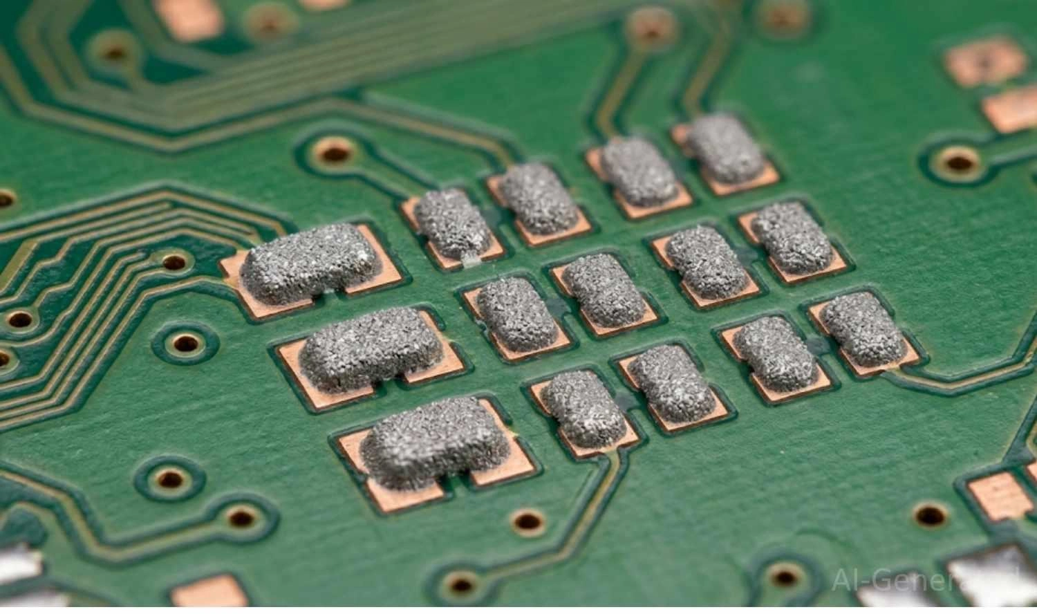
Figure: Macro view of freshly printed solder paste bricks resting perfectly on a bare green printed circuit board's copper pads.
What Is Solder Paste Used For?
Understanding what solder paste is used for comes down to three primary functions in circuit board fabrication:
Creating Reliable Electrical Connections
The primary job of solder paste for electronics is to create a seamless, low-resistance electrical pathway. Once melted, the alloy flows and adheres to both the SMD components and the copper pads on the PCB, ensuring flawless signal and power transmission.
Mechanical Fixation of SMD Components
Circuit boards endure drops, vibrations, and thermal cycling. A properly formed solder joint provides the mechanical strength needed to keep heavy components fixed firmly to the board without snapping off.
Enabling Automated PCB Mass Production
Solder paste allows the industry to move away from slow manual soldering. Through automated SMT assembly, paste is quickly squeegeed over a stencil, components are rapidly placed by machines, and entire panels are soldered in minutes inside an oven.
What Is Solder Paste Made Of?
To understand how solder paste works, we must look at its two primary ingredients: solder alloy powder and flux medium.
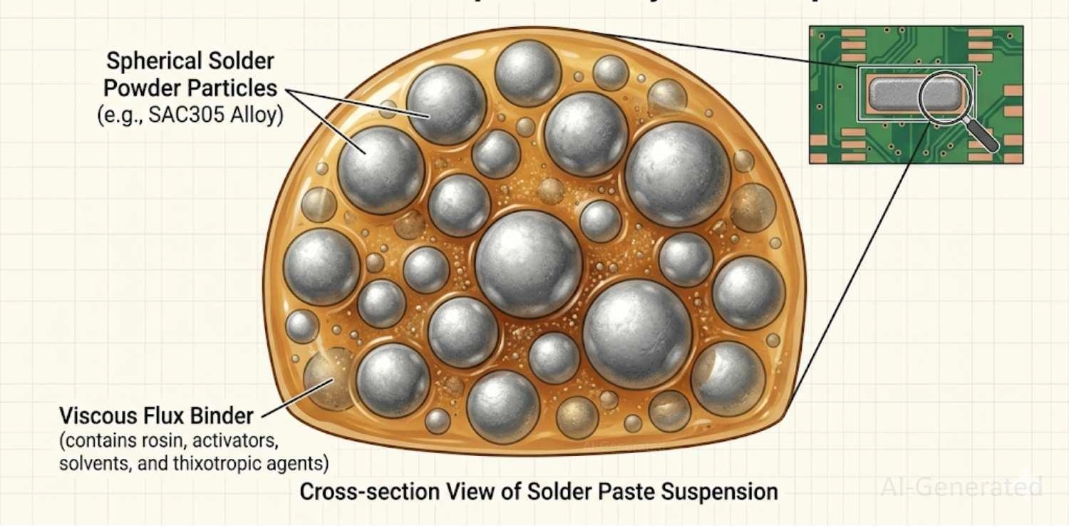
Figure: Microscopic anatomy and composition of solder paste showing round metal solder powder spheres suspended in a viscous chemical flux binder.
Solder Alloy Powder (Tin, Silver, Copper)
The metal portion makes up roughly 85% to 90% of the paste by weight (but only about 50% by volume). Historically, this was a blend of Tin and Lead (SnPb). Today, strict environmental regulations mandate lead-free solder paste, most commonly the SAC305 alloy (96.5% Tin, 3.0% Silver, 0.5% Copper).
Flux Binder and Its Function
Flux is a chemical cleaning agent. During the heating process, flux activates and dissolves the microscopic oxidation layers on both the PCB pads and the component leads. Without flux, the molten metal would just roll off the pads rather than bond to them. It also acts as an oxygen barrier to prevent re-oxidation during the high-temperature reflow stage.
Additives That Improve Performance
Advanced pastes include thixotropic agents and specialized solvents. These chemicals give the paste special rheological properties: it becomes thinner and flows easily when pushed through a stencil by a squeegee, but instantly thickens up once printed, preventing it from slumping and causing short circuits.
Alloy Type | Common Composition | Melting Point | Best For |
|---|---|---|---|
Leaded | Sn63/Pb37 | 183°C | Hobbyists, legacy aerospace, repairs |
Lead-Free (SAC305) | Sn96.5/Ag3.0/Cu0.5 | 217°C - 220°C | Modern consumer electronics (RoHS) |
Low-Temp | Sn42/Bi57/Ag1 | 138°C | Heat-sensitive components, flex PCBs |
How Solder Paste Works in PCB Assembly
Solder Paste Printing/Deposition
The process begins by aligning a laser-cut stainless steel stencil over the bare PCB. A blade (squeegee) pushes the solder paste across the stencil, depositing precise blocks of paste onto the exposed copper pads.
Component Placement
Next, a robotic Pick-and-Place machine shoots tiny components onto the paste blocks. The tacky flux acts like glue, keeping the components from shifting as the board moves down the conveyor belt.
Reflow Soldering Process
The populated board enters a large oven for reflow soldering. The oven runs a specific thermal profile consisting of four stages:
- Preheat: Gradually ramps up the temperature to prevent thermal shock in components.
- Soak: Flux activates to clean the pads and evaporate solvents.
- Reflow: The temperature spikes past the melting point, turning the powder into liquid metal.
- Cooling: The metal rapidly solidifies into strong, shiny solder joints.
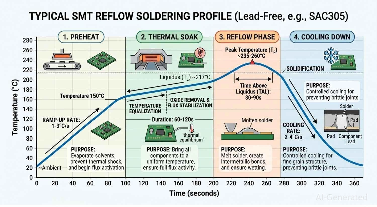
Figure: Temperature versus Time graph detailing the four stages of an SMT reflow soldering profile: preheat, thermal soak, reflow phase, and cooling down.
Types of Solder Paste
When ordering supplies or using a manufacturing service, you will notice many types of solder paste. They are generally classified in three ways:
Classification by Alloy Composition
- Lead-based solder paste: Highly reliable and easy to melt (183°C), but toxic. Banned in consumer electronics but still used in specific military/aerospace niches.
- Lead-free solder paste: The modern industry standard (like SAC305). Requires higher temperatures to melt and careful thermal management.
Classification by Flux System
- No-clean solder paste: Leaves a benign, non-corrosive residue after reflow that doesn't need to be washed off. This is the most common type used today.
- Rosin-based solder paste (RMA): Contains mildly activated rosin. Highly effective but leaves a sticky residue.
- Water-soluble solder paste: Contains aggressive organic fluxes that produce perfect joints, but the corrosive residue must be washed off immediately with deionized water.
Classification by Particle Size (IPC Types)
Solder powder is graded by the physical size of its metallic spheres.
- Type 3: The standard for general SMT work (25-45 microns). It is the most common and cost-effective choice, ideal for components with a pitch of 0.5mm or larger and passive packages down to 0402.
- Type 4: Smaller spheres (20-38 microns), great for tighter component spacing. It is increasingly the go-to for high-density boards featuring 0201 passives or ICs with a 0.4mm pitch.
- Type 5: Very fine spheres (15-25 microns), typically reserved for components with a pitch of 0.35mm or smaller, making it mandatory for ultra-tight components like fine-pitch BGA packages.
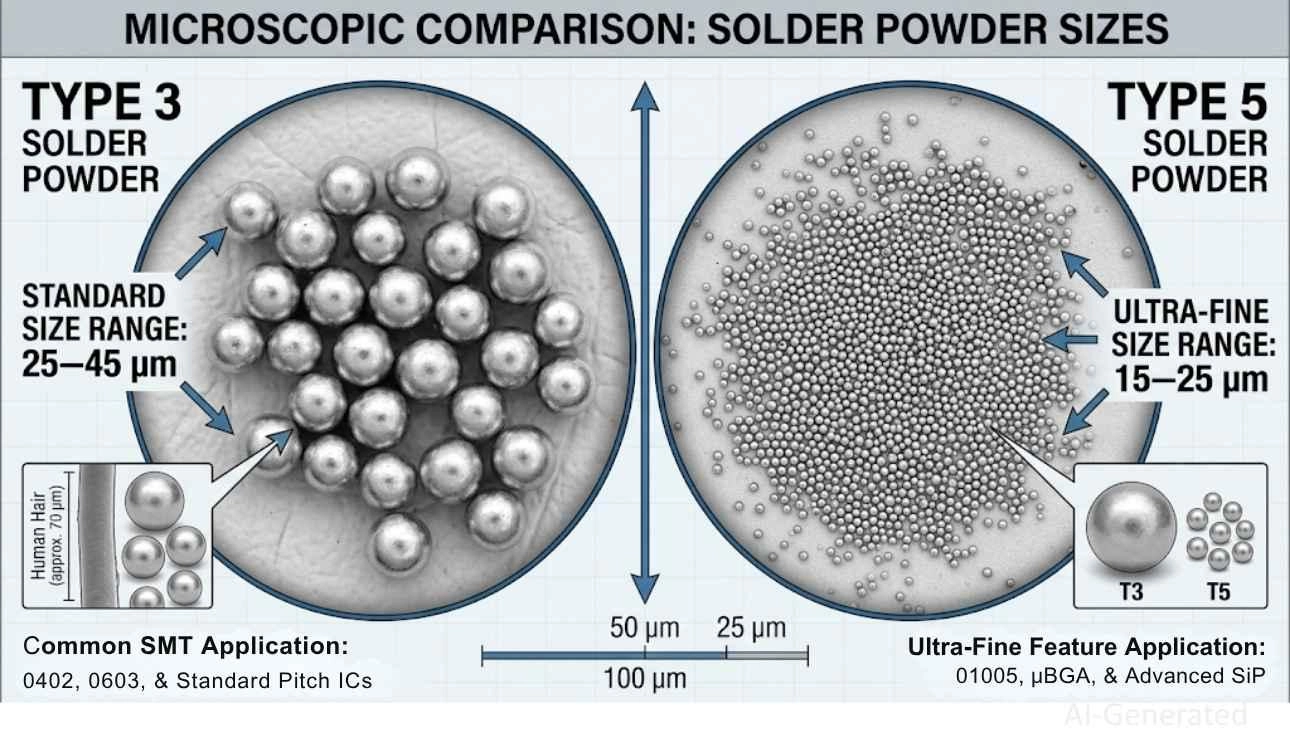
Figure: The visible size difference between standard Type 3 solder spheres and ultra-fine Type 5 solder spheres.
Specialized Solder Paste Types
For delicate LEDs or flex boards, engineers use Low-temperature solder paste (often Bismuth-based). In extreme environments such as automotive engines, High-reliability pastes with specialized alloys are used.
Type | Particle Size / Specs | Application | Pros | Cons |
|---|---|---|---|---|
Type 3 (Standard) | 25-45 microns | General SMT, 0402 components | Cost-effective, less prone to oxidation | Too large for fine-pitch parts |
Type 4 (Fine) | 20-38 microns | High-density SMT, 0201 parts | Good balance of printability & size | Shorter shelf life, higher cost |
Type 5 (Ultra-Fine) | 15-25 microns | Micro-BGA, ultra-fine pitch | Excellent for micro-components | Very sensitive to humidity/oxidation |
No-Clean Flux | N/A | Consumer electronics, fast prototyping | Leaves a benign residue, saves cleaning | Residue can interfere with high-frequency RF |
Water-Soluble Flux | N/A | High-reliability, aerospace, medical | Creates perfect joints, highly active | Requires immediate, thorough washing |
How to Choose the Right Solder Paste for Electronics
Choosing Solder Paste by Application Type
Match the alloy to your project. If you are building consumer electronics intended for sale, you must use lead-free (RoHS-compliant) paste. If you are repairing vintage electronics, standard 63/37 leaded paste is safer for the older board materials.
Selecting the Right Flux System
For 90% of makers and engineers, No-clean flux is the best choice because it eliminates the tedious board-washing step. Water-soluble is generally reserved for advanced manufacturing facilities with inline wash systems.
Matching Particle Size to Components
If your board features macroscopic parts, Type 3 is highly cost-effective. However, if your design features ultra-compact 0201 resistors or dense microcontrollers, you must step up to a Type 4 or Type 5 paste so that the tiny stencil apertures don't clog.
Recommended Solder Paste for Beginners
If you are learning how to use solder paste, start with a syringe of Type 3 or Type 4 No-clean paste (leaded Sn63Pb37 is easiest to melt, but SAC305 is safer). Syringes allow for easy manual dispensing without needing a stencil.
How Solder Paste Is Applied to PCBs
Stencil Printing Method (Most Common)
For PCB prototypes and mass production, a laser-cut stainless-steel framed stencil is aligned precisely over the board. A squeegee (typically made of metal or rigid polyurethane) held at a 45-to-60-degree angle applies uniform pressure to shear the paste through the cutouts onto the pads. The separation speed—how fast the stencil lifts away from the board - is also tightly controlled to ensure the paste "bricks" release cleanly without dog-ears or slumping.
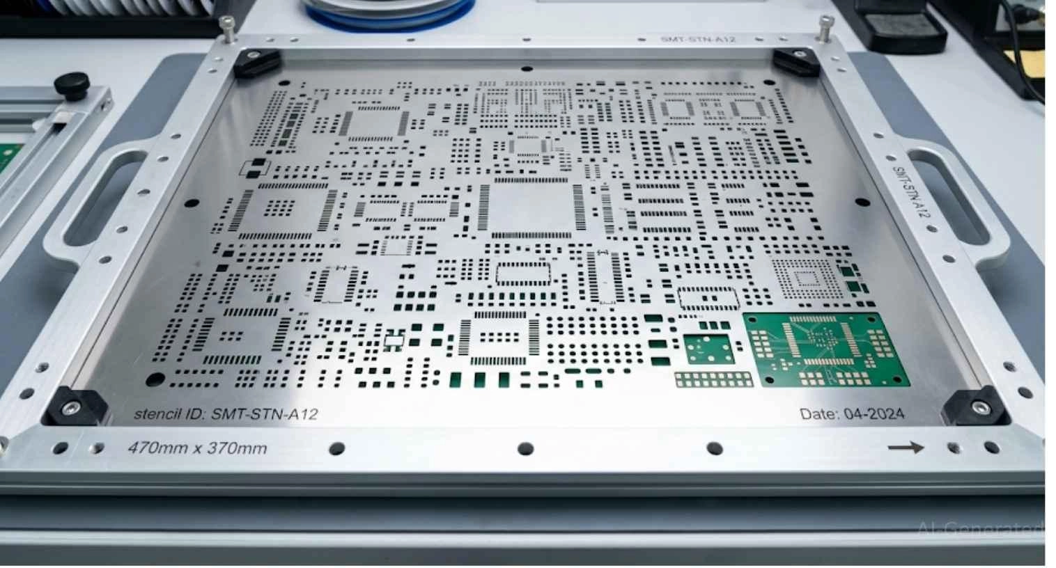
Figure: A laser-cut stainless steel SMT stencil mounted in an aluminum frame, showing the precise cutouts used to define solder paste deposition on a bare PCB.
Manual Application for Prototyping and Repair
If you are building a single prototype or replacing a broken IC, you can use a pneumatic dispenser or a manual plunger syringe. Using a fine-gauge dispensing needle, you simply squeeze a tiny, controlled dot of paste onto each pad. While accessible and easy to set up, manual dispensing requires a steady hand and can result in inconsistent paste volumes, making it unsuitable for highly complex, fine-pitch components.
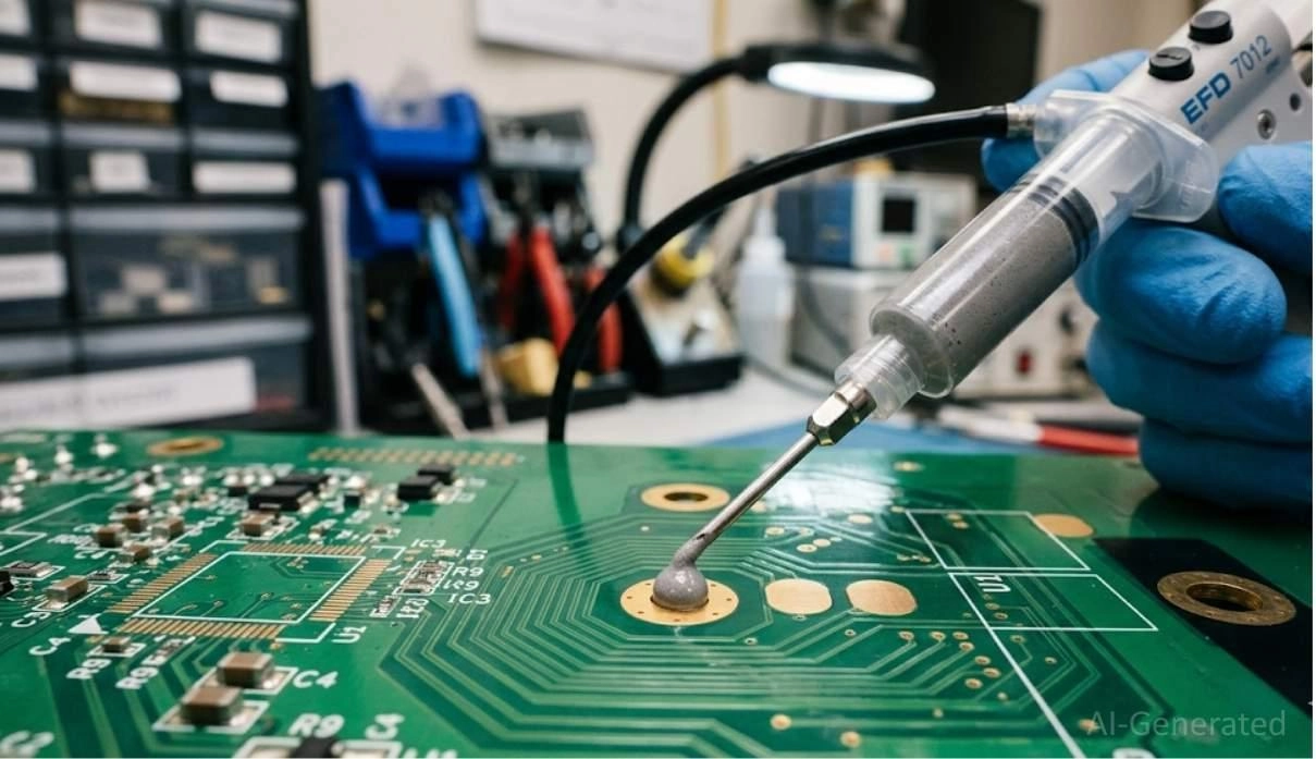
Figure: Close-up of a manual pneumatic syringe dispensing a precise dot of gray solder paste onto a single copper PCB pad.
Automated SMT Production
In advanced manufacturing lines, fully automated screen printers use high-definition fiducial cameras to align the stencils with microscopic precision.
These machines are often paired with inline 3D Solder Paste Inspection (SPI) systems to instantly scan and verify the exact volume, height, and shape of every printed pad before components are placed. For highly complex or stepped boards, some bleeding-edge factories use Jet Printing.
This technology shoots tiny droplets of paste onto the board much like an inkjet printer, completely bypassing the need for stencils and allowing for on-the-fly volume adjustments for individual pads.
How to Use Solder Paste using Stencil: Step by Step
Step 1 - Bring Solder Paste to Room Temperature
Before applying solder paste, it must be properly thawed from refrigeration. Allow the sealed container to sit at room temperature for 2 to 4 hours. Never open cold solder paste; opening it while cold allows condensation to form, which introduces moisture and severely degrades the flux. Once warmed to room temperature, gently stir it for 1 to 2 minutes to restore its smooth, flowing rheological consistency.
Step 2 - Prepare and Clean the PCB Pads
The bare circuit board must be completely free of contaminants. Use 99% isopropyl alcohol (IPA) and a lint-free wipe to remove any dust, microscopic oils from fingerprints, and oxidation. Clean pads are essential to ensure the flux can activate properly and promote excellent solder wetting across the copper surface.
Step 3 - Align the Stencil Over the PCB
Carefully position and fix the laser-cut stainless steel stencil over the circuit board. Perfect aperture alignment is critical. Even a fraction of a millimeter of misalignment can result in paste being deposited off the copper pads, which will cause solder bridges, tombstoning, or weak joints later in the process.
Step 4 - Print / Dispense Solder Paste on Pads
Using a metal squeegee held at a 45-to-60-degree angle, push the paste across the stencil in one smooth, continuous pass. Apply consistent pressure to ensure uniform paste deposition across all pads while avoiding excessive pressure that might scoop paste out of the apertures. For manual dispensing with a syringe, apply precise dots to the center of each pad, being careful to avoid excess paste.
Step 5 - Inspect the Printed Solder Paste Deposits
Once printed, carefully lift the stencil away from the board vertically and immediately inspect the printed deposits. Look for uniform paste height, sharp edges indicating excellent stencil release quality, and a flat top. Ensure there is no smearing between adjacent pads, as smeared paste carries a very high bridging risk during the reflow stage.
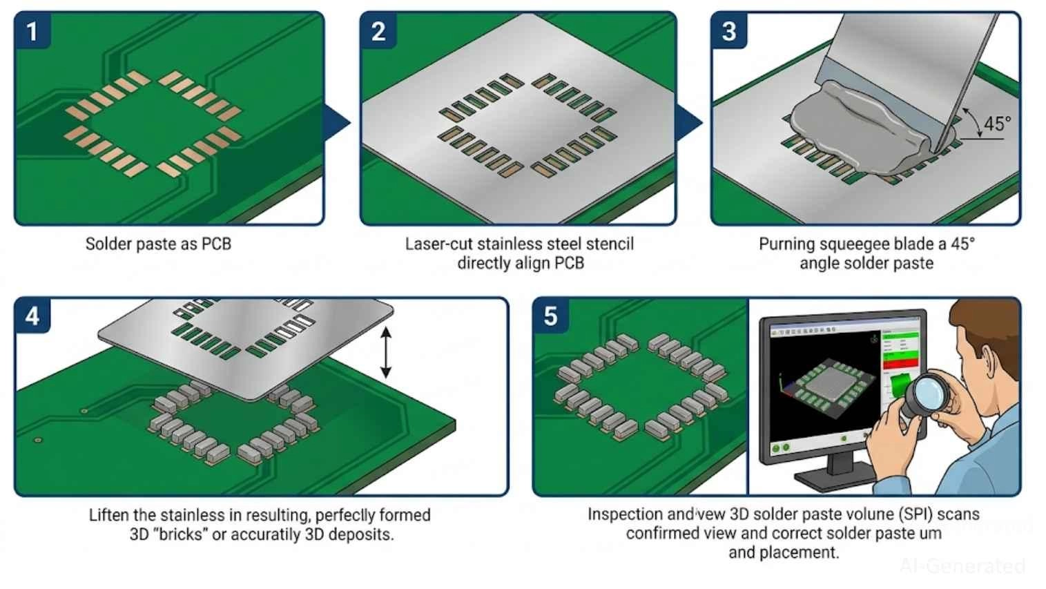
Figure: Five-step process for solder paste deposits
Best Practices for Using Solder Paste
- Proper Storage and Handling: Solder paste has a strict shelf life (usually 3 to 6 months) and must be refrigerated (2°C - 10°C) to prevent the flux from degrading. Never open cold solder paste! Let it sit at room temperature for 2-4 hours before opening to prevent water condensation from ruining the paste. Gently stir it in a jar for 1–2 minutes before use to restore its smooth, flowing rheology.
- Monitor Tack Life After Printing: In addition to shelf life, solder paste has a strict "tack life" once exposed to the air. It is highly recommended to complete component placement and reflow within 2 to 4 hours after printing. Otherwise, the solder paste will dry out, leading to component misalignment or poor wetting during the reflow stage.
- Correct Stencil Design: Achieving the perfect print relies heavily on stencil quality. Ensure the stencil thickness and aperture area ratio are correctly matched to your components. An optimized design guarantees the paste releases cleanly from the stencil walls without clogging.
- Temperature and Humidity Control During Reflow: Solder paste is highly sensitive to environmental conditions. Keep the manufacturing floor between 20°C and 25°C with a relative humidity of 40%-50%. High humidity causes the paste to absorb moisture (resulting in solder balling), while dry conditions cause it to dry out, losing its tackiness before it even reaches the reflow oven.
Common Solder Paste Defects in PCB Assembly
- Solder Bridges: Occurs when too much paste is applied, causing two adjacent pins to short-circuit together.
- Tombstoning: When paste is applied to one side of a tiny resistor, it melts faster than the other side; surface tension pulls the component upright, resembling a tombstone.
- Insufficient Solder: Caused by clogged stencils, resulting in weak or open electrical connections.
- Solder Balling: Tiny, isolated spheres of solder that scatter across the board, often caused by excessive moisture in the paste or too rapid preheating.
- Head-in-Pillow (HiP): A dreaded defect, especially in BGA packages, where the paste melts but fails to coalesce with the component sphere, leaving a hidden, weak connection that resembles a head resting on a pillow.
- Voiding: Air or flux gas trapped inside the solder joint. While small voids are acceptable, large voids can severely compromise the joint's mechanical strength and thermal conductivity.
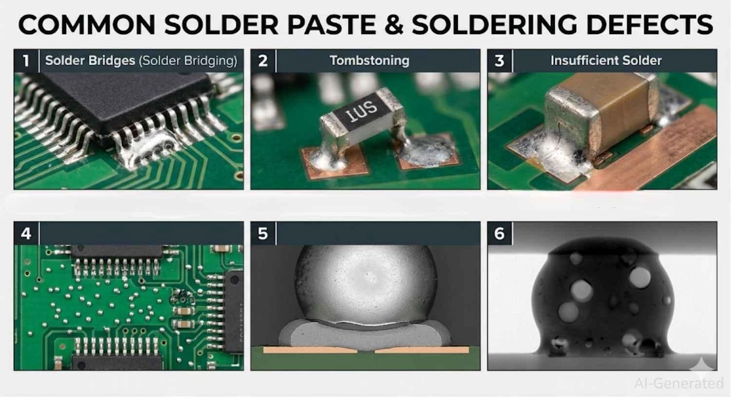
Figure: Visual examples of solder paste-related defects
Solder Paste vs Flux: What’s the Difference?
Is solder paste the same as flux? No. While beginners sometimes interchange the terminology, they serve entirely different purposes in the PCB assembly process.
Composition Differences
Flux is purely a chemical cleaning agent (usually a liquid or gel) made from rosins, resins, or organic acids. Solder paste is a carefully balanced mixture consisting of that exact chemical flux plus microscopic, solid metal alloy powder.
Application Differences
Flux is brushed, sprayed, or dispensed directly over bare copper or existing joints strictly to remove oxidation and aid in heat transfer. Solder paste is printed onto pads through a stencil specifically to deposit new metal where there previously was none.
When to Use Solder Paste
You should use solder paste when assembling a bare circuit board from scratch using SMT components, or when you are using a hot air rework station to attach a brand new microchip that requires fresh metal on its pads.
When to Use (Standalone) Flux
You should use standalone flux when re-melting an existing joint to fix a defect (like clearing a solder bridge), when using standard solid wire with a soldering iron, or when cleaning up old pads with copper desoldering wick.
Solder Paste vs. Solder Wire: Which One to Use?
While both materials achieve the same end goal-forming a permanent metallurgical bond-their manufacturing use cases and application methods are entirely distinct.
Application Differences (SMT vs Manual Soldering)
Solder paste is strictly designed for Surface Mount Technology (SMT). It is intended to be printed onto flat pads and melted collectively inside a reflow oven. Solder wire (usually containing a rosin core) is designed for Through-Hole Technology (THT), wire splicing, and manual hand-soldering with a traditional heated iron.
Joint Quality and Process Control
Because solder paste is pushed through precision laser-cut stencils, it deposits the same volume of metal onto every single pad, ensuring 100% consistency across thousands of joints. Conversely, solder wire relies entirely on the human operator's manual skill to feed the correct amount of metal, making perfectly uniform joints much harder to achieve.
Production Efficiency Considerations
Solder paste allows automated lines to place thousands of components and solder them simultaneously in a matter of minutes, driving mass production. Wire soldering is a sequential, pin-by-pin process that is incredibly slow, making it suitable only for very low-volume work, PCB prototyping, or post-reflow component additions (like attaching bulky through-hole connectors).
JLCPCB High-Precision Solder Paste Printing in PCB SMT Assembly
Applying solder paste perfectly is arguably the most critical step in electronics manufacturing - over 70% of all PCBA defects originate from poor paste printing. For engineers seeking flawless, commercial-grade electronics, leveraging a professional assembly service is highly recommended.
JLCPCB utilizes industry-leading, fully automated 3D solder paste inspection (SPI) machines and ultra-precise stencils to guarantee flawless paste deposition. To further guarantee process stability, JLCPCB operates under strict environmental control, maintaining optimized temperature and humidity levels within its SMT cleanrooms. This controlled environment is critical for preserving solder paste rheology, preventing premature drying, and ensuring consistent print quality across both prototype and mass production runs.
Whether you are scaling a low-volume PCBA or moving to mass production, JLCPCB ensures your components are securely and reliably soldered.
You can easily select your required electronic parts from their extensive library and get a rapid online quotation to bring your design to life.

FAQ About Solder Paste
Q: Can solder paste be used with a soldering iron?
Yes, but it is not ideal. While a soldering iron will melt the paste, the liquid flux tends to spatter rapidly, and it is much harder to control the amount of solder compared to using standard rosin-core solder wire. Solder paste is primarily designed for hot air stations or reflow ovens.
Q: Can solder paste go bad?
Yes. Solder paste has a strict shelf life, usually between 3 and 6 months when properly refrigerated. Once it goes bad, the flux degrades, the metal powder oxidizes, and the paste loses its tackiness, leading to severe soldering defects.
Q: How long does it take to reflow solder paste?
A typical reflow soldering profile takes about 3 to 6 minutes from start to finish. This includes slowly preheating the board, soaking it to activate the flux, briefly spiking the temperature (usually for 30-90 seconds) to melt the alloy, and finally cooling it down.
Q: How to tell if solder paste has expired?
If the paste separates (flux pooling at the top) and refuses to mix back into a smooth, buttery consistency, or if components won't stick to it during placement, it has expired and should be safely discarded.
Conclusion
Solder paste is a remarkable engineering material that bridges the gap between raw circuit boards and fully functioning electronic devices. By understanding what solder paste is, its chemical composition, and the nuanced differences between particle sizes and flux types, you can eliminate manufacturing defects and build highly reliable hardware.
Whether you are printing paste manually for a weekend project or utilizing JLCPCB’s automated SMT lines, mastering this step is the ultimate key to achieving a perfect soldering result.
Popular Articles
• How to Identify SMD LED Polarity: Markings, Testing, and PCB Tips
• How to Create a Bluetooth-Controlled Car With Arduino: A Step-by-Step Guide
• How to Design and Assemble a Reliable ESP32 Module PCB on a 2-Layer Board
• The Ultimate Guide to Relay Symbol: Coil, Contacts, Diagrams, and Circuit Applications
• The Ultimate Guide to PCBA: Process,Types and Techniques for the Electronics Enthusiast
Keep Learning
How to Design an ESP32-S3 Development Board from Scratch: A 4-Layer PCB Design Tutorial
Designing your own ESP32-S3 development board gives you complete control over your hardware architecture while preparing your IoT projects for commercial production. Instead of relying on bulkier, off-the-shelf boards, building a custom design allows you to optimize the board space, expose only the required GPIO pins, and integrate peripherals directly onto a single substrate. In this tutorial, we will design a 4-layer ESP32-S3 development board from scratch. We will walk through the entire hardware d......
Circuit Breaker Symbols Explained: IEC, ANSI, MCB, and Pole Configuration Symbols
Electrical schematics are the universal language of power systems, control circuits, and printed circuit boards. Within these diagrams, the circuit breaker symbol is one of the most critical elements. Getting it right is essential for safety, troubleshooting, and manufacturing. An error as simple as mixing up a circuit breaker with a manual switch or an isolator can lead to catastrophic misinterpretations on the factory floor or during field maintenance. This guide provides a complete, technically acc......
How to Identify SMD LED Polarity: Markings, Testing, and PCB Tips
Surface-mount LED components are ubiquitous in electronics design, serving as everything from simple power indicators to complex lighting arrays. Unlike standard resistors, LEDs are polarized diodes. Identifying SMD LED polarity correctly is critical for prototype troubleshooting and high-volume PCB assembly. A reversed LED results in no light output, broken circuit paths, and potential diode breakdown if the reverse voltage exceeds the component's maximum rating (typically 5V or less for most indicat......
Arduino LED Driver Tutorial: Control More LEDs with 74HC595 and MAX7219
Arduino GPIO pins run out quickly in larger LED projects. By utilizing dedicated LED drivers and expansion ICs, you can drastically reduce pin usage, eliminate processor-heavy multiplexing loops, and simplify display wiring. In this guide, you will learn the operational architecture, wiring configurations, cascading techniques, and optimization strategies for the 74HC595 shift register and the MAX7219 LED driver. Why Arduino Projects Need LED Driver ICs Arduino GPIO and Current Limitations An ATmega32......
How to Create a Bluetooth-Controlled Car With Arduino: A Step-by-Step Guide
This tutorial walks through the complete engineering and implementation of a two-wheel Bluetooth RC car with an Arduino Nano module on a specially designed PCBA (Printed Circuit Board Assembly). While many hobbyists start by wiring motors and Bluetooth modules with jumper cables on a breadboard, this approach is prone to disconnection and signal noise. This guide upgrades that process by teaching you how to design a professional mainboard. Key Design Features Controller: Arduino Nano used as a plug-in......
Fiducial Marks in PCB and SMT Assembly: A Complete Guide to Accuracy and Design Rules
Modern Printed Circuit Boards (PCBs) are complex, integrating high-density components like 0.4mm pitch Ball Grid Arrays (BGAs), 0201 passives, and fine-pitch Quad Flat No-Lead (QFN) packages. In this advanced manufacturing environment, achieving placement accuracy measured in micrometers is crucial. A significant challenge in automated manufacturing is how pick-and-place machines, which handle thousands of components per hour, precisely locate the PCB. A board on a conveyor system is never in the perf......