
The Ultimate Guide to IC Symbol: Meaning, Types & Circuit Diagram Examples
10 min
- What is the Symbol of an Integrated Circuit?
- How Integrated Circuit Symbols Work (Pins & Functional Blocks Explained)
- Types of Integrated Circuit Symbols
- How to Read an Integrated Circuit Symbol
- Common Mistakes When Reading IC Symbols
- Integrated Circuit Package vs. Schematic Symbols (DIP, SMD & Pin Mapping)
- Common Integrated Circuit Symbol Examples in Real Circuits
- Integrated Circuit Symbol vs Other Electronic Symbols
- From Integrated Circuit Symbol to PCB Design and Assembly
- FAQs About Integrated Circuit Symbol
- Conclusion
Think of an integrated circuit (IC) as a microscopic city of electronics. Instead of drawing hundreds of individual components, engineers use an integrated circuit symbol to represent the entire system as one clean block.
While the physical chip might look like a tiny black bug with metal legs, the IC schematic symbol explained on paper is a functional map. Understanding these electronic IC symbols makes designing and troubleshooting infinitely easier.
What you will learn in this guide:
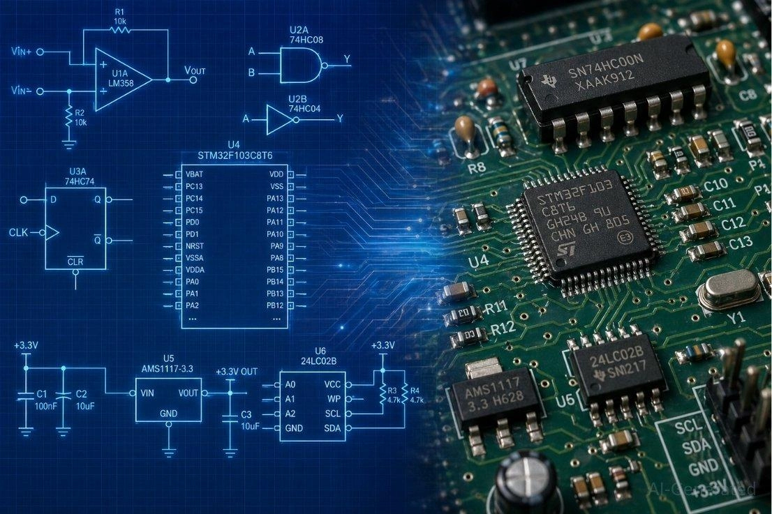
Figure: Illustration of the transition from various integrated circuit schematic symbols to real physical IC components mounted on a PCB.
What is the Symbol of an Integrated Circuit?
The standard integrated circuit symbol is a rectangular block representation. It intentionally hides the complexity of multiple internal components, providing a clean interface of inputs and outputs for the engineer to work with.
Why Integrated Circuit Symbol Used in Circuit Diagrams
- Simplifies complex circuits: Prevents schematic diagrams from becoming unreadable spiderwebs.
- Represents multiple components as one: Consolidates thousands of microscopic parts into a single logical block.
Where Integrated Circuit Symbols Are Used
You will find these symbols in nearly every modern schematic, from analog devices to digital embedded systems. They represent amplifiers, programmable microcontrollers, and essential logic circuits.
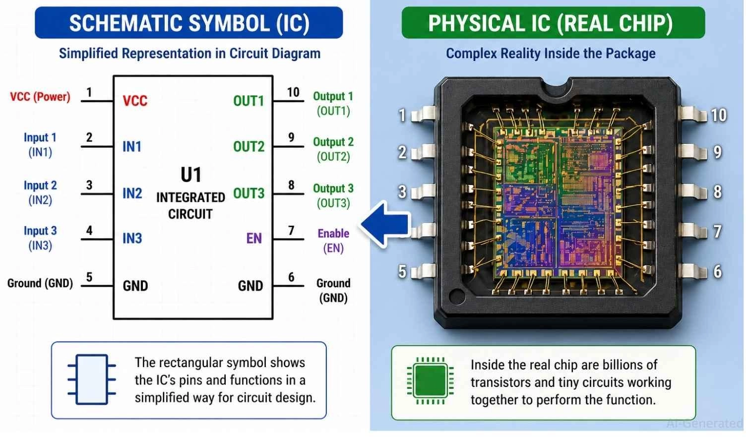
Figure: Demonstrating how a simple rectangular integrated circuit symbol represents complex microscopic circuitry inside a physical chip.
How Integrated Circuit Symbols Work (Pins & Functional Blocks Explained)
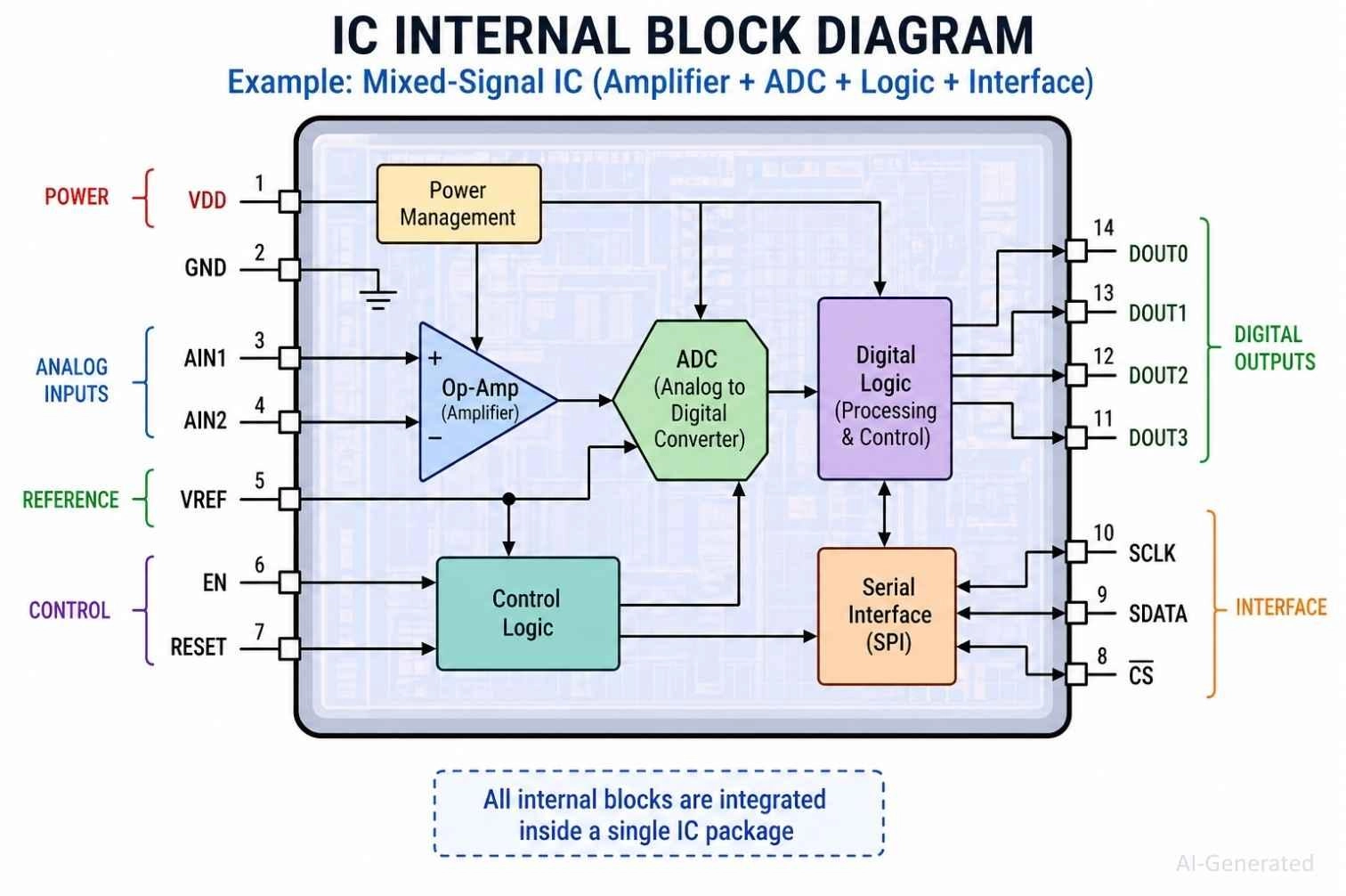
Figure: Internal block diagram of an integrated circuit symbol showing op-amps and ADC blocks inside the main chip boundary.
Why IC Symbols Use Pins Instead of Internal Circuit Details
Drawing billions of internal transistors is impossible. Instead, the symbol uses input, output, and control pins - such as VCC, GND, IN, and OUT - to show exactly how the chip interacts with the outside world.
Internal Functional Blocks in Integrated Circuit Symbols
The symbol represents the internal functional system of the IC, not just its outer shape. The text and labels inside tell you whether it is handling amplifier duties, logic processing, or complex data computing.
Signal Flow Through an Integrated Circuit Symbol Diagram
Understanding an IC symbol pin diagram is all about following the data. Signals enter through input pins, are processed internally, and exit through output pins.
Types of Integrated Circuit Symbols
The most common types of integrated circuit symbols in circuit diagrams include:
- Op-Amp IC: Analog signal amplification
- Logic IC: Digital processing
- Microcontroller IC: System control
- Memory IC: Stores digital data
- Power IC: Voltage regulation and switching
| IC Symbol Type | Symbol Description | Primary Function |
|---|---|---|
| Op-Amp | Triangle shape with (+) and (-) inputs. | Amplifies voltage signals. |
| Logic Gate | Distinct curved or D-shaped symbols (AND, OR, NOT). | Performs digital logic operations. |
| Microcontroller | Large rectangular block with many I/O pins. | Programmable "brain" of the circuit. |
| Voltage Regulator | Simple 3-pin block (IN, GND, OUT). | Provides stable output voltage. |
| Timer IC (555) | Rectangular block with 8 specific function pins. | Generates precise timing pulses. |
| Memory IC | Rectangular block with Address (A0-A7) and Data (D0-D7) lines. | Stores digital information (RAM/ROM). |
Operational Amplifier (Op-Amp) Symbol
Drawn uniquely as a triangle shape, it features non-inverting (+) and inverting (-) inputs, making it perfect for analog signal scaling.
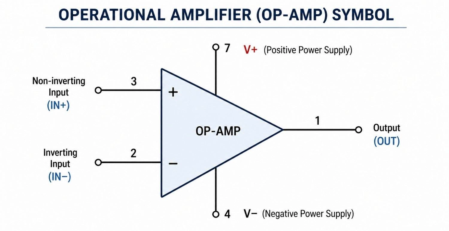
Figure: Schematic symbol of an Operational Amplifier showing input, output, and power pins.
Logic IC Symbols (AND, OR, NOT Gates)
These use specific geometric shapes for digital logic representation, acting as the basic combinational logic for digital computing.
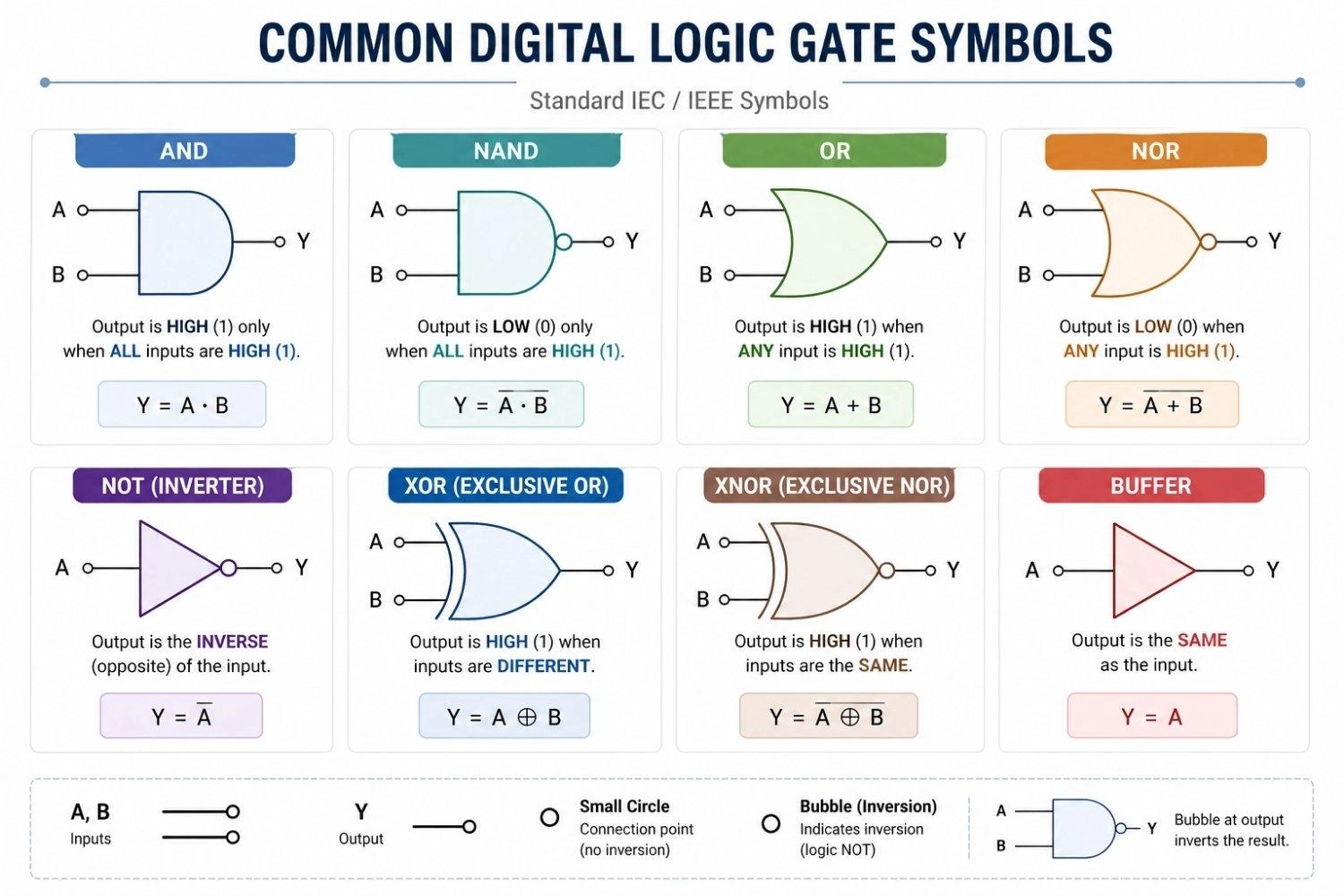
Figure: Individual schematic symbols for digital logic AND, OR, and NOT gates.
Microcontroller Symbol
Drawn as a massive rectangular block featuring multiple I/O pins. To see how complex these get, check out this guide on how to design an ESP32-S2 module PCB.
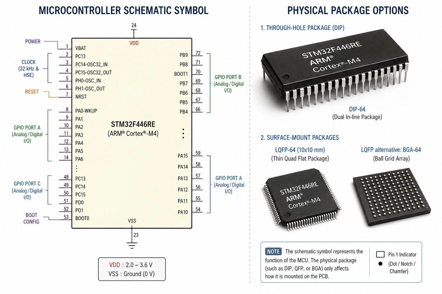
Figure: Microcontroller rectangular schematic symbol alongside its physical DIP and BGA/QFP package equivalents.
Analog Symbols (Amplifier, Comparator)
Often utilizing the same triangle shape as an op-amp, a comparator symbol contrasts two analog voltages and outputs a digital high or low signal.
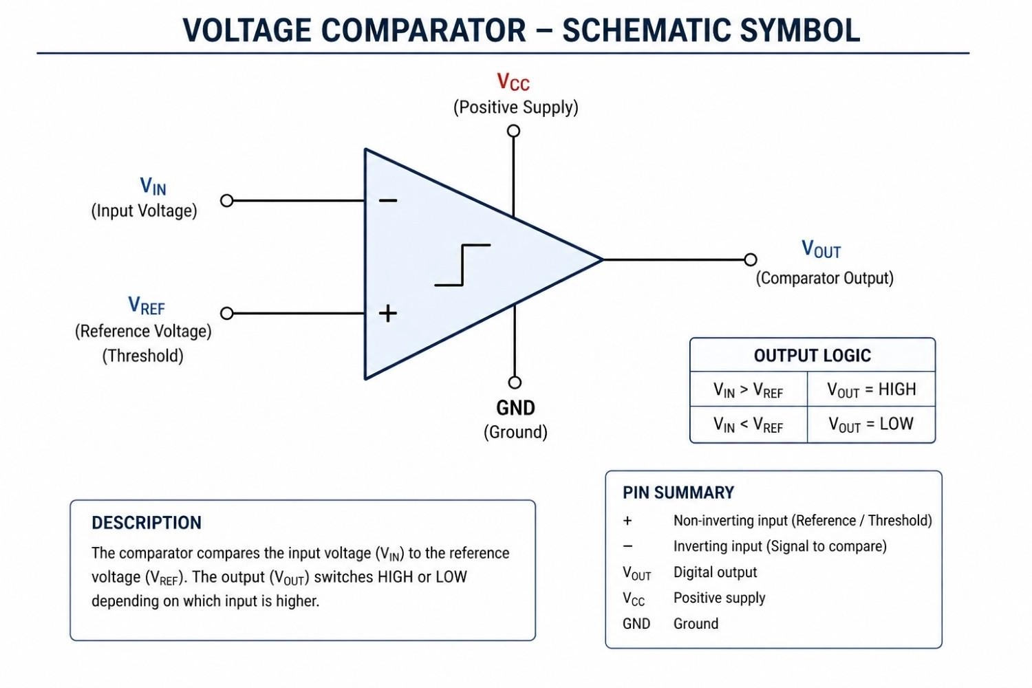
Figure: Schematic symbol of an analog voltage comparator.
Digital IC Symbols (Flip-Flops, Counters)
Used for sequential logic with memory. These symbols feature specific clock input pins (often denoted by a small triangle on the pin line) and standard Q/Q-bar outputs.
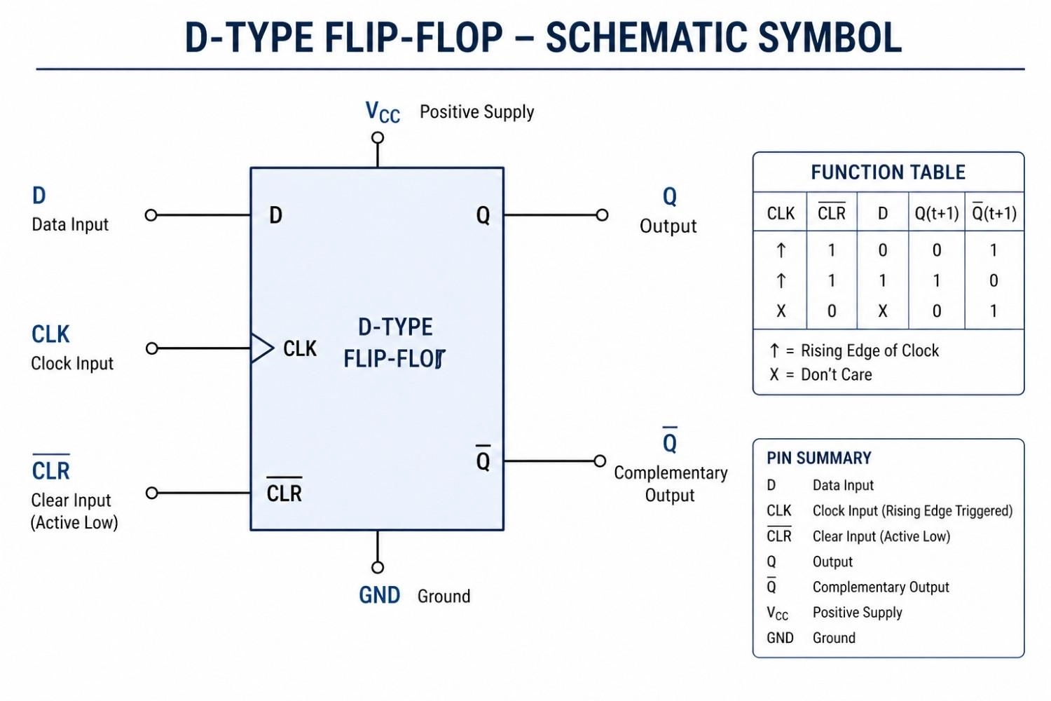
Figure: Digital schematic symbol for a sequential D-Type Flip-Flop.
Memory IC Symbols (RAM, ROM, EEPROM)
Represented as a large rectangular block heavily populated with address lines (A0, A1, etc.) and data lines (D0, D1, etc.) to manage data storage.
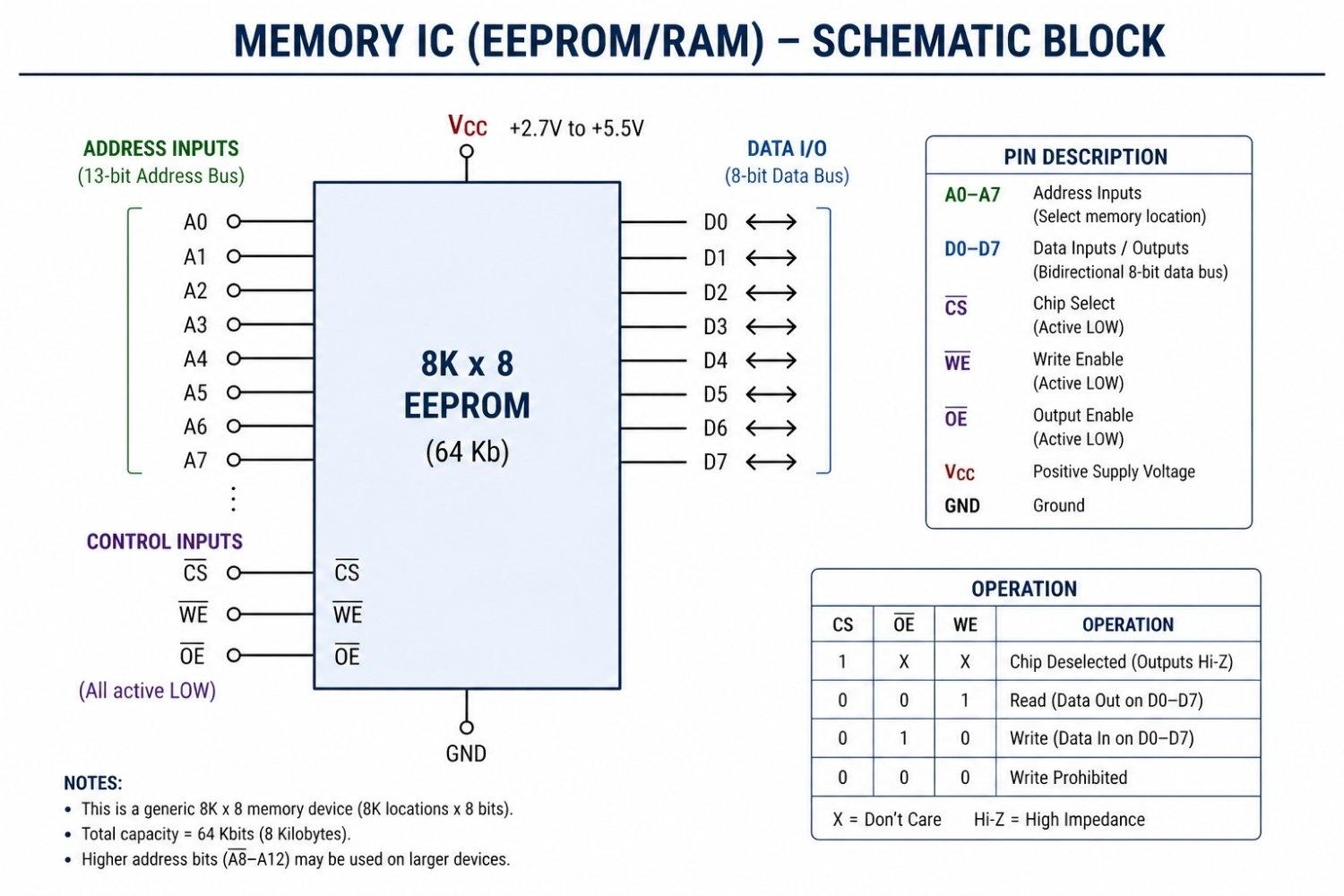
Figure: Schematic block of a Memory IC detailing address lines, data lines, and control pins.
Interface IC Symbols (UART, ADC, DAC)
These utilize a mixed-signal representation. An ADC (Analog-to-Digital Converter) will show analog signal inputs on one side and multiple digital output lines on the other.
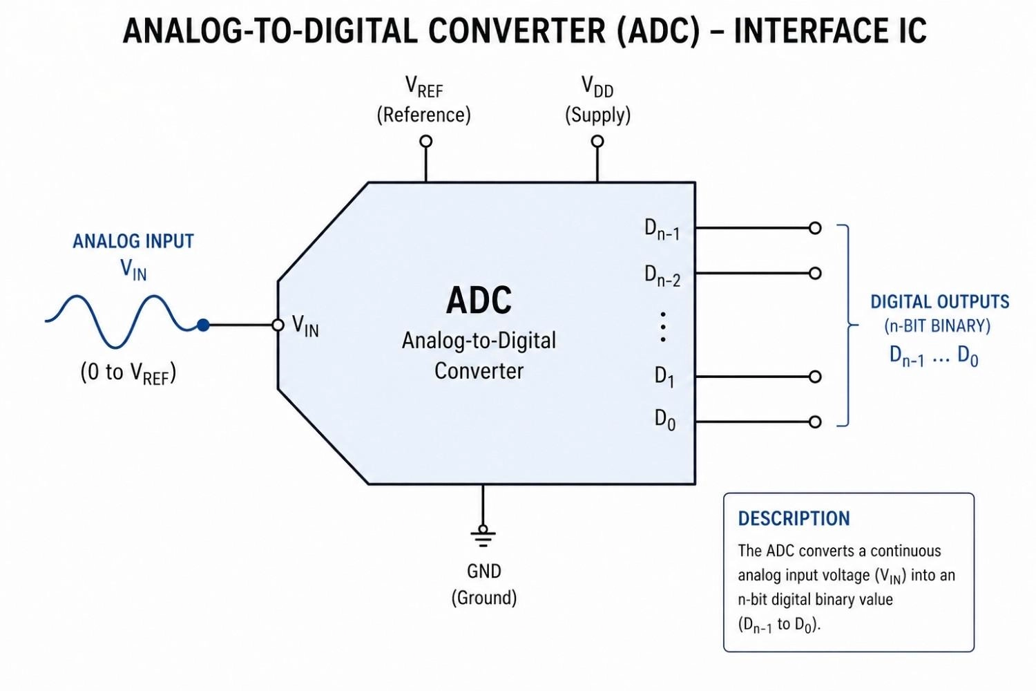
Figure: Schematic symbol of an ADC interface IC converting an analog sigznal into digital outputs.
Power IC Symbols (PMIC, DC-DC Controller)
These switching ICs are critical for battery management. They often feature specialized pins for inductors, feedback loops, and enable signals.
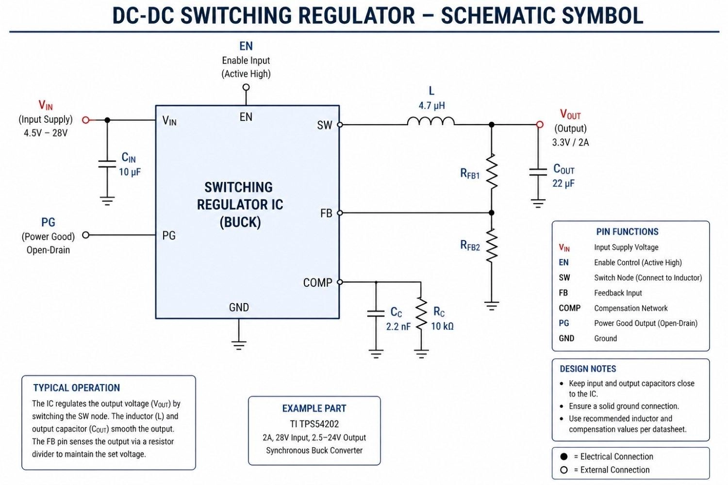
Figure: Schematic symbol of a Power Management IC (PMIC) or DC-DC controller.
How to Read an Integrated Circuit Symbol
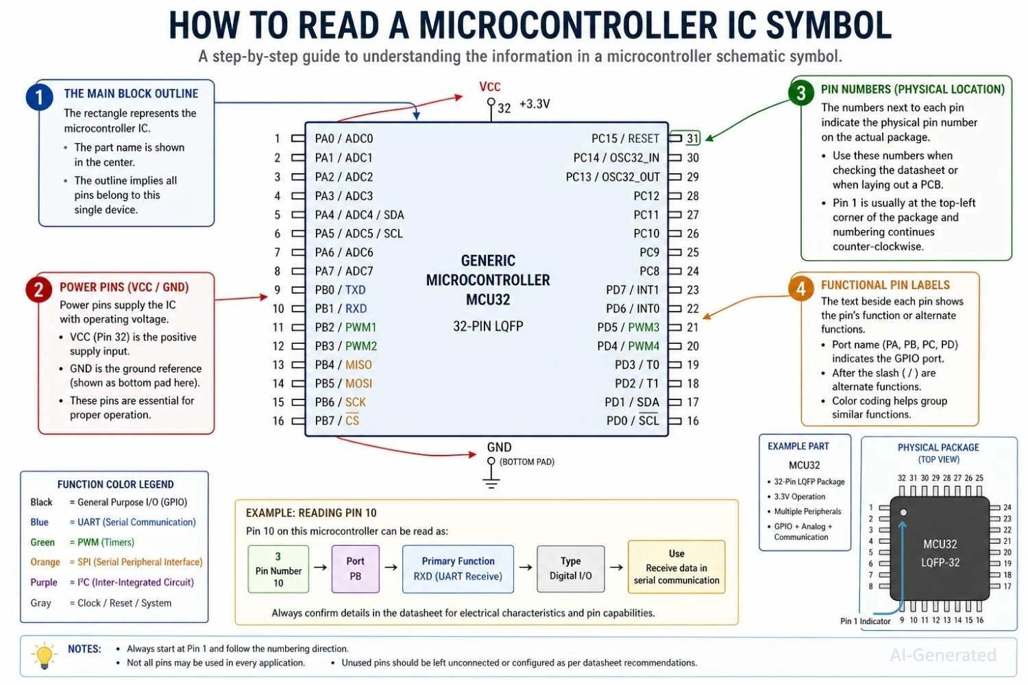
Figure: A step-by-step visual guide on how to read a Microcontroller integrated circuit symbol, highlighting power, pin numbers, and functional labels.
Step 1: Identify IC Block Shape
Start by looking at the overall shape of the symbol. A triangle usually indicates an analog component like an op-amp, while a large rectangular block represents complex digital ICs or microcontrollers.
Step 2: Read Pin Labels
Locate the power and ground pins (VCC, GND) first to establish how the chip is powered. Then, identify the primary inputs (IN) and outputs (OUT) to understand the general signal flow.
Step 3: Check Pin Numbering
Match the small numbers written next to the labels on the schematic with the physical pins on your actual component. This ensures your physical wiring correctly matches the logical design.
Step 4: Analyze Circuit Role
Look at the surrounding components connected to the inputs and outputs. This context helps you deduce the IC's overall purpose, whether it's filtering a signal, switching power, or processing data.
Common Mistakes When Reading IC Symbols
- Ignoring pin labels: Assuming a pin's function based solely on its physical position.
- Confusing functional blocks: Misidentifying a regulator for a transistor due to similar 3-pin symbols.
- Mixing schematic vs physical layout: Trying to wire a breadboard exactly how the rectangular schematic is drawn, rather than following the physical pinout diagram.
Integrated Circuit Package vs. Schematic Symbols (DIP, SMD & Pin Mapping)
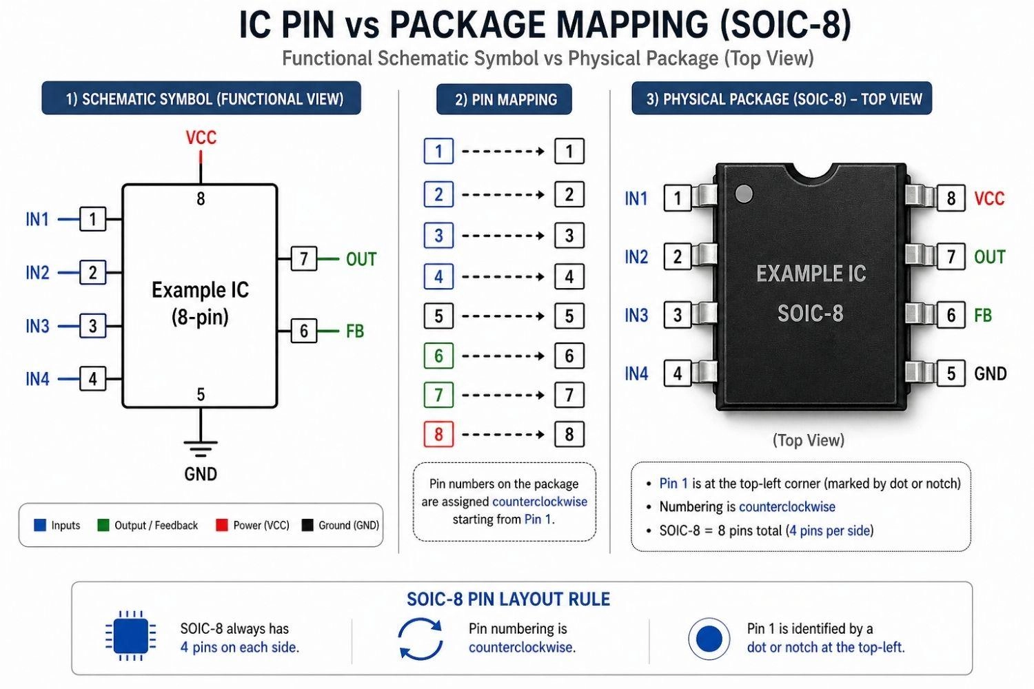
Figure: Comparison showing the difference between a functional IC schematic symbol and a physical IC pin package diagram.
DIP vs SMD IC Symbol Representation
When comparing a DIP vs SMD IC symbol, the schematic block remains the same, but the pin arrangement differs greatly when mapping to the physical PCB footprint. A deep understanding of surface mount vs through-hole packaging is vital here.
Pin Numbering and Labeling in IC Symbols
Pins are numbered sequentially (1, 2, 3...) based on the physical chip, but they are scattered around the schematic symbol based on logic. Always read the labels, not just the numbers.
Functional vs Physical Representation
The biggest hurdle for beginners is understanding the IC pin diagram vs symbol. The schematic symbol shows how it works logically, while the physical pin diagram shows how it is built physically.
Common Integrated Circuit Symbol Examples in Real Circuits
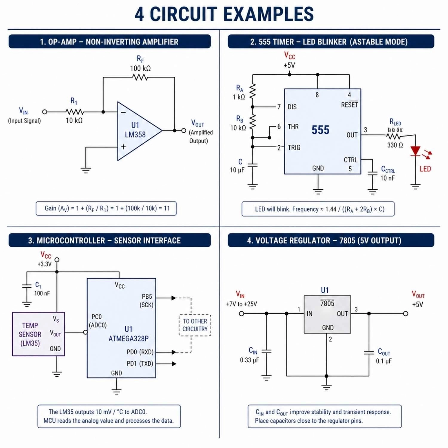
Figure: Four circuit diagram examples showing an Op-Amp, 555 Timer, Microcontroller, and Voltage Regulator in practical use.
Op-Amp Circuit Example
- Used for amplification of weak audio or sensor signals.
- Wired with feedback resistors to set the exact gain.
555 Timer Circuit
- Used for precise pulse generation.
- Easily wired to create flashing LEDs or clock signals.
Microcontroller Circuit
- Acts as the main control system for smart devices.
- Interfaces with sensors, motors, and displays simultaneously.
Voltage Regulator Circuit
- Ensures a completely stable voltage for delicate processors.
- Placed immediately after a power supply with bypass capacitors.
Integrated Circuit Symbol vs Other Electronic Symbols
IC Symbol vs Op-Amp Symbol
- Op-Amp = A specific type of analog IC with a dedicated triangle symbol.
- IC = The general rectangular block used to represent a wide range of IC devices.
IC Symbol vs Transistor Symbol
- IC = Integrates multiple devices into one block.
- Transistor = A single, discrete semiconductor device.
IC Symbol vs Resistor Symbol
- IC = An active component that manipulates signals and requires power.
- Resistor = A passive component that simply resists current flow.
IC vs Discrete Components
While discrete components do one specific job, an IC integrates multiple functions, replacing dozens or hundreds of discrete parts on a board.
From Integrated Circuit Symbol to PCB Design and Assembly
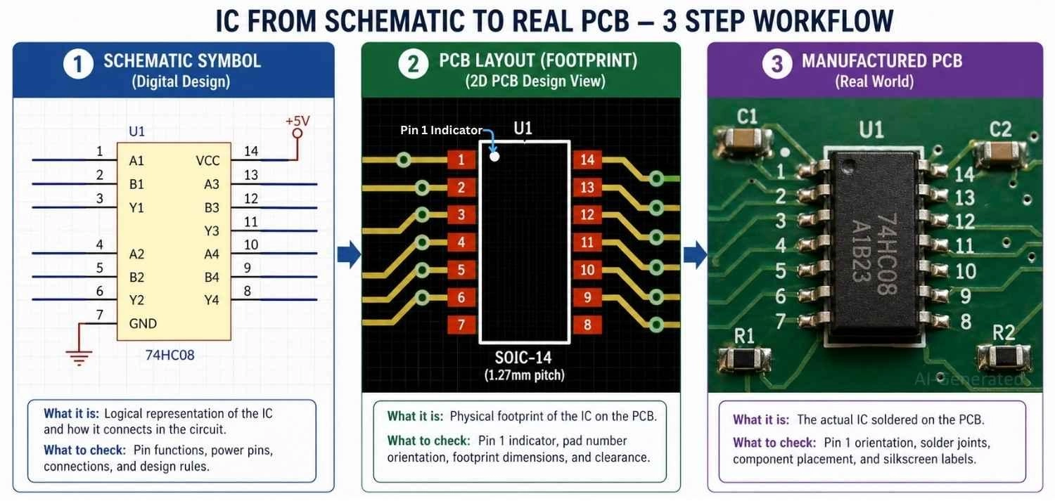
Figure: Visual workflow showing an integrated circuit transitioning from a digital schematic symbol, to a PCB footprint layout, and finally to a physical component soldered on a manufactured board.
Integrated Circuit Symbol to PCB Workflow
Convert IC Symbol to Footprint (Logical → Physical Mapping): Transitioning from schematic to PCB is not just a visual step - it is a data integrity process.
- The schematic symbol defines logical connectivity (netlist)
- The footprint defines physical geometry (pads, pitch, orientation)
These two must be linked via a component library entry.
Key Technical Points:
- Ensure pin count matches exactly (no hidden pins mismatch)
- Handle multi-unit symbols (e.g., op-amps split into A/B units)
- Assign correct electrical pin types (input, output, power, passive)
Assigning Footprints for Integrated Circuit Symbols
- Match package (DIP, QFN, SOIC) to your specific component by double-checking the exact dimensions in the manufacturer's datasheet.
- Verify pin 1 orientation, which is usually marked by a small dot, notch, or line on both the footprint silkscreen and the physical chip.
Incorrect pin mapping in IC design is a common cause of PCB failure.
Use JLCPCB Parts Library to quickly verify the correct symbol-footprint pairing and avoid pin-mapping errors before layout.
IC PCB Assembly (PCBA) with JLCPCB
Transitioning from schematic to hardware requires precise symbol-to-footprint mapping, pin alignment, and package verification - especially for dense ICs and SMD devices.
A professional PCB assembly service like JLCPCB helps eliminate common risks such as pin mismatches, orientation errors, and soldering defects, ensuring your design is manufactured exactly as intended.
FAQs About Integrated Circuit Symbol
Q: What does an integrated circuit symbol represent?
It represents a complete electronic system integrated into a single component.
Q: Why are IC symbols rectangular?
The rectangular block provides a clean, standard way to organize and label numerous input and output pins.
Q: How to identify IC pins in a schematic?
Look for the text labels (like IN, OUT, VCC) inside the block, and the physical pin numbers written just outside the block.
Q: What is the difference between IC symbol and pin diagram?
The symbol shows logical function in a schematic, while the pin diagram shows the physical layout of the real chip.
Q: Are IC symbols standardized?
Yes, most follow IEEE/ANSI standards, though complex microcontrollers are custom-drawn by engineers based on specific needs.
Conclusion
The integrated circuit symbol is the ultimate tool for simplifying complex electronics. By understanding IC symbols, you can quickly interpret how complex systems process signals, manage logic, and control power in real circuits. They are absolutely essential for moving from theoretical breadboard sketches to professional PCB design.
Popular Articles
• How to Identify SMD LED Polarity: Markings, Testing, and PCB Tips
• How to Create a Bluetooth-Controlled Car With Arduino: A Step-by-Step Guide
• How to Design and Assemble a Reliable ESP32 Module PCB on a 2-Layer Board
• The Ultimate Guide to Relay Symbol: Coil, Contacts, Diagrams, and Circuit Applications
• The Ultimate Guide to PCBA: Process,Types and Techniques for the Electronics Enthusiast
Keep Learning
How to Design an ESP32-S3 Development Board from Scratch: A 4-Layer PCB Design Tutorial
Designing your own ESP32-S3 development board gives you complete control over your hardware architecture while preparing your IoT projects for commercial production. Instead of relying on bulkier, off-the-shelf boards, building a custom design allows you to optimize the board space, expose only the required GPIO pins, and integrate peripherals directly onto a single substrate. In this tutorial, we will design a 4-layer ESP32-S3 development board from scratch. We will walk through the entire hardware d......
Circuit Breaker Symbols Explained: IEC, ANSI, MCB, and Pole Configuration Symbols
Electrical schematics are the universal language of power systems, control circuits, and printed circuit boards. Within these diagrams, the circuit breaker symbol is one of the most critical elements. Getting it right is essential for safety, troubleshooting, and manufacturing. An error as simple as mixing up a circuit breaker with a manual switch or an isolator can lead to catastrophic misinterpretations on the factory floor or during field maintenance. This guide provides a complete, technically acc......
How to Identify SMD LED Polarity: Markings, Testing, and PCB Tips
Surface-mount LED components are ubiquitous in electronics design, serving as everything from simple power indicators to complex lighting arrays. Unlike standard resistors, LEDs are polarized diodes. Identifying SMD LED polarity correctly is critical for prototype troubleshooting and high-volume PCB assembly. A reversed LED results in no light output, broken circuit paths, and potential diode breakdown if the reverse voltage exceeds the component's maximum rating (typically 5V or less for most indicat......
Arduino LED Driver Tutorial: Control More LEDs with 74HC595 and MAX7219
Arduino GPIO pins run out quickly in larger LED projects. By utilizing dedicated LED drivers and expansion ICs, you can drastically reduce pin usage, eliminate processor-heavy multiplexing loops, and simplify display wiring. In this guide, you will learn the operational architecture, wiring configurations, cascading techniques, and optimization strategies for the 74HC595 shift register and the MAX7219 LED driver. Why Arduino Projects Need LED Driver ICs Arduino GPIO and Current Limitations An ATmega32......
How to Create a Bluetooth-Controlled Car With Arduino: A Step-by-Step Guide
This tutorial walks through the complete engineering and implementation of a two-wheel Bluetooth RC car with an Arduino Nano module on a specially designed PCBA (Printed Circuit Board Assembly). While many hobbyists start by wiring motors and Bluetooth modules with jumper cables on a breadboard, this approach is prone to disconnection and signal noise. This guide upgrades that process by teaching you how to design a professional mainboard. Key Design Features Controller: Arduino Nano used as a plug-in......
Fiducial Marks in PCB and SMT Assembly: A Complete Guide to Accuracy and Design Rules
Modern Printed Circuit Boards (PCBs) are complex, integrating high-density components like 0.4mm pitch Ball Grid Arrays (BGAs), 0201 passives, and fine-pitch Quad Flat No-Lead (QFN) packages. In this advanced manufacturing environment, achieving placement accuracy measured in micrometers is crucial. A significant challenge in automated manufacturing is how pick-and-place machines, which handle thousands of components per hour, precisely locate the PCB. A board on a conveyor system is never in the perf......